

Page 1
®
HIGH VOLTAGE FAST-SWITCHING
■ HIGH VOLTAGE CAPABILITY
■ MINIMUM LOT- TO- LO T SPR E AD FO R
RELIABLE OPERATION
■ LOW BASE-DRIVE REQUIREMENTS
■ VERY H IGH SWI TCHING SPEED
■ FULLY CHARACTERIZED AT 125
APPLICATIONS
■ ELECTRONIC TRANSFORMER FOR
HALOGEN LAM PS
■ SWITCH MODE P OW ER SUP P LIE S
o
C
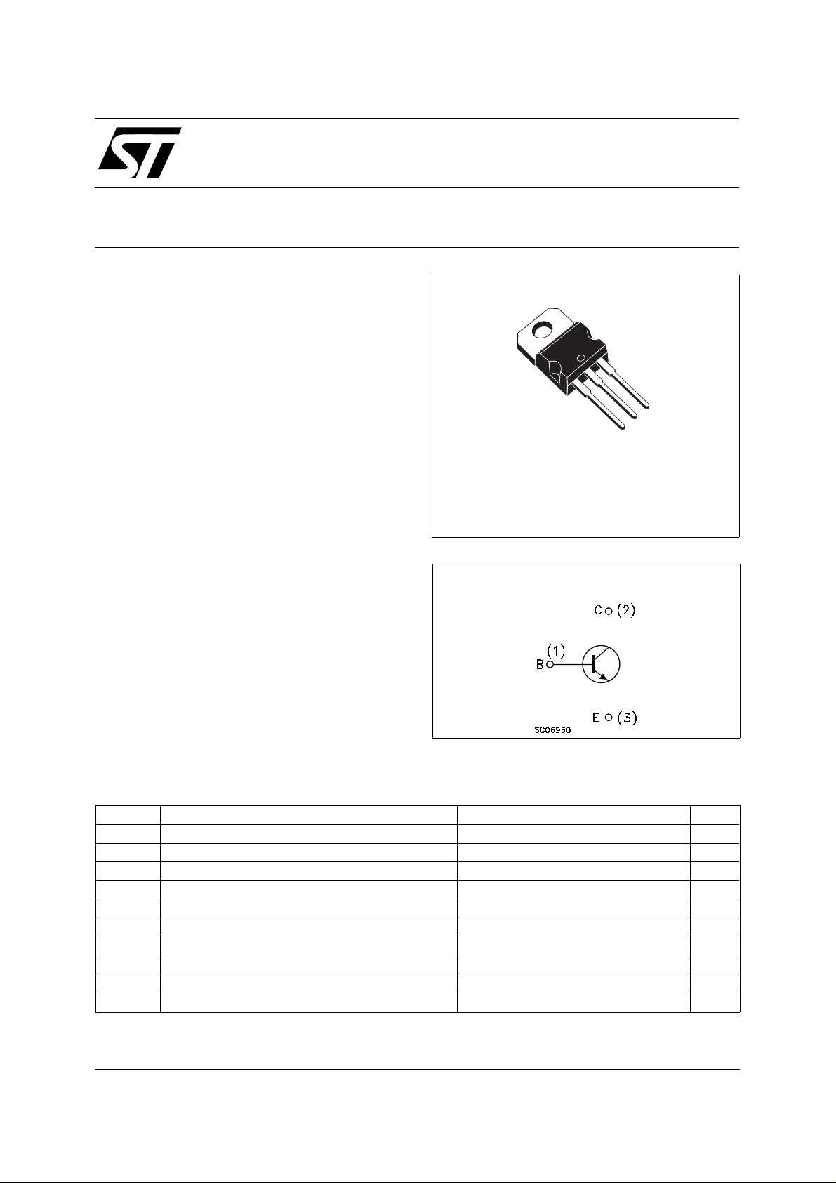
BUL654
NPN POW ER TRANSISTOR
PRELIMINARY DATA
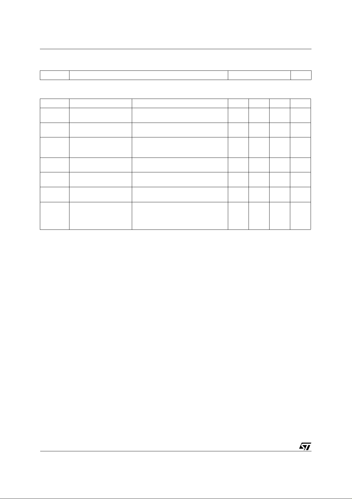
3
2
1
DESCRIPTION
TO-220
The BUL654 is manufactured using high voltage
Multi Epitaxial Planar technology for cost-effectiv e
high performance. It uses a Hollow Emitter
structure to enhance switchi ng speeds.
The BUL series is designed for use in lighting
applications and low cost switch-mode power
INTERNAL SCHEMATIC DIAGRAM
supplies.
ABSOL UT E MAXIMU M RATINGS
Symbol Parameter Value Unit
V
V
V
I
I
P
T
Collector-Emitter Voltage (VBE = 0) 700 V
CES
Collector-Emitter Voltage (IB = 0) 400 V
CEO
Emitter-Base Voltage (IC = 0) 9 V
EBO
Collector Current 12 A
I
C
Collector Peak Current (tp < 5 ms) 18 A
CM
Base Current 6 A
I
B
Base Peak Current (tp < 5 ms) 9 A
BM
Total Dissipation at Tc = 25 oC80W
tot
Storage Temperature -65 to 150
stg
Max. Operating Junction Temperature 150
T
j
o
C
o
C
February 2003
1/4
Page 2
BUL654
THERMAL DATA
R
thj-case
Thermal Resistance Junction-Case Max 1.25
o
C/W
ELECTRICAL CHARACTERISTICS (T
= 25 oC unless otherwise specified)
case
Symbol Parameter Test Conditions Min. Typ. Max. Unit
I
CES
I
CEO
V
CEO(sus)
Collector Cut-off
Current (V
BE
= 0)
Collector Cut-off
Current (I
= 0)
B
∗ Collector-Emitter
= 700 V
V
CE
V
= 700 V Tc = 125 oC
CE
= 400 V 100 µA
V
CE
= 100 mA L = 25 mH 400 V
I
C
50
500
Sustaining Voltage
(I
= 0)
B
V
V
CE(sat)
EBO
Emitter-Base Voltage
(I
= 0)
C
∗ Collector-Emitter
Saturation Voltage
V
∗ Base-Emitter
BE(sat)
Saturation Voltage
h
∗ DC Current Gain IC = 10 mA VCE = 2 V
FE
∗ Pulsed: Pulse duration = 300 µs, duty cycle 1.5 %
= 10 mA 9 V
I
E
IC = 2 A IB = 0.4 A
I
= 7 A IB = 1.4 A
C
IC = 2 A IB = 0.4 A
I
= 7 A IB = 1.4 A
C
0.15
0.35
0.85
1
0.3
0.7
1
1.2
15
I
= 2 A VCE = 2 V
C
I
= 6 A VCE = 2 V
C
I
= 12 A VCE = 5 V
C
15
7
4
µA
µA
V
V
V
V
2/4
Page 3

TO-220 MECHANICAL DATA
BUL654
DIM.
A 4.40 4.60 0.173 0.181
C 1.23 1.32 0.048 0.052
D 2.40 2.72 0.094 0.107
E 0.49 0.70 0.019 0.027
F 0.61 0.88 0.024 0.034
F1 1.14 1.70 0.044 0.067
F2 1.14 1.70 0.044 0.067
G 4.95 5.15 0.194 0.202
G1 2.40 2.70 0.094 0.106
H2 10.00 10.40 0.394 0.409
L2 16.40 0.645
L4 13.00 14.00 0.511 0.551
L5 2.65 2.95 0.104 0.116
L6 15.25 15.75 0.600 0.620
L7 6.20 6.60 0.244 0.260
L9 3.50 3.93 0.137 0.154
M 2.60 0.102
DIA. 3.75 3.85 0.147 0.151
MIN. TYP. MAX. MIN. TYP. MAX.
mm inch
P011CI
3/4
Page 4

BUL654
Information furnished is believed to be accurate and reliable. However, STMicroelectronics assumes no responsibility for the consequences
of use of such inform ation nor for any infringe ment o f patents or other rig hts o f third par ties which ma y resul t from i ts use. N o li cen se is
granted by implicatio n or otherwise under any patent or patent rights of STMicroelectronics. Specification mentioned in this publication are
subject to change without notice. This publication supersedes and replaces all information previously supplied. STMicroelectronics products
are not authorized for use as critical compo nents in life support devices or systems without express written approval of STMicroelectronics.
The ST logo is a trademark of STMicroelectronics
© 2003 STMicroelectro nics – Printed in Italy – All Rights Reserved
STMicroelectronics GROUP OF COMPANIES
Australia - Brazil - Canada - China - Finland - France - Germany - Hong Kong - India - Israel - Italy - Japan - Malaysia - Malta - Morocco -
Singapore - Spain - Sweden - Switzerland - United Kingdom - United States.
http://www.st.com
4/4
 Loading...