

Page 1
HIGH VOLTAGE FAST-SWITCHING
■ STMicroelectronics PREFERRED
SALESTYPE
■ HIGH VOLTAGECAPABILITY
■ LOW SPREAD OF DYNAMICPARAMETERS
■ MINIMUMLOT-TO-LOT SPREAD FOR
RELIABLEOPERATION
■ LOW BASE-DRIVEREQUIREMENTS
■ VERYHIGH SWITCHINGSPEED
■ FULLYCHARACTERISED AT 125
■ HIGH RUGGEDNESS
■ INTEGRATED ANTIPARALLEL
COLLECTOR-EMITTERDIODE
APPLICATIONS
■ ELECTRONICTRANSFORMERS FOR
HALOGENLAMPS
■ SWITCHMODEPOWER SUPPLIES
o
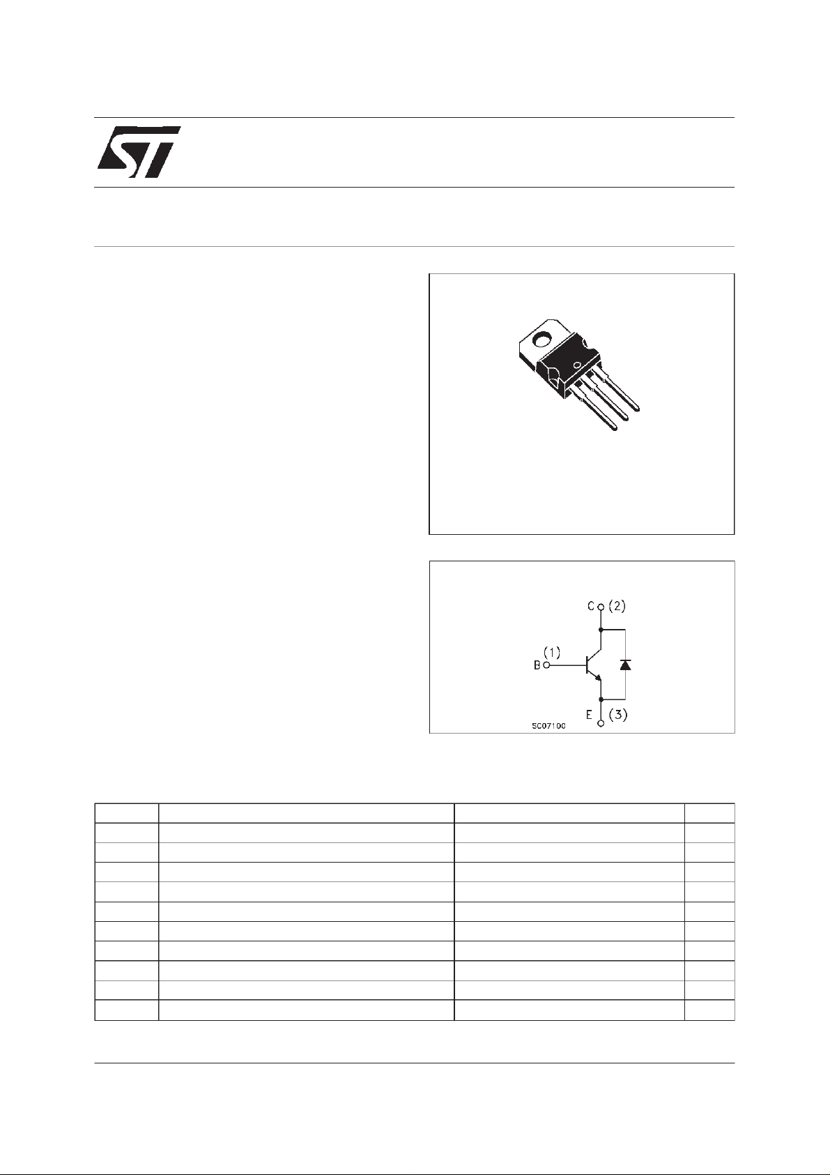
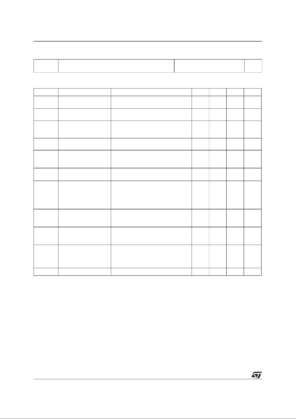
C
BUL38D
NPN POWER TRANSISTOR
3
2
1
TO-220
DESCRIPTION
INTERNAL SCHEMATIC DIAGRAM
The BUL38D is manufacturedusing high voltage
Multi Epitaxial Planar technology for high
switching speeds and high voltage withstand
capability.
The BUL series is designed for use in lighting
applications and low cost switch-mode power
supplies.
ABSOLUTE MAXIMUM RATINGS
Symb o l Para meter Val u e Uni t
V
V
V
I
I
P
T
Collector-Emitter Voltage (VBE= 0 ) 800 V
CES
Collector-Emitter Voltage (IB= 0 ) 450 V
CEO
Emitter-Base Voltage (IC=0) 9 V
EBO
I
Collector Current 5 V
C
Collector Peak Current (tp<5 ms) 1 0 A
CM
I
Base Current 2 A
B
Base Peak Curre nt (tp<5 ms) 4 A
BM
Tot al Diss ip at i on at Tc = 25oC80W
tot
Sto rage T emperat ure -65 to 150
stg
Max. Oper at in g Junct ion Te mperatu re 150
T
j
o
C
o
C
June 2000
1/6
Page 2
BUL38D
THERMAL DATA
R
thj-case
R
thj-amb
Ther mal Resistan ce Junct ion-Case Max
Ther mal Resistan ce Junct ion-Am bie nt Max
1.56
62.5
o
C/W
o
C/W
ELECTRICAL CHARACTERISTICS (T
=25oC unlessotherwise specified)
case
Symbol Parameter Test Cond ition s Min. Typ. Max. Un it
I
CES
I
CEO
V
CEO(sus)
Collec t or Cut -off
Current (V
BE
=0)
Collec t or Cut -off
Current (I
B
=0)
∗ Collec tor -Emit t er
V
=800V
CE
=800V Tj=125oC
V
CE
V
= 450 V 250 µA
CE
I
= 10 0 mA L = 25 mH 450 V
C
100
500
Sust aining Voltage
=0)
(I
B
V
EBO
V
CE(sat)
V
BE(sat)
h
FE
t
t
t
V
∗
Pulsed: Pulse duration = 300 µs, duty cycle1.5 %.
The product is pre-selected in DC current gain (Group A and Group B). STMicroelectronics reserves the right to ship either groups
according to production availability. Please contact your nearest STMicrolectronics salesoffice for deliverydatails.
Emitter-Base Voltage
(I
=0)
C
∗ Collector-Emit t er
Saturation Voltage
∗ Base-Emitt er
Saturation Voltage
∗ DC Current Ga in IC=10mA VCE=5V
RESI STIVE LOAD
Storage Time
s
t
Fall Time
f
INDUCTIVE LO AD
Storage Time
s
t
Fall Time
f
INDUCTIVE LO AD
Storage Time
s
t
Fall Time
f
Diode Forward V oltage IC=2A 1.5 V
f
=10mA 9 V
I
E
IC=1A IB=0.2A
=2A IB=0.4A
I
C
=3A IB=0.75A
I
C
IC=1A IB=0.2A
=2A IB=0.4A
I
C
10
=0.5A VCE=5V
I
C
=2A VCE=5V
I
C
Gr oup A
Gr oup B
13
22
IC=2.5A VCC=150V
=-IB2=0.5A tp=30µs
I
B1
1.0 2.2
IC=2A IB1=0.4A
V
V
=-5V RBB=0Ω
BE(off)
= 2 50 V L = 200 µH
CL
1
55
IC=2A IB1=0.4A
V
V
T
=-5V RBB=0Ω
BE(off)
= 2 50 V L = 200 µH
CL
=125oC
j
1.3
100
0.5
0.7
1.1
1.1
1.2
60
23
32
0.8
1.8
100
µA
µA
V
V
V
V
V
µs
µs
µs
ns
µs
ns
2/6
Page 3

BUL38D
Safe OperatingArea
DCCurrent Gain
DeratingCurve
DC Current Gain
Collector-Emitter SaturationVoltage
Base-EmitterSaturation Voltage
3/6
Page 4

BUL38D
InductiveStorage Time
ReverseBiased SOA
InductiveFall Time
RBSOAand InductiveLoad SwitchingTest
Circuit
4/6
(1) Fast electronic switch
(2)Non-inductive Resistor
(3) Fast recovery rectifier
Page 5

TO-220 MECHANICAL DATA
BUL38D
DIM.
MIN. TYP. MAX. MIN. TYP. MAX.
A 4.40 4.60 0.173 0.181
C 1.23 1.32 0.048 0.051
D 2.40 2.72 0.094 0.107
D1 1.27 0.050
E 0.49 0.70 0.019 0.027
F 0.61 0.88 0.024 0.034
F1 1.14 1.70 0.044 0.067
F2 1.14 1.70 0.044 0.067
G 4.95 5.15 0.194 0.203
G1 2.4 2.7 0.094 0.106
H2 10.0 10.40 0.393 0.409
L2 16.4 0.645
L4 13.0 14.0 0.511 0.551
L5 2.65 2.95 0.104 0.116
L6 15.25 15.75 0.600 0.620
L7 6.2 6.6 0.244 0.260
L9 3.5 3.93 0.137 0.154
DIA. 3.75 3.85 0.147 0.151
mm inch
P011C
5/6
Page 6

BUL38D
Information furnished isbelieved tobe accurate and reliable. However, STMicroelectronics assumes no responsibility for theconsequences
of use of such information nor for any infringement of patents or other rights of third parties which may result from its use. No license is
granted by implication or otherwise under any patent or patent rights of STMicroelectronics. Specification mentioned in this publication are
subject tochange without notice. This publication supersedes and replaces all information previously supplied. STMicroelectronics products
are not authorized for use as critical components in life support devices or systems without express written approval of STMicroelectronics.
The ST logo is a trademark of STMicroelectronics
2000 STMicroelectronics – Printed in Italy – All Rights Reserved
STMicroelectronicsGROUP OF COMPANIES
Australia - Brazil - China - Finland - France - Germany - Hong Kong - India- Italy- Japan - Malaysia - Malta - Morocco -
Singapore- Spain - Sweden - Switzerland -United Kingdom - U.S.A.
http://www.st.com
6/6
 Loading...