

Page 1
®
HIGH VOLTAGE FAS T-SWITCHING
■ INTEGRATED ANTISATURATION AND
PROTECTION NETWORK
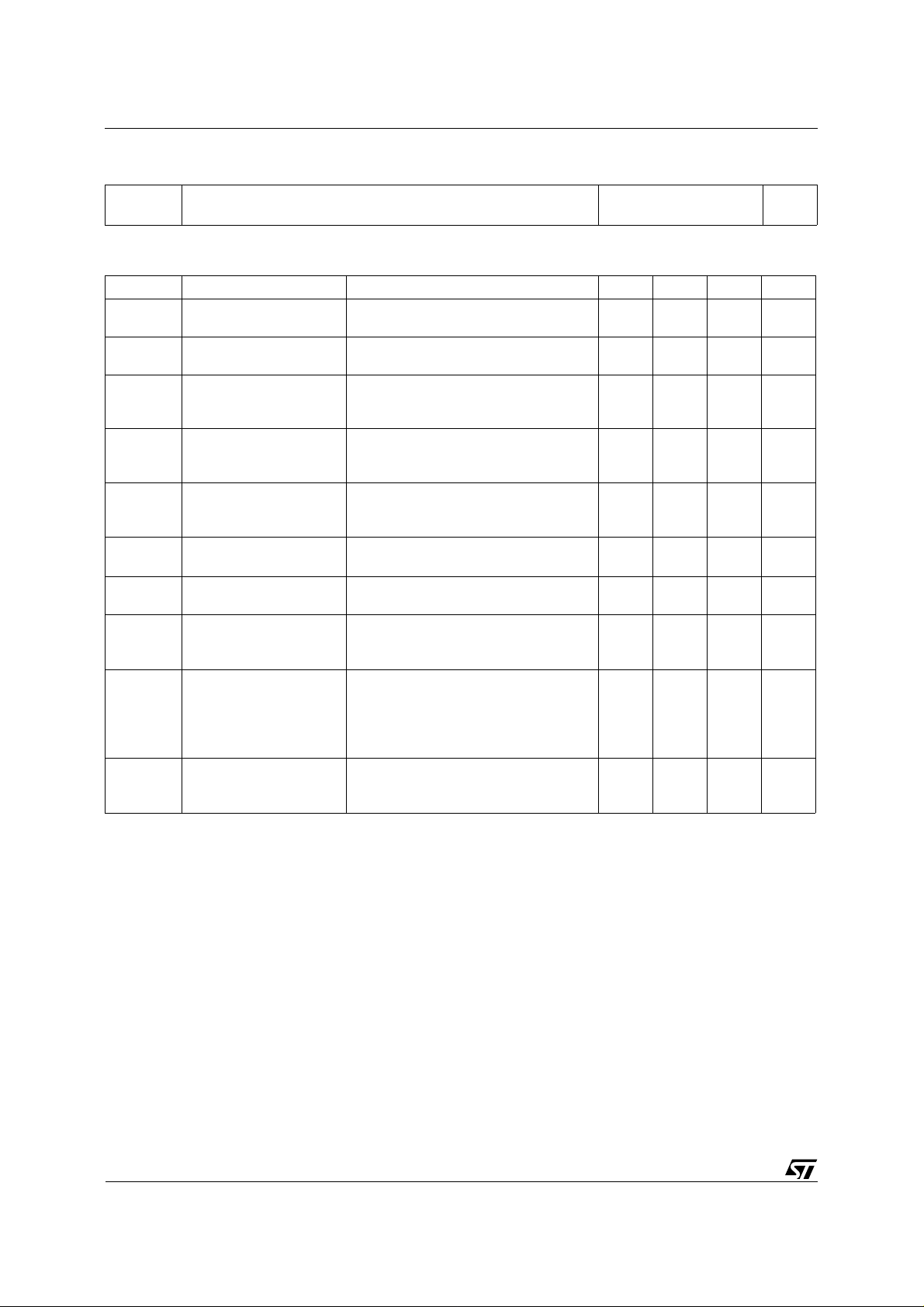
■ INTEGRATED ANTIPARALLEL COLLECTOR
EMITTER DIODE
■ HIGH VOLTAGE CAPABILITY
■ LOW SPREAD OF DYNA MIC PA RA ME TERS
■ MINIMUM LOT-TO-LOT SPRE AD F O R
RELIABLE OPERATION
■ VERY H IGH SWITCHING SPE ED
■ ARCING TEST SELF PROTECTED
BUL1603ED
NPN POW ER TRANSISTOR
PRELIMINARY DATA
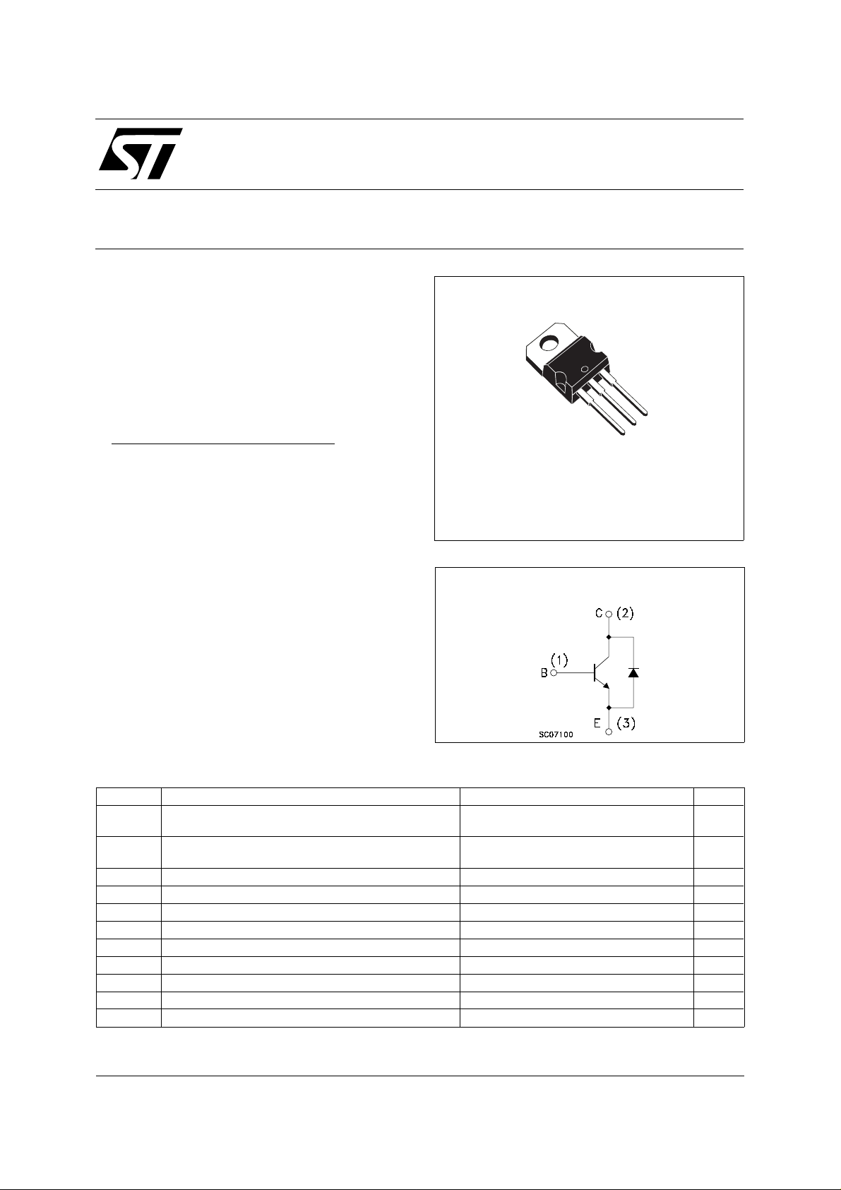
3
2
1
APPLICATIONS
■ TWO LAMPS ELECTRONIC BALLAST FOR
FLUORESCENT LIGHTING 277 V
AC
IN
TO-220
PUSH-PULL CONF IGURA TION
DESCRIPTION
The BUL1603ED is a new device designed for
fluorescent electronic ballast 277 V
push-pull
AC
INTER NAL SCH E M ATI C DIAG RA M
applications.
This device can be used without baker clamp and
transil protection, reducing greatly the component
count.
ABSOLUTE MAXIMUM RATINGS
Symbol Parameter Value Unit
V
V
V
V
I
I
P
T
Collector-Emitter Voltage
CES
(V
= 0; I
BE
Collector-Emitter Voltage
CES
(VBE = 0; I
Collector-Emitter Voltage (IB = 0) 650 V
CEO
Emitter-Base Voltage (IC = 0) 11 V
EBO
I
Collector Current 3 A
C
Collector Peak Current (tp <5 ms) 6 A
CM
I
Base Current 2 A
B
Base Peak Current (tp <5 ms) 4 A
BM
Total Dissipation at Tc = 25 oC80W
tot
Storage Temperature -65 to 150
stg
T
Max. Operating Junction Temperature 150
j
= 10 mA; )
CES
= 100 µA; )
CES
1600 V
1550 V
o
C
o
C
September 2002
1/6
Page 2
BUL1603ED
THERMAL DATA
R
thj-case
R
thj-amb
Thermal Resistance Junction-Case Max
Thermal Resistance Junction-Ambient Max
1.56
62.5
o
C/W
o
C/W
ELECTRICAL CHARACTERISTICS (T
= 25 oC unless otherwise specified)
case
Symbol Parameter Test Conditions Min. Typ. Max. Unit
I
CES
I
EBO
V
(BR)CES
V
CEO(sus)
Collector Cut-off
Current (V
BE
= 0)
Emitter Cut-off Current
(I
= 0)
C
Collector-Emitter
Breakdown Voltage
(V
= 0)
BE
∗ Collector-Emitter
= 1550 V 100 µA
V
CE
= 9 V 100 µA
V
EB
I
= 10 mA
C
= 100 µA
I
C
I
= 100 mA L = 25 mH 650 V
C
1600
1550
Sustaining Voltage
(I
= 0)
B
V
(BR)EBO
Emitter-Base
I
= 10 mA 11 18 V
E
Breakdown Voltage
(I
= 0)
C
∗ Collector-Emitter
V
CE(sat)
Saturation Voltage
V
∗ Base-Emitter
BE(sat)
IC = 1 A IB = 0.25 A
I
= 0.25 A IB = 0.025 A
C
1.5
1.5
IC = 1 A IB = 0.25 A 1.2 V
Saturation Voltage
h
∗ DC Current Gain IC = 5 mA VCE = 10 V
FE
I
= 0.4 A VCE = 3 V
C
I
= 1 A VCE = 1.5 V
C
18
15
4
40
RESISTIVE LOAD
t
t
E
Delay Time
d
Rise Time
t
r
Storage Time
s
Fall Time
t
f
Repetitive Avalanche
ar
Energy
I
= 0.5 A VCC = 125 V
C
I
= 0.05 A IB2 = -0.25 A
B1
D.C. = 2% P.W. = 300 µs
(see figure 1)
L = 2 mH C = 1.8 nF
V
= 50 V VBE = -5 V
CC
0.3
0.8
1.2
0.35
6mJ
(see figure 2)
∗ Pulsed: Pulse duration = 300 µs, duty cycle 1.5 %
V
V
V
V
µs
µs
µs
µs
2/6
Page 3

BUL1603ED
Safe Operating Are a
Output Characteris tics
Derating Curve
DC Current Gain
DC Current Gain
Collector Emitter Sat urat i on Voltag e
3/6
Page 4

BUL1603ED
Base Emitter Sat urat ion Voltage
Figure 1: Resistive Load S witching Test Circuit
1) Fast electronic switch
2) Non-inductive Resistor
Figure 2: Energy Rating Test Circuit
4/6
Page 5

TO-220 MECHANICAL DATA
BUL1603ED
DIM.
A 4.40 4.60 0.173 0.181
C 1.23 1.32 0.048 0.052
D 2.40 2.72 0.094 0.107
E 0.49 0.70 0.019 0.027
F 0.61 0.88 0.024 0.034
F1 1.14 1.70 0.044 0.067
F2 1.14 1.70 0.044 0.067
G 4.95 5.15 0.194 0.202
G1 2.40 2.70 0.094 0.106
H2 10.00 10.40 0.394 0.409
L2 16.40 0.645
L4 13.00 14.00 0.511 0.551
L5 2.65 2.95 0.104 0.116
L6 15.25 15.75 0.600 0.620
L7 6.20 6.60 0.244 0.260
L9 3.50 3.93 0.137 0.154
M 2.60 0.102
DIA. 3.75 3.85 0.147 0.151
MIN. TYP. MAX. MIN. TYP. MAX.
mm inch
P011CI
5/6
Page 6

BUL1603ED
Information furnished is believed to be accurate and reliable. However, STMicroelectronics assumes no responsibility for the consequences
of use of such inform ation nor for any infringe ment o f patents or other rig hts o f third par ties which ma y resul t from i ts use. N o li cen se is
granted by implicatio n or otherwise under any patent or patent rights of STMicroelectronics. Specification mentioned in this publication are
subject to change without notice. This publication supersedes and replaces all information previously supplied. STMicroelectronics products
are not authorized for use as critical compo nents in life support devices or systems without express written approval of STMicroelectronics.
The ST logo is a trademark of STMicroelectronics
© 2002 STMicroelectro nics – Printed in Italy – All Rights Reserved
STMicroelectronics GROUP OF COMPANIES
Australia - Brazil - Canada - China - Finland - France - Germany - Hong Kong - India - Israel - Italy - Japan - Malaysia - Malta - Morocco -
Singapore - Spain - Sweden - Switzerland - United Kingdom - United States.
http://www.st.com
6/6
 Loading...