

Page 1
HIGH VOLTAGE FAST-SWITCHING
■ STMicroelectronicsPREFERRED
SALESTYPE
■ NPNTRANSISTOR
■ HIGH VOLTAGECAPABILITY
■ LOW SPREADOF DYNAMIC PARAMETERS
■ MINIMUMLOT-TO-LOT SPREAD FOR
RELIABLEOPERATION
■ VERYHIGH SWITCHINGSPEED
■ INTEGRATED ANTIPARALLEL
COLLECTOR-EMITTERDIODE
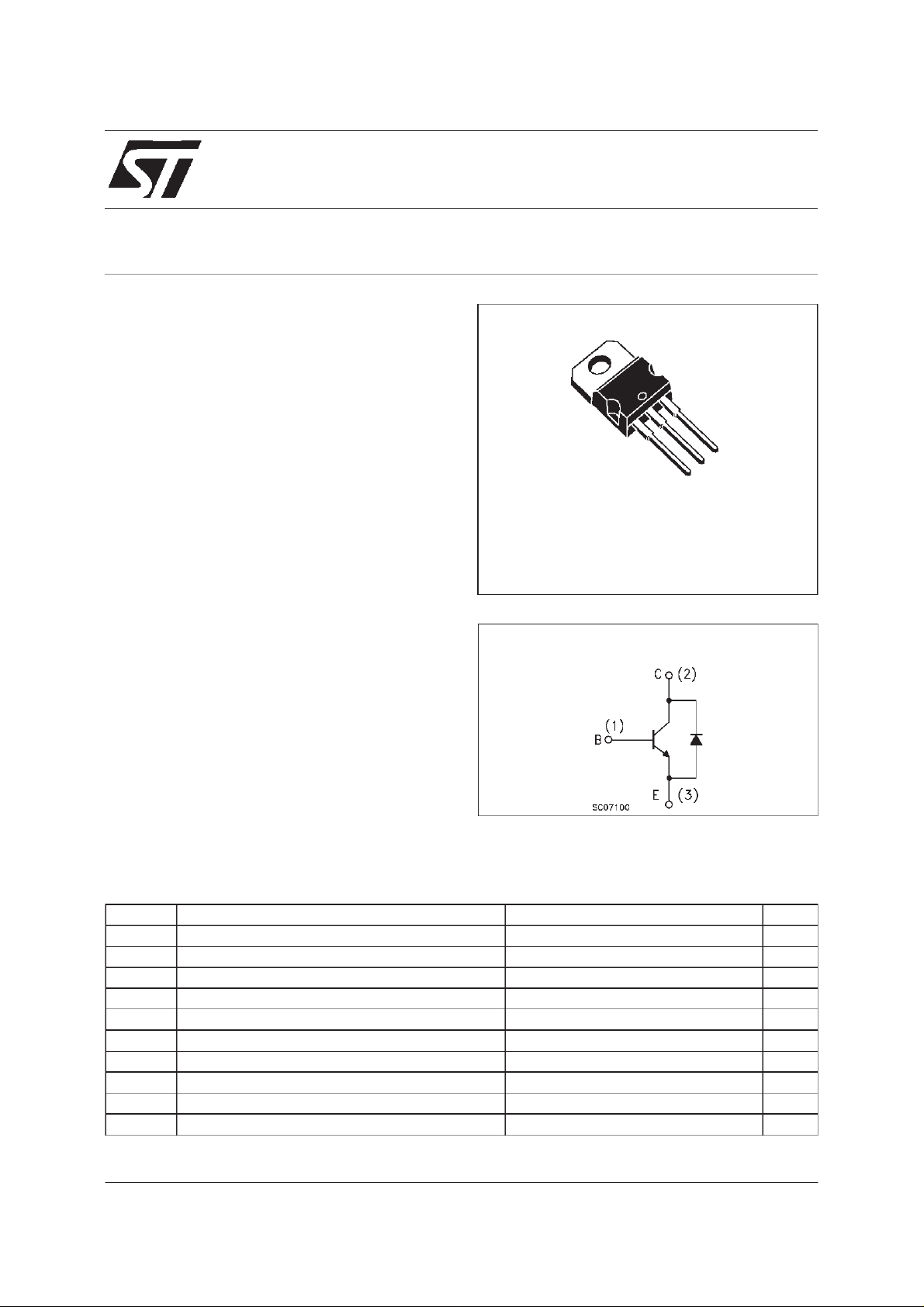
BUL128D-B
NPN POWER TRANSISTOR
3
2
1
APPLICATIONS:
■ ELECTRONICBALLASTSFOR
TO-220
FLUORESCENT LIGHTING
■ FLYBACKAND FORWARDSINGLE
TRANSISTOR LOW POWER CONVERTERS
DESCRIPTION
The device is manufactured using high voltage
INTERNAL SCHEMATIC DIAGRAM
Multi Epitaxial Planar technology for high
switchingspeeds and medium voltage capability.
It uses a Cellular Emitter structure with planar
edge termination to enhance switching speeds
while maintaining the wide RBSOA.
The device is designed for use in lighting
applications and low cost switch-mode power
supplies.
ABSOLUTE MAXIMUM RATINGS
Symbol Parameter Value Unit
V
V
V
I
I
P
T
Collect or-Emit t e r Voltage (VBE= 0) 700 V
CES
Collect or-Emit t e r Voltage (IB= 0) 400 V
CEO
Emitter-Base Voltage (IC=0) 9 V
EBO
Collect or Current 4 A
I
C
Collect or Peak Current (tp<5ms) 8 A
CM
Base Current 2 A
I
B
Base Pea k Curre nt (tp<5ms) 4 A
BM
Tot al Dissipation at Tc=25oC70W
tot
Storage Temperature -65 to 150
stg
Max. Ope r ating Junc tion Tem pe r ature 150
T
j
o
C
o
C
November 1998
1/7
Page 2
BUL128D-B
THERMAL DATA
R
thj-case
R
thj-amb
Ther mal Resist an c e Junction-Case Max
Ther mal Resist an c e Junction-Ambient Max
1.78
62.5
o
C/W
o
C/W
ELECTRICAL CHARACTERISTICS (T
=25oC unlessotherwise specified)
case
Symbol Parameter Test Cond itions Min. Typ. Max. Unit
I
CES
I
CEO
V
EBO
V
CEO(sus)
Collec t or Cut -off
Current (V
=-1.5V)
BE
Collec t or Cut -off
Current (I
B
=0)
Emitter-Base Voltage IE=10mA 9 V
Collec t or -Emitt er
V
=700V
CE
=700V Tj= 125oC
V
CE
V
= 400 V 250 µA
CE
100
500
IC= 100 m A L = 25 mH 400 V
Sust aining V o lt age
∗ Collector-E mitter
V
CE(sat)
Saturation Voltage
V
∗ Base-Emitt er
BE(sat)
Saturation Voltage
h
∗ DC C ur r ent Gain IC=10mA VCE=5V
FE
V
For ward V o lt age Drop If=2 A 2.5 V
f
INDUCTIV E LOAD
t
s
t
f
Storage Ti me
Fall Time
IC=0.5A IB=0.1A
=1A IB=0.2A
I
C
=2.5A IB=0.5A
I
C
=4A IB=1A 0.5
I
C
IC=0.5A IB=0.1A
=1A IB=0.2A
I
C
=2.5A IB=0.5A
I
C
=2A VCE=5V
I
C
VCC=200 V IC=2A
I
=0.4A V
B1
=0Ω L=200 µH
R
BB
BE(off)
=-5V
10
840
0.6
0.1
0.7
1.0
1.5
1.1
1.2
1.3
(see fig.1)
RESI STIVE LO AD
t
∗
Pulsed: Pulse duration = 300 µs, duty cycle 1.5 %
s
t
f
Storage Ti me
Fall Time
VCC=250V IC=2A
=0.4A IB2=-0.4A
I
B1
=30µs(seefig.2)
T
p
2
0.2
2.9 µs
µA
µA
V
V
V
V
V
V
V
µs
µs
µs
2/7
Page 3
BUL128D-B
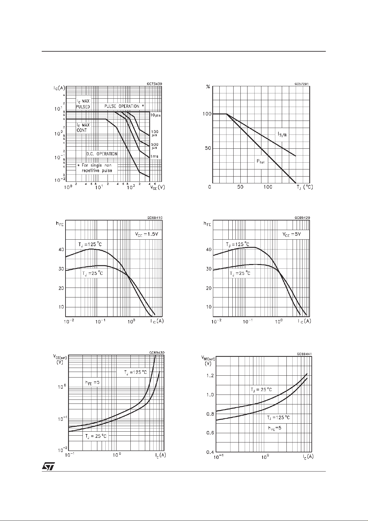
Safe Operating Areas
DCCurrent Gain
DeratingCurve
DC Current Gain
CollectorEmitterSaturationVoltage
BaseEmitterSaturation Voltage
3/7
Page 4

BUL128D-B
InductiveFall Time InductiveStorage Time
ResistiveLoad Fall Time Resistive Load Storage Time
ReverseBiased SOA
4/7
Page 5

Figure1: InductiveLoad Switching TestCircuits.
1) Fast elect r on ic switc h
2) Non-inductive Resistor
3) Fast recovery rectifier
Figure2: ResistiveLoadSwitching Test Circuits.
BUL128D-B
1) Fast elect r on ic switc h
2) Non-inductive Resistor
5/7
Page 6

BUL128D-B
TO-220 MECHANICAL DATA
DIM.
MIN. TYP. MAX. MIN. TYP. MAX.
A 4.40 4.60 0.173 0.181
C 1.23 1.32 0.048 0.051
D 2.40 2.72 0.094 0.107
D1 1.27 0.050
E 0.49 0.70 0.019 0.027
F 0.61 0.88 0.024 0.034
F1 1.14 1.70 0.044 0.067
F2 1.14 1.70 0.044 0.067
G 4.95 5.15 0.194 0.203
G1 2.4 2.7 0.094 0.106
H2 10.0 10.40 0.393 0.409
L2 16.4 0.645
L4 13.0 14.0 0.511 0.551
L5 2.65 2.95 0.104 0.116
L6 15.25 15.75 0.600 0.620
L7 6.2 6.6 0.244 0.260
L9 3.5 3.93 0.137 0.154
DIA. 3.75 3.85 0.147 0.151
mm inch
6/7
P011C
Page 7

BUL128D-B
Information furnished is believed to be accurate and reliable. However, STMicroelectronics assumes no responsibility for the consequences
of use of such information nor for any infringement of patents or other rights of third parties which may result from its use. No license is
granted by implication or otherwise under any patent or patent rights of STMicroelectronics. Specification mentioned in this publication are
subject to change without notice. This publication supersedes and replaces all information previously supplied. STMicroelectronics products
are not authorized for use as critical components in life support devices or systems without express written approval of STMicroelectronics.
The ST logo is a registered trademark of STMicroelectronics
1998 STMicroelectronics – Printed in Italy – All Rights Reserved
STMicroelectronicsGROUP OF COMPANIES
Australia - Brazil - Canada- China - France - Germany - Italy - Japan - Korea - Malaysia - Malta -Mexico - Morocco - The Netherlands -
Singapore - Spain - Sweden - Switzerland - Taiwan - Thailand - UnitedKingdom - U.S.A.
http://www.st.com
.
7/7
 Loading...