

Page 1

Philips Semiconductors Product specification
TrenchMOS transistor BUK7830-30
Standard level FET
GENERAL DESCRIPTION QUICK REFERENCE DATA
N-channel enhancement mode SYMBOL PARAMETER MAX. UNIT
standard level field-effect power
transistor in a plastic envelope V
suitable for surface mounting. Using I
DS
D
’trench’ technology, the device Drain current (DC) T
featuresverylow on-state resistance P
and has integral zener diodes giving T
ESD protection up to 2kV. It is R
tot
j
DS(ON)
intended for use in automotive and resistance VGS = 10 V
general purpose switching
applications.
PINNING - SOT223 PIN CONFIGURATION SYMBOL
Drain-source voltage 30 V
Drain current (DC) Tsp = 25 ˚C 12.8 A
= 25 ˚C 5.9 A
amb
Total power dissipation 8.3 W
Junction temperature 150 ˚C
Drain-source on-state 30 mΩ
PIN DESCRIPTION
4
d
1 gate
2 drain
3 source
4 drain (tab)
1
23
g
s
LIMITING VALUES
Limiting values in accordance with the Absolute Maximum System (IEC 134)
SYMBOL PARAMETER CONDITIONS MIN. MAX. UNIT
V
V
±V
I
D
I
D
I
DM
P
T
DS
DGR
tot
stg
GS
, T
j
Drain-source voltage - - 30 V
Drain-gate voltage RGS = 20 kΩ -30V
Gate-source voltage - - 16 V
Drain current (DC) T
= 25 ˚C - 12.8 A
sp
T
= 25 ˚C - 5.9 A
amb
Drain current (DC) Tsp = 100 ˚C - 9 A
T
= 100 ˚C - 4.1 A
amb
Drain current (pulse peak value) Tsp = 25 ˚C - 51.2 A
T
= 25 ˚C - 23.6 A
amb
Total power dissipation Tsp = 25 ˚C - 8.3 W
T
= 25 ˚C - 1.8 W
amb
Storage & operating temperature - - 55 150 ˚C
THERMAL RESISTANCES
SYMBOL PARAMETER CONDITIONS TYP. MAX. UNIT
R
th j-sp
R
th j-amb
December 1997 1 Rev 1.100
Thermal resistance junction to Mounted on any PCB 12 15 K/W
solder point
Thermal resistance junction to Mounted on PCB of Fig.19 - 70 K/W
ambient
Page 2

Philips Semiconductors Product specification
TrenchMOS transistor BUK7830-30
Standard level FET
ESD LIMITING VALUE
SYMBOL PARAMETER CONDITIONS MIN. MAX. UNIT
V
C
STATIC CHARACTERISTICS
Tj= 25˚C unless otherwise specified
SYMBOL PARAMETER CONDITIONS MIN. TYP. MAX. UNIT
V
(BR)DSS
V
GS(TO)
I
DSS
I
GSS
±V
(BR)GSS
R
DS(ON)
Electrostatic discharge capacitor Human body model - 2 kV
voltage, all pins (100 pF, 1.5 kΩ)
Drain-source breakdown VGS = 0 V; ID = 0.25 mA; 30 - - V
voltage Tj = -55˚C 27 - - V
Gate threshold voltage VDS = VGS; ID = 1 mA 2.0 3.0 4.0 V
Tj = 150˚C 1.0 - - V
Tj = -55˚C - - 4.4
Zero gate voltage drain current VDS = 30 V; VGS = 0 V; - 0.05 10 µA
Tj = 150˚C - - 500 µA
Gate source leakage current VGS = ±10 V; VDS = 0 V - 0.02 1 µA
Tj = 150˚C - - 20 µA
Gate source breakdown voltage IG = ±1 mA; 16 - - V
Drain-source on-state VGS = 10 V; ID = 3.2 A - 24 30 mΩ
resistance Tj = 150˚C - - 51 mΩ
DYNAMIC CHARACTERISTICS
Tj = 25˚C unless otherwise specified
SYMBOL PARAMETER CONDITIONS MIN. TYP. MAX. UNIT
g
Q
Q
Q
C
C
C
t
t
t
t
L
L
L
fs
g(tot)
gs
gd
iss
oss
rss
d on
r
d off
f
d
d
s
Forward transconductance VDS = 25 V; ID = 5.9 A 5 10 - S
Total gate charge ID = 5.9 A; V
= 24 V; VGS = 10 V - 22.5 - nC
DD
Gate-source charge - 4.5 - nC
Gate-drain (Miller) charge - 9 - nC
Input capacitance VGS = 0 V; VDS = 25 V; f = 1 MHz - 740 - pF
Output capacitance - 270 - pF
Feedback capacitance - 130 - pF
Turn-on delay time VDD = 15 V; ID = 5.9 A; - 16 22 ns
Turn-on rise time VGS = 10 V; RG = 5 Ω - 3060ns
Turn-off delay time Resistive load - 35 50 ns
Turn-off fall time - 25 38 ns
Internal drain inductance Measured from contact screw on - 3.5 - nH
tab to centre of die
Internal drain inductance Measured from drain lead 6 mm - 4.5 - nH
from package to centre of die
Internal source inductance Measured from source lead 6 mm - 7.5 - nH
from package to source bond pad
December 1997 2 Rev 1.100
Page 3

Philips Semiconductors Product specification
TrenchMOS transistor BUK7830-30
Standard level FET
REVERSE DIODE LIMITING VALUES AND CHARACTERISTICS
Tj = 25˚C unless otherwise specified
SYMBOL PARAMETER CONDITIONS MIN. TYP. MAX. UNIT
I
DR
I
DRM
V
SD
t
rr
Q
rr
AVALANCHE LIMITING VALUE
SYMBOL PARAMETER CONDITIONS MIN. TYP. MAX. UNIT
W
DSS
Continuous reverse drain - - 6.2 A
current
Pulsed reverse drain current - - 24.8 A
Diode forward voltage IF = 3.2 A; VGS = 0 V - 0.75 1.2 V
IF = 5.9 A; VGS = 0 V - 0.85 -
Reverse recovery time IF = 5.9 A; -dIF/dt = 100 A/µs; - 115 - ns
Reverse recovery charge VGS = -10 V; VR = 25 V - 0.3 - µC
Drain-source non-repetitive ID = 5.9 A; VDD ≤ 25 V; - - 60 mJ
unclamped inductive turn-off VGS = 10 V; RGS = 50 Ω; Tsp = 25 ˚C
energy
December 1997 3 Rev 1.100
Page 4
Philips Semiconductors Product specification
TrenchMOS transistor BUK7830-30
Standard level FET
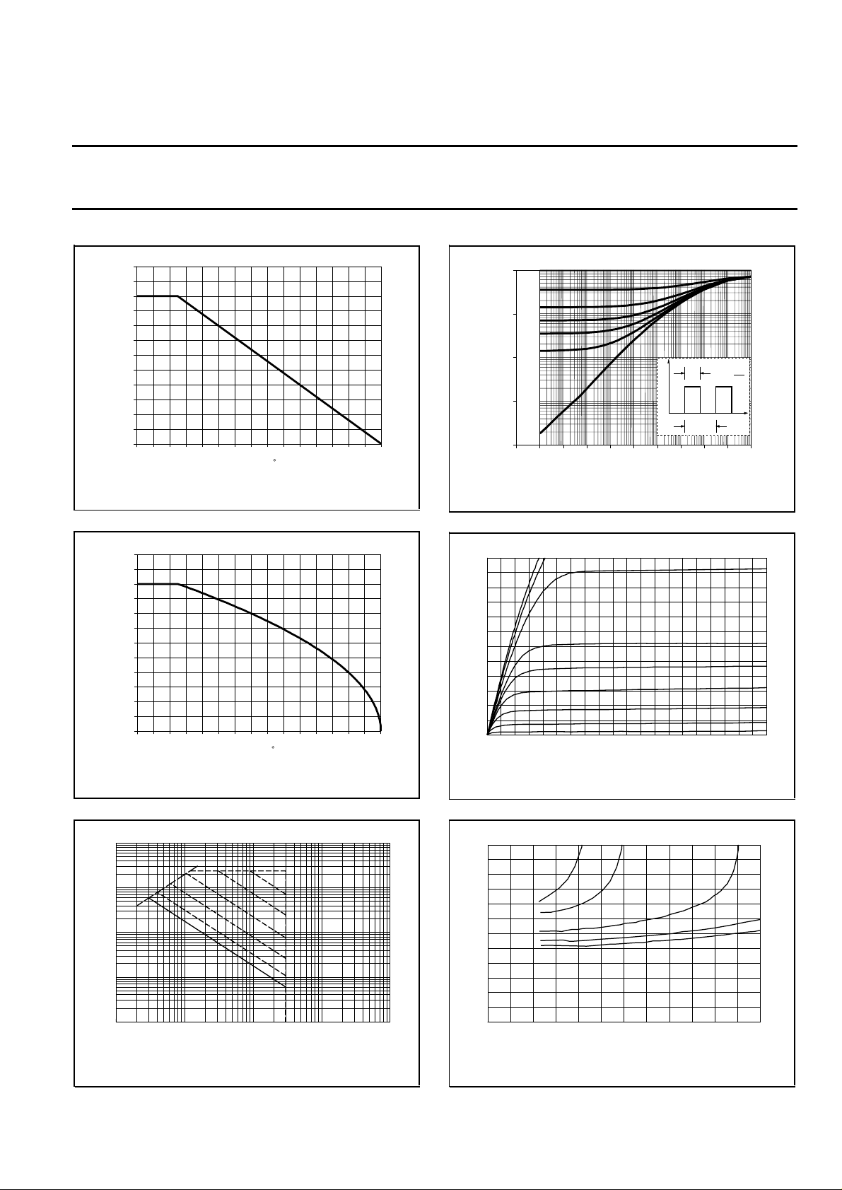
PD%
120
110
100
90
80
70
60
50
40
30
20
10
0
0 20 40 60 80 100 120 140
Normalised Power Derating
Tmb / C
Fig.1. Normalised power dissipation.
PD% = 100⋅PD/P
ID%
120
110
100
90
80
70
60
50
40
30
20
10
0
0 20 40 60 80 100 120 140
Tmb / C
= f(Tmb)
D 25 ˚C
Normalised Current Derating
Fig.2. Normalised continuous drain current.
ID% = 100⋅ID/I
= f(Tmb); conditions: VGS ≥ 10 V
D 25 ˚C
t
p
T
BUKX83
t
D =
T
p
t
Zth j-amb / (K/W)
1E+02
D =
0.5
1E+01
1E+00
0.2
0.1
0.05
0.02
P
D
1E-01
1E-02
0
1E-07 1E-05 1E-03 1E-01 1E+01 1E+03
t / s
Fig.4. Transient thermal impedance.
Z
= f(t); parameter D = tp/T
th j-mb
ID / A
60
50
40
30
20
10
0
0246810
1012
VGS / V =
VDS / V
Fig.5. Typical output characteristics, Tj = 25 ˚C
ID = f(VDS); parameter V
BUK7830-30
GS
6.5
5.5
4.5
8
6
5
4
.
ID / A
100
10
RDS(ON) = VDS / ID
1
DC
0.1
0.01
0.1 1 10 100 1000
VDS / V
tp = 10 us
100 us
1 ms
10 ms
100 ms
7830-30
Fig.3. Safe operating area. Tmb = 25 ˚C
ID & IDM = f(VDS); IDM single pulse; parameter t
p
RDS(ON) / mOhm
6
5
4
3
2
1
0
0 102030405060
VGS / V =
ID / A
Fig.6. Typical on-state resistance, Tj = 25 ˚C
R
= f(ID); parameter V
DS(ON)
7830-30
86.56
10
12
.
GS
December 1997 4 Rev 1.100
Page 5
Philips Semiconductors Product specification
TrenchMOS transistor BUK7830-30
Standard level FET
ID / A
60
50
40
30
20
10
0
0246810
VGS / V
Tj / C = 25
7830-30
150
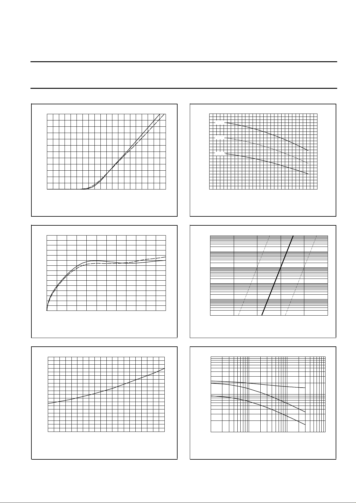
Fig.7. Typical transfer characteristics.
ID = f(VGS) ; conditions: VDS = 25 V; parameter T
15
10
gfs / S
Tj / C = 25
150
5
7830-30
j
VGS(TO) / V
5
max.
4
typ.
3
min.
2
1
0
-100 -50 0 50 100 150 200
Tj / C
BUK759-60
Fig.10. Gate threshold voltage.
V
= f(Tj); conditions: ID = 1 mA; VDS = V
GS(TO)
1E-01
1E-02
1E-03
1E-04
2%
Sub-Threshold Conduction
typ
98%
GS
0
0 102030405060
Fig.8. Typical transconductance, Tj = 25 ˚C
ID / A
.
gfs = f(ID); conditions: VDS = 25 V
a
2
1.5
1
0.5
0
-50 0 50 100 150
SOT223 30V Trench
Normalised RDS(ON) = f(Tj)
Tj / C
Fig.9. Normalised drain-source on-state resistance.
a = R
DS(ON)/RDS(ON)25 ˚C
= f(Tj); ID = 3.2 A; VGS = 10 V
1E-05
1E-06
012345
Fig.11. Sub-threshold drain current.
ID = f(V
C / pF
10000
1000
100
0.1 1 10 100
Fig.12. Typical capacitances, C
; conditions: Tj = 25 ˚C; VDS = V
GS)
VDS / V
, C
iss
7528-30
, C
oss
GS
Ciss
Coss
Crss
rss
.
C = f(VDS); conditions: VGS = 0 V; f = 1 MHz
December 1997 5 Rev 1.100
Page 6
Philips Semiconductors Product specification
TrenchMOS transistor BUK7830-30
Standard level FET
VGS / V
10
8
6
4
2
0
0 5 10 15 20 25
VDS / V = 6 24
QG / nC
7830-30
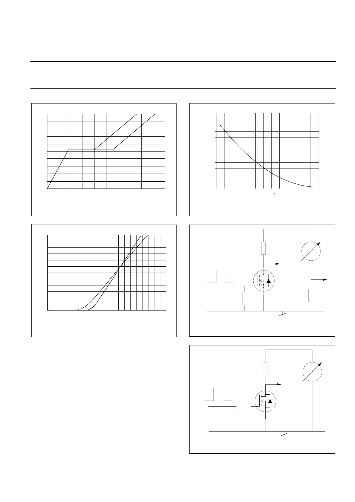
Fig.13. Typical turn-on gate-charge characteristics.
V
= f(QG); conditions: ID = 5.9 A; parameter V
GS
IF / A
60
50
40
30
20
10
0
0 0.5 1 1.5 2
Tj / C = 150
25
VSDS / V
DS
7830-30
Fig.14. Typical reverse diode current.
IF = f(V
); conditions: V
SDS
= 0 V; parameter T
GS
j
WDSS%
120
110
100
90
80
70
60
50
40
30
20
10
0
20 40 60 80 100 120 140
Tmb / C
Fig.15. Normalised avalanche energy rating.
W
% = f(Tmb); conditions: ID = 5.9 A
DSS
+
L
VDS
VGS
0
RGS
T.U.T.
Fig.16. Avalanche energy test circuit.
W
= 0.5 ⋅ LI
DSS
2
D
⋅BV
DSS
/(BV
DSS−VDD
-
R 01
shunt
)
VDD
-ID/100
VDD
+
RD
VDS
VGS
0
RG
T.U.T.
-
Fig.17. Switching test circuit.
December 1997 6 Rev 1.100
Page 7
Philips Semiconductors Product specification
TrenchMOS transistor BUK7830-30
Standard level FET
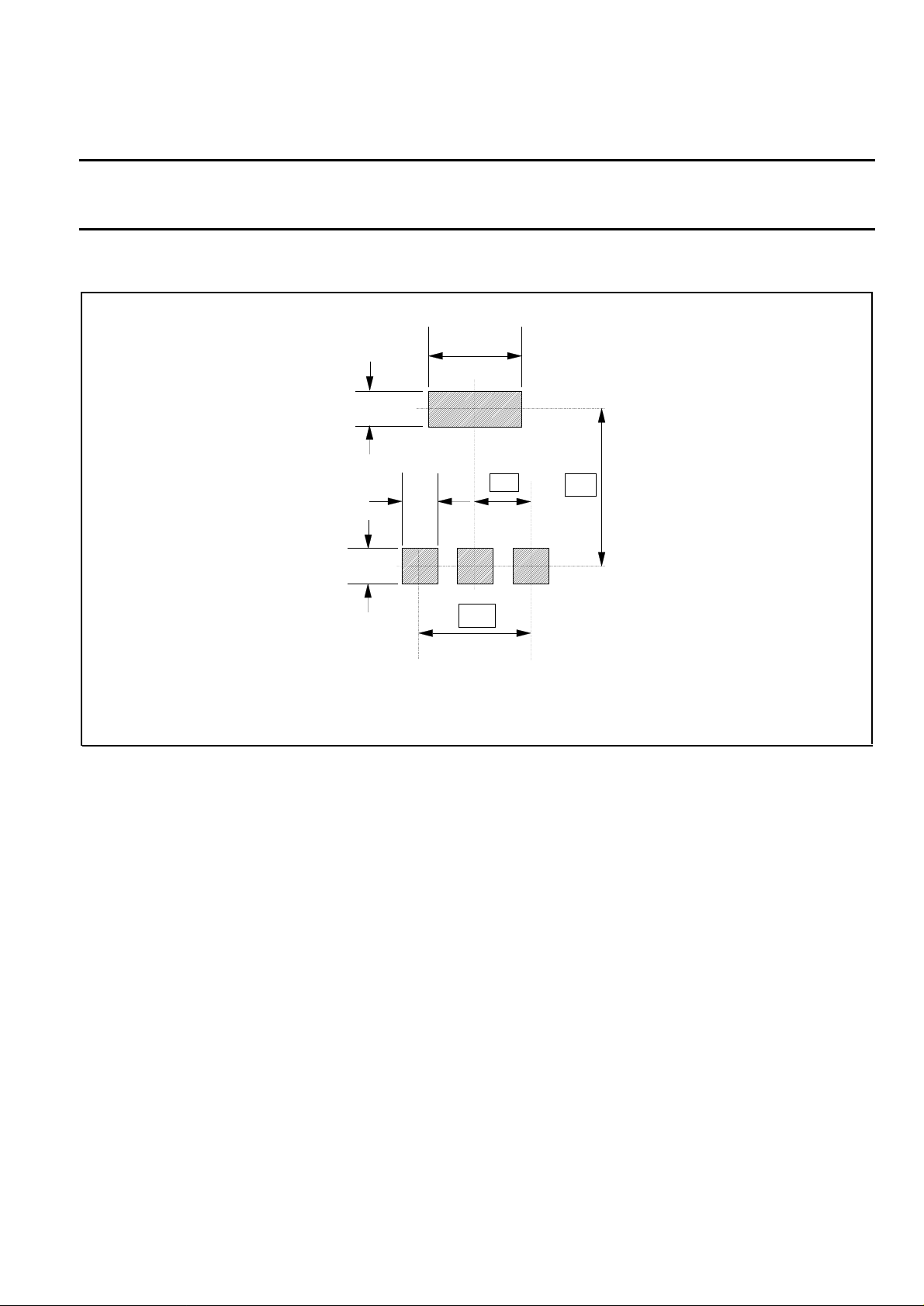
MOUNTING INSTRUCTIONS
Dimensions in mm.
3.8
min
1.5
min
Fig.18. soldering pattern for surface mounting SOT223.
PRINTED CIRCUIT BOARD
1.5
min
1.5
min
(3x)
4.6
2.3
6.3
December 1997 7 Rev 1.100
Page 8
Philips Semiconductors Product specification
TrenchMOS transistor BUK7830-30
Standard level FET
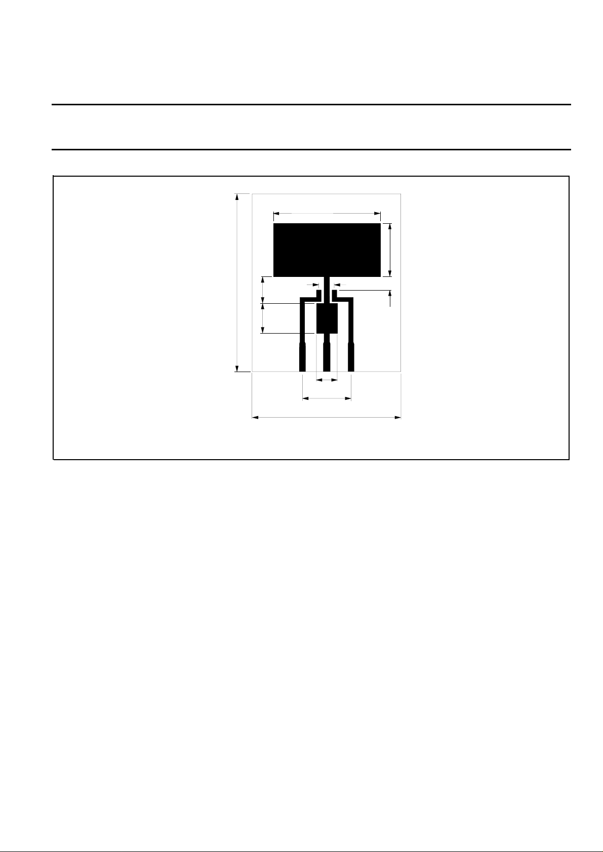
Dimensions in mm.
36
18
60
4.6
9
10
7
50
15
4.5
Fig.19. PCB for thermal resistance and power rating for SOT223.
PCB: FR4 epoxy glass (1.6 mm thick), copper laminate (35 µm thick).
December 1997 8 Rev 1.100
Page 9
Philips Semiconductors Product specification
TrenchMOS transistor BUK7830-30
Standard level FET
MECHANICAL DATA
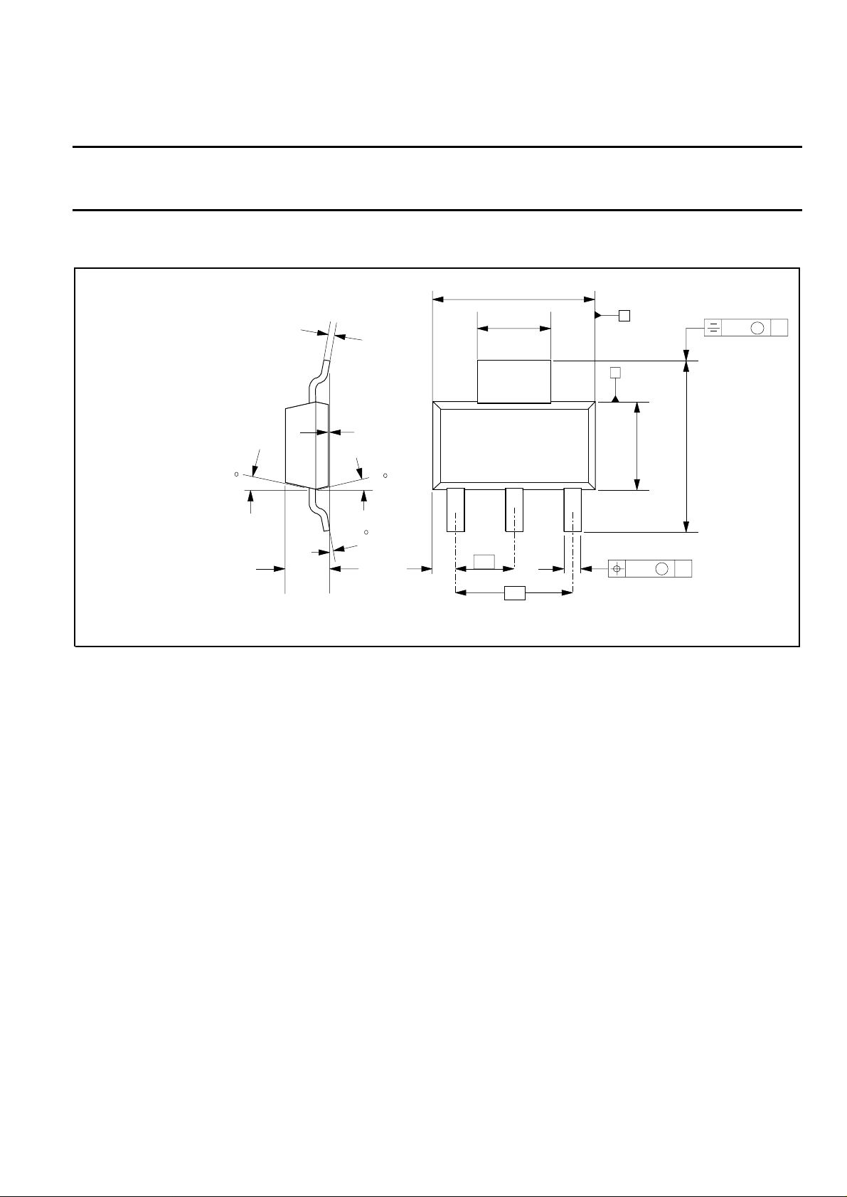
Dimensions in mm
Net Mass: 0.11 g
16
max
1.8
max
0.32
0.24
0.10
0.02
10
max
13
1.05
0.85
6.7
6.3
3.1
2.9
4
1
2.3
23
0.80
0.60
4.6
B
A
7.3
6.7
M
B
0.1
3.7
3.3
(4x)
Fig.20. SOT223 surface mounting package.
Notes
1. Observe the general handling precautions for electrostatic-discharge sensitive devices (ESDs) to prevent
damage to MOS gate oxide.
2. Refer to surface mounting instructions for SOT223 envelope.
3. Epoxy meets UL94 V0 at 1/8".
AM0.2
December 1997 9 Rev 1.100
Page 10

Philips Semiconductors Product specification
TrenchMOS transistor BUK7830-30
Standard level FET
DEFINITIONS
Data sheet status
Objective specification This data sheet contains target or goal specifications for product development.
Preliminary specification This data sheet contains preliminary data; supplementary data may be published later.
Product specification This data sheet contains final product specifications.
Limiting values
Limiting values are given in accordance with the Absolute Maximum Rating System (IEC 134). Stress above one
or more of the limiting values may cause permanent damage to the device. These are stress ratings only and
operation of the device at these or at any other conditions above those given in the Characteristics sections of
this specification is not implied. Exposure to limiting values for extended periods may affect device reliability.
Application information
Where application information is given, it is advisory and does not form part of the specification.
Philips Electronics N.V. 1997
All rights are reserved. Reproduction in whole or in part is prohibited without the prior written consent of the
copyright owner.
The information presented in this document does not form part of any quotation or contract, it is believed to be
accurate and reliable and may be changed without notice. No liability will be accepted by the publisher for any
consequence of its use. Publication thereof does not convey nor imply any license under patent or other
industrial or intellectual property rights.
LIFE SUPPORT APPLICATIONS
These products are not designed for use in life support appliances, devices or systems where malfunction of these
products can be reasonably expected to result in personal injury. Philips customers using or selling these products
for use in such applications do so at their own risk and agree to fully indemnify Philips for any damages resulting
from such improper use or sale.
December 1997 10 Rev 1.100
 Loading...