

Page 1

查询BUK1M200_50SDLD供应商
BUK1M200-50SDLD
Quad channel TOPFET™
Rev. 01 — 02 April 2003 Product data
1. Product profile
1.1 Description
Quad temperature and overload protected logic level power MOSFET in TOPFET™
technology in a 20-pin surface mount plastic package.
Product availability:
BUK1M200-50SDLD in SOT163-1 (SO20).
1.2 Features
■ Power TrenchMOS™ ■ 5 V logic compatible input level
■ Overtemperature protection ■ Current limiting
■ Overload protection ■ ESD protection for all pins
■ Input-source voltage resets latched
protection circuitry.
■ Input used to control output stage and
supply overload protection circuits
■ Overfatigue clamping for turn off of
inductive loads
■ Low operating input current permits
direct drive by micro-controller.
1.3 Applications
■ Low-side driver ■ DC switching
■ Low frequency Pulse Width
Modulation
■ General purpose switch for driving
lamps, motors, solenoids and heaters.
1.4 Quick reference data
Table 1: Quick reference data
Symbol Parameter Min Max Unit
R
DSon
P
tot
T
j
V
DS
[1] All devices active
drain-source on-state resistance - 200 mΩ
total power dissipation
junction temperature - 150 °C
drain-source voltage - 50 V
[1]
- 9.4 W
Page 2
Philips Semiconductors
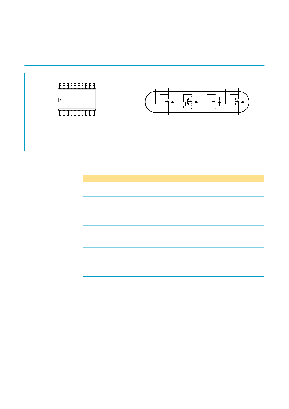
2. Pinning information
BUK1M200-50SDLD
Quad channel TOPFET™
book, halfpage
20
110
Top view
MGX361
11
D1I1
P
S1
D2I2
P
S2
D3I3
P
S3
Fig 1. Pinning; SOT163-1 (SO20). Fig 2. Symbol; Quad channel low-side TOPFET
2.1 Pin description
Table 2: Pin description
Symbol Pin Description
n.c. 1, 11, 10, 20 not connected
D1 2,19 drain 1
I1 3 input 1
D2 4,17 drain 2
I2 5 input 2
D3 6,15 drain 3
I3 7 input 3
D4 8, 13 drain 4
I4 9 input 4
S4 12 source 4
S3 14 source 3
S2 16 source 2
S1 18 source 1
D4I4
P
S4
MBL801
TM
9397 750 10956
Product data Rev. 01 — 02 April 2003 2 of 14
© Koninklijke Philips Electronics N.V. 2003. All rights reserved.
Page 3
Philips Semiconductors
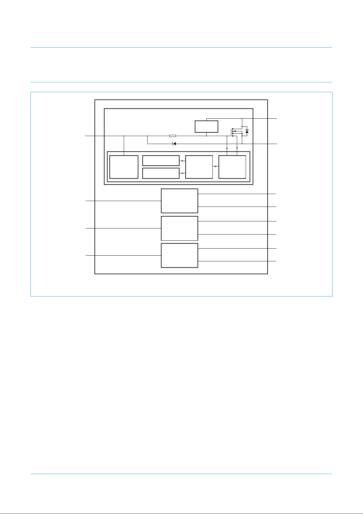
3. Block diagram
BUK1M200-50SDLD
Quad channel TOPFET™
2,19
CHANNEL 1
I1
3
SHORT CIRCUIT
VOLTAGE
REGULATOR
5
I2
7
I3
9
I4
PROTECTION
TEMPERATURE
R
OVER
CHANNEL 2
internal circuitry
identical to
CHANNEL1
CHANNEL 3
internal circuitry
identical to
CHANNEL1
CHANNEL 4
internal circuitry
identical to
CHANNEL1
IG
OVER
VOLTAGE
CONTROL
LOGIC
18
gate sense
CROWBAR
AND
CURRENT
LIMIT
4,17
16
6,15
14
8,13
12
D1
S1
D2
S2
D3
S3
D4
S4
BUK1M200-50SDLD
03pb05
Fig 3. Elements of the quad channel TOPFET switch.
9397 750 10956
© Koninklijke Philips Electronics N.V. 2003. All rights reserved.
Product data Rev. 01 — 02 April 2003 3 of 14
Page 4

Philips Semiconductors
BUK1M200-50SDLD
Quad channel TOPFET™
4. Limiting values
Table 3: Limiting values
In accordance with the Absolute Maximum Rating System (IEC 60134).
Symbol Parameter Conditions Min Max Unit
V
I
P
I
T
T
DS
I
tot
IMS
stg
j
drain-source voltage
input current clamping - 3 mA
total power dissipation Tsp≤ 25 °C; Figure 4
non-repetitive peak input current tp≤ 1 ms - 10 mA
storage temperature −55 +150 °C
junction temperature normal operation
Overvoltage clamping
E
DS(CL)S
non-repetitive drain-source
clamping energy
E
DS(CL)R
repetitive drain-source clamping
energy
Overload protection
V
DS(prot)
protected drain-source voltage VIS≥ 4V - 35 V
[6]
Reverse diode
I
S
source (diode forward) current Tsp≤ 25 °C; VIS=0V - 2 A
Electrostatic discharge
V
esd
electrostatic discharge voltage C = 250 pF; R = 1.5 kΩ -2kV
[4]
T
=25°C; IDM≤ I
amb
(refer to Table 5);
D(lim)
inductive load
Tsp≤ 125 °C; IDM= 50 mA; f = 250 Hz
[1]
-50V
[2]
- 9.4 W
[3]
- 150 °C
[5]
- 100 mJ
[5]
-5mJ
[1] Prior to the onset of overvoltage clamping. For voltages above this value, safe operation is limited by the overvoltage clamping energy.
[2] For all devices active.
[3] Not in an overload condition with drain current limiting.
[4] At a drain-source voltage above 50 V the power MOSFET is actively turned on to clamp overvoltage transients.
[5] Single active device.
[6] With the protectionsupply provided via the input pin, the TOPFET is protected from short circuit loads. Overload protection operates by
means of drain current limiting and by activating the overtemperature protection.
9397 750 10956
Product data Rev. 01 — 02 April 2003 4 of 14
© Koninklijke Philips Electronics N.V. 2003. All rights reserved.
Page 5
Philips Semiconductors
BUK1M200-50SDLD
Quad channel TOPFET™
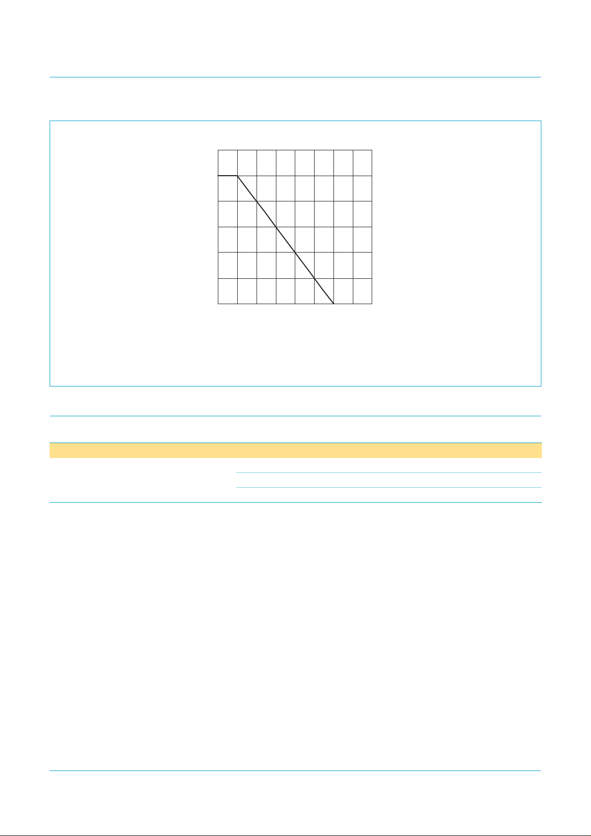
120
P
der
(%)
80
40
0
0 50 100 150 200
P
tot
P
der
-----------------------
P
tot 25 C°()
100%×=
03aa17
Tsp (°C)
Fig 4. Normalized total power dissipation as a function of solder point temperature.
5. Thermal characteristics
Table 4: Thermal characteristics
Symbol Parameter Conditions Min Typ Max Unit
R
th(j-sp)
thermal resistancefrom junction to
solder point.
mounted on thermo clad board
one device active - - 45 K/W
all devices active - - 13.3 K/W
9397 750 10956
Product data Rev. 01 — 02 April 2003 5 of 14
© Koninklijke Philips Electronics N.V. 2003. All rights reserved.
Page 6

Philips Semiconductors
BUK1M200-50SDLD
Quad channel TOPFET™
6. Static characteristics
Table 5: Static characteristics
Limits are valid for−40°C≤T
Symbol Parameter Conditions Min Typ Max Unit
Off-state output characteristics
V
DS(CL)
I
DSS
drain-source clamping voltage VIS=0V; ID=10mA 50 - - V
drain-source leakage current VIS=0V; VDS=40V - - 100 µA
On-state output characteristic
R
DSon
Input characteristics
V
IS(th)
I
IS
V
IS(rst)
t
rst(latch)
V
IS(CL)
R
IG
drain-source on-state resistance VIS≥ 4 V; tp≤ 300 µs; δ≤0.01;
[1]
input-source threshold voltage VDS=5V;ID= 1 mA 0.6 - 2.4 V
input-source current normal operation
input-source reset voltage t
latch reset time
input-source clamping voltage II= 1.5 mA; Figure 16 5.5 - 8.5 V
input-gate resistance
Overload protection characteristic
I
D(lim)
drain current limiting VIS=5V;Figure 18 0.8 1.3 1.7 A
Short circuit load protection characteristics
P
T
d(sc)
OV(th)
overload power threshold VIS=5V
short circuit response time VIS=5V;Figure 14
Overtemperature protection characteristic
T
j(th)
threshold junction temperature 4 V ≤ VIS≤ 5.5 V; ID≥ 280 mA or
Source-drain diode characteristic
V
SD
source-drain (diode forward)
voltage
≤
+150°C and typical values for Tsp=25°C unless otherwise specified.
sp
=0V; ID= 200 mA; tp≤ 300 µs;
V
IS
50 62 70 V
δ≤0.01; Figure 16
=25°C; Figure 17 - 0.05 10 µA
T
sp
- - 380 mΩ
= 100 mA; Figure 5 and 6
I
D
T
=25°C - 150 200 mΩ
sp
=25C;Figure 10 1.1 1.6 2.1 V
T
sp
= 5 V 100 220 400 µA
V
IS
= 4 V 80 195 330 µA
V
IS
protection latched
= 5 V 200 400 650 µA
V
IS
=3V;Figure 11 and 12 130 250 430 µA
V
IS
≥ 100 µs; Figure 15
rst
[4]
= 4.5 V 0.7 - - A
V
IS
4V≤ V
≤ 5.5 V; 0.6 - 1.8 A
IS
[2]
1.5 2 2.9 V
[6]
10 40 100 µs
[3]
-33-kΩ
[5]
-17-W
[7]
- 1.6 - ms
150 165 - °C
≥ 100 mV; Figure 9
V
DS
IS= 2 A; VIS=0V; tp= 300 µs - 0.83 1.1 V
[1] The supply for the logic and overload protection is taken from the input.
[2] The input voltage below which the overload protection circuits will be reset.
[3] Not directly measurable from the device terminals.
9397 750 10956
Product data Rev. 01 — 02 April 2003 6 of 14
© Koninklijke Philips Electronics N.V. 2003. All rights reserved.
Page 7

Philips Semiconductors
BUK1M200-50SDLD
Quad channel TOPFET™
[4] The TOPFET switches off to protect itself when one of the overload thresholds is exceeded. It remains latched off until reset by the
input.
[5] Power threshold for protection to operate.
[6] To reset the latched state, the input-source voltage is reduced from 5 V to 1 V.
[7] Trip time t
varies with overload dissipation POV according to the formula t
(trip)
(trip)=td(sc)
/[POV/P
OV(th)
-1]
2.5
a
2
1.5
1
0.5
0
-50 0 50 100 150
R
DSon
=
a
----------------------------- -
R
DSon 25°C()
03pa71
Tj (°C)
Fig 5. Normalized drain-source on-state resistance
factor as a function of junction temperature.
1.6
(A)
1.2
I
D
V
IS
03pa74
= 7 V
6 V
5 V
500
R
DSon
(mΩ)
375
250
125
0
02468
T
=25°C; ID= 100 mA; tp= 300 µs
j
03pa73
VIS (V)
Fig 6. Drain-source on-state resistance as a function
of input-source voltage; typical values.
1.8
I
(A)
1.2
D
03pa75
0.8
0.4
0
0 102030
Tj=25°C; tp= 300 µsT
Fig 7. Output characteristics; drain current as a
function of drain-source voltage; typical values.
9397 750 10956
4 V
VDS (V)
0.6
0
02468
=25°C; VDS= 10 V; tp= 300 µs
j
VIS (V)
Fig 8. Transfer characteristics; drain current as a
function of input-source voltage; typical values.
© Koninklijke Philips Electronics N.V. 2003. All rights reserved.
Product data Rev. 01 — 02 April 2003 7 of 14
Page 8

Philips Semiconductors
BUK1M200-50SDLD
Quad channel TOPFET™
200
T
j(th)
(°C)
190
180
170
160
0246810
03pa76
VIS (V)
Fig 9. Overtemperature protection characteristic;
threshold junction temperature as a function of
input-source voltage; typical values.
03pa78
I
IS
(mA)
0.8
1
2.5
V
IS(th)
(V)
2
1.5
1
0.5
0
-50 0 50 100 150
max.
typ.
min.
03pa77
Tj (°C)
ID= mA; VDS=5V
Fig 10. Input-source threshold voltage as a function of
junction temperature.
10
I
(mA)
I
8
03pa79
0.6
0.4
0.2
0
02468
(1)
(2)
VIS (V)
Tj=25°C
(1) Protection latched.
(2) Normal operation.
Fig 11. Input-source current as a function of
input-source voltage; typical values.
6
4
2
0
02468
VIS (V)
Tj=25°C
Fig 12. Input clamping characteristic; input current as
a function of input-source voltage; typical
values.
9397 750 10956
© Koninklijke Philips Electronics N.V. 2003. All rights reserved.
Product data Rev. 01 — 02 April 2003 8 of 14
Page 9

Philips Semiconductors
BUK1M200-50SDLD
Quad channel TOPFET™
500
I
IS
(mA)
400
300
200
100
0
−50 0 50 100 150
(1)
(2)
(3)
(4)
03pa80
Tj (°C)
(1) VIS= 5 V; device in latched mode.
(2) VIS= 3 V; device in latched mode.
(3) VIS= 5 V; device in normal mode.
(4) VIS= 4 V; device in normal mode.
Fig 13. Input-source current as a function of junction
temperature; typical values.
4000
1 / t
d(sc)
(s-1)
3000
2000
1000
0
0 5.5 11 16.5 22
03pa81
POV (W)
VIS≥ 4 V; Tj≤ 125 °C
Fig 14. Reciprocal of short circuit response time as a
function of total overload power; single device
dissipating; typical values
2.4
V
IS(rst)
(V)
2.2
2
1.8
-50 20 90 160
03pa82
Tj (°C)
tr= 100 µsV
Fig 15. Input-source reset voltage as a function of
junction temperature; typical values.
400
I
D
(mA)
300
200
100
0
57 59 61 63 65 67
=0V; tp= 300 µs
IS
Fig 16. Overvoltage clamping characteristic; drain
current as a function of drain-source voltage;
03pa83
VDS (V)
typical values.
9397 750 10956
© Koninklijke Philips Electronics N.V. 2003. All rights reserved.
Product data Rev. 01 — 02 April 2003 9 of 14
Page 10

Philips Semiconductors
BUK1M200-50SDLD
Quad channel TOPFET™
-5
10
I
DSS
(A)
-6
10
-7
10
-8
10
-50 0 50 100 150
VDS=40V; VIS=0V V
Fig 17. Drain-source leakage current as a function of
junction temperature; typical values.
03pa84
Tj (°C)
1.8
I
D
(A)
1.2
0.6
0
0 40 80 120 160
=5V
IS
max.
typ.
min.
03pa72
Tsp (°C)
Fig 18. Drain current limiting as a function of solder
point temperature.
7. Dynamic characteristics
Table 6: Switching characteristics
Symbol Parameter Conditions Min Typ Max Unit
Turn-on measured from the input going HIGH
t
d(on)
t
r
t
d(off)
t
f
turn-on delay time RL=50Ω; ID= 250 mA; VIS=5V;
rise time - 11 30 µs
Figure 19 and 20; T
=25°C
sp
turn-off delay time - 25 65 µs
fall time -1435µs
-512µs
V
MBL853
DD
t
d(on)
R
L
V
DS
P
V
IS
V
DS
V
90%
10%
IS
10%
90%
t
f
t
d(off)
t
r
MBL854
Fig 19. Test circuit for resistive load switching times. Fig 20. Resistive load switching waveforms.
9397 750 10956
Product data Rev. 01 — 02 April 2003 10 of 14
© Koninklijke Philips Electronics N.V. 2003. All rights reserved.
Page 11

Philips Semiconductors
8. Package outline
BUK1M200-50SDLD
Quad channel TOPFET™
SO20: plastic small outline package; 20 leads; body width 7.5 mm
D
c
y
Z
20
pin 1 index
1
e
11
A
2
10
w M
b
p
SOT163-1
E
H
E
Q
A
1
L
p
L
detail X
(A )
A
X
v M
A
A
3
θ
0 5 10 mm
scale
DIMENSIONS (inch dimensions are derived from the original mm dimensions)
mm
OUTLINE
VERSION
SOT163-1
A
A1A2A3b
max.
0.30
2.65
0.10
0.012
0.10
0.004
p
2.45
2.25
0.096
0.089
IEC JEDEC EIAJ
075E04 MS-013
0.25
0.01
0.49
0.36
0.019
0.014
0.013
0.009
UNIT
inches
Note
1. Plastic or metal protrusions of 0.15 mm maximum per side are not included.
(1)E(1) (1)
cD
0.32
13.0
0.23
12.6
0.51
0.49
REFERENCES
eHELLpQ
7.6
7.4
0.30
0.29
1.27
0.050
10.65
10.00
0.419
0.394
1.4
0.055
1.1
0.4
0.043
0.016
1.1
1.0
0.043
0.039
0.25
0.01
EUROPEAN
PROJECTION
0.25 0.1
0.01
0.004
ywv θ
Z
0.9
0.4
0.035
0.016
ISSUE DATE
97-05-22
99-12-27
o
8
o
0
Fig 21. SOT163-1.
9397 750 10956
Product data Rev. 01 — 02 April 2003 11 of 14
© Koninklijke Philips Electronics N.V. 2003. All rights reserved.
Page 12

Philips Semiconductors
9. Revision history
Table 7: Revision history
Rev Date CPCN Description
01 20030402 - Product datasheet (9397 750 10956)
BUK1M200-50SDLD
Quad channel TOPFET™
9397 750 10956
Product data Rev. 01 — 02 April 2003 12 of 14
© Koninklijke Philips Electronics N.V. 2003. All rights reserved.
Page 13

Philips Semiconductors
Philips Semiconductors
10. Data sheet status
BUK1M200-50SDLD
BUK1M200-50SDLD
Quad channel TOPFET™
Quad channel TOPFET™
Level Data sheet status
I Objective data Development This data sheet contains data from the objective specification for product development. Philips
II Preliminary data Qualification Thisdata sheetcontains data from the preliminary specification. Supplementary data will be published
III Product data Production This data sheet contains data from the product specification. Philips Semiconductors reserves the
[1] Please consult the most recently issued data sheet before initiating or completing a design.
[2] The product status of the device(s) described in this data sheet may have changed since this data sheet was published. The latest information is available on the Internet at
URL http://www.semiconductors.philips.com.
[3] For data sheets describing multiple type numbers, the highest-level product status determines the data sheet status.
[1]
Product status
11. Definitions
Short-form specification — The data in a short-form specification is
extracted from a full data sheet with the same type number and title. For
detailed information see the relevant data sheet or data handbook.
Limiting values definition — Limiting values given are in accordance with
the Absolute Maximum Rating System (IEC 60134). Stress above one or
more of the limiting values may cause permanent damage to the device.
These are stress ratings only and operation of the device at these or at any
other conditions above those given in the Characteristics sections of the
specification is not implied. Exposure to limiting values for extended periods
may affect device reliability.
Application information — Applications that are described herein for any
of these products are for illustrative purposes only. Philips Semiconductors
make no representation or warranty that such applications will be suitable for
the specified use without further testing or modification.
[2][3]
Definition
Semiconductors reserves the right to change the specification in any manner without notice.
at a later date. Philips Semiconductors reserves the right to change the specification without notice, in
order to improve the design and supply the best possible product.
right to make changes at any time in order to improve the design, manufacturing and supply.Relevant
changes will be communicated via a Customer Product/Process Change Notification (CPCN).
customers using or selling these products for use in such applications do so
at their own risk and agree to fully indemnify Philips Semiconductors for any
damages resulting from such application.
Right to make changes — Philips Semiconductors reserves the right to
make changes in the products - including circuits, standard cells, and/or
software - described or contained herein in order to improve design and/or
performance. When the product is in full production (status ‘Production’),
relevant changes will be communicated via a Customer Product/Process
Change Notification (CPCN). Philips Semiconductors assumes no
responsibility or liability for the use of any of these products, conveys no
licence or title under any patent, copyright, or mask work right to these
products, and makes no representations or warranties that these products are
free from patent, copyright, ormask work right infringement, unless otherwise
specified.
13. Trademarks
12. Disclaimers
Life support — These products are not designed for use in life support
appliances, devices, or systems where malfunction of these products can
reasonably be expected to result in personal injury. Philips Semiconductors
TOPFET — is a trademark of Koninklijke Philips Electronics N.V.
TrenchMOS —is a trademark of Koninklijke Philips Electronics N.V.
Contact information
For additional information, please visit http://www.semiconductors.philips.com.
For sales office addresses, send e-mail to: sales.addresses@www.semiconductors.philips.com. Fax: +31 40 27 24825
© Koninklijke Philips Electronics N.V. 2003. All rights reserved.
9397 750 10956
9397 750 10956
Product data Rev. 01 — 02 April 2003 13 of 14
Product data Rev. 01 — 02 April 2003 13 of 14
© Koninklijke Philips Electronics N.V. 2003. All rights reserved.
Page 14

Philips Semiconductors
Contents
1 Product profile . . . . . . . . . . . . . . . . . . . . . . . . . . 1
1.1 Description . . . . . . . . . . . . . . . . . . . . . . . . . . . . 1
1.2 Features . . . . . . . . . . . . . . . . . . . . . . . . . . . . . . 1
1.3 Applications . . . . . . . . . . . . . . . . . . . . . . . . . . . 1
1.4 Quick reference data. . . . . . . . . . . . . . . . . . . . . 1
2 Pinning information. . . . . . . . . . . . . . . . . . . . . . 2
2.1 Pin description . . . . . . . . . . . . . . . . . . . . . . . . . 2
3 Block diagram . . . . . . . . . . . . . . . . . . . . . . . . . . 3
4 Limiting values. . . . . . . . . . . . . . . . . . . . . . . . . . 4
5 Thermal characteristics. . . . . . . . . . . . . . . . . . . 5
6 Static characteristics. . . . . . . . . . . . . . . . . . . . . 6
7 Dynamic characteristics . . . . . . . . . . . . . . . . . 10
8 Package outline . . . . . . . . . . . . . . . . . . . . . . . . 11
9 Revision history. . . . . . . . . . . . . . . . . . . . . . . . 12
10 Data sheet status. . . . . . . . . . . . . . . . . . . . . . . 13
11 Definitions . . . . . . . . . . . . . . . . . . . . . . . . . . . . 13
12 Disclaimers. . . . . . . . . . . . . . . . . . . . . . . . . . . . 13
13 Trademarks. . . . . . . . . . . . . . . . . . . . . . . . . . . . 13
BUK1M200-50SDLD
Quad channel TOPFET™
© Koninklijke Philips Electronics N.V. 2003.
Printed in The Netherlands
All rights are reserved. Reproduction in whole or in part is prohibited without the prior
written consent of the copyright owner.
The information presented in this document does not form part of any quotation or
contract, is believed to be accurate and reliable and may be changed without notice. No
liability will be accepted by the publisher for any consequence of its use. Publication
thereof does not convey nor imply any license under patent- or other industrial or
intellectual property rights.
Date of release: 02 April 2003 Document order number: 9397 750 10956
 Loading...