

Page 1
查询BUK114-50L供应商
Philips Semiconductors Product specification
Logic level TOPFET BUK114-50L/S
SMD version of BUK104-50L/S
DESCRIPTION QUICK REFERENCE DATA
Monolithic temperature and SYMBOL PARAMETER MAX. UNIT
overload protected logic level power
MOSFET in a 5 pin surface V
mounting plastic envelope, intended I
as a general purpose switch for P
automotive systems and other T
applications. R
DS
D
tot
j
DS(ON)
APPLICATIONS V
General controller for driving SYMBOL PARAMETER NOM. UNIT
lamps
motors V
solenoids BUK114-50L 5V
PSN
heaters BUK114-50S 10 V
FEATURES FUNCTIONAL BLOCK DIAGRAM
Continuous drain source voltage 50 V
Continuous drain current 15 A
Total power dissipation 40 W
Continuous junction temperature 150 ˚C
Drain-source on-state resistance
VIS = 5 V 125 mΩ
= 7 V 100 mΩ
IS
Protection supply voltage
Vertical power DMOS output
stage
Low on-state resistance
PROTECTION SUPPLY
Logic and protection supply
from separate pin
Low operating supply current
Overload protection against
over temperature
Overload protection against
short circuit load
FLAG
INPUT
O/V
CLAMP
Latched overload protection
reset by protection supply
Protection circuit condition
indicated by flag pin
5 V logic compatible input level
LOGIC AND
PROTECTION
Separate input pin
for higher frequency drive
ESD protection on input, flag
and protection supply pins
Over voltage clamping for turn
off of inductive loads
Both linear and switching
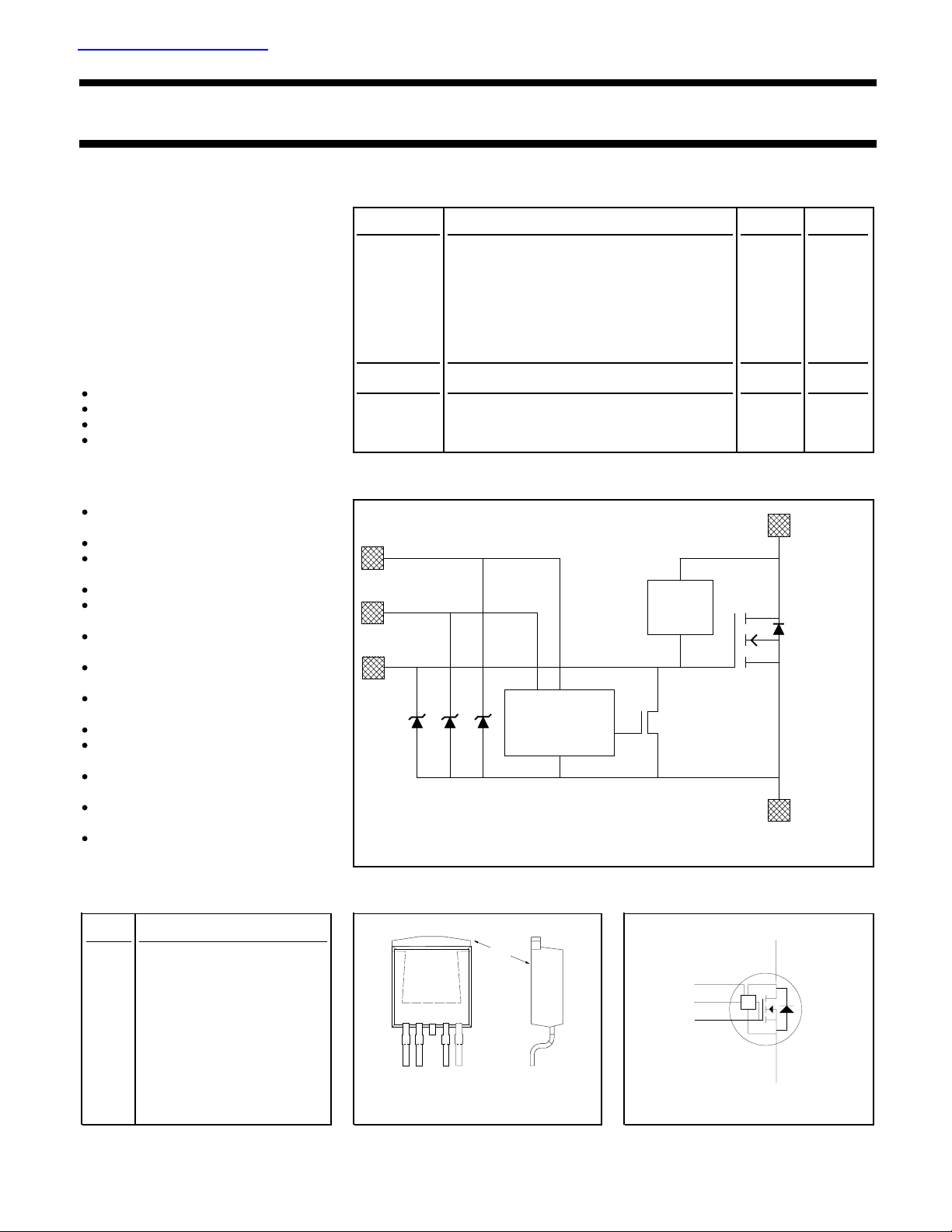
operation are possible Fig.1. Elements of the TOPFET.
PINNING - SOT426 PIN CONFIGURATION SYMBOL
PIN DESCRIPTION
1 input
2 flag
3 (connected to mb)
4 protection supply
5 source
mb drain
3
12 45
mb
Fig. 2. Fig. 3.
TOPFET
P
F
I
DRAIN
POWER
MOSFET
SOURCE
D
P
S
September 1996 1 Rev 1.000
Page 2

Philips Semiconductors Product specification
Logic level TOPFET BUK114-50L/S
SMD version of BUK104-50L/S
LIMITING VALUES
Limiting values in accordance with the Absolute Maximum Rating System (IEC 134)
SYMBOL PARAMETER CONDITIONS MIN. MAX. UNIT
V
V
V
V
I
D
I
D
I
DRM
P
T
T
T
DSS
IS
FS
PS
tot
stg
j
sold
Voltages
Continuous off-state drain source VIS = 0 V - 50 V
voltage
1
Continuous input voltage - 0 11 V
Continuous flag voltage - 0 11 V
Continuous supply voltage - 0 11 V
Currents VIS = - 7 5 V
Continuous drain current T
Continuous drain current T
Repetitive peak on-state drain current Tmb ≤ 25 ˚C - 60 54 A
25 ˚C - 15 13 A
mb ≤
100 ˚C - 9.5 8.5 A
mb ≤
Thermal
Total power dissipation Tmb = 25 ˚C - 40 W
Storage temperature - -55 150 ˚C
Junction temperature
2
continuous - 150 ˚C
Lead temperature during soldering - 250 ˚C
OVERLOAD PROTECTION LIMITING VALUES
With the protection supply An n-MOS transistor turns on For internal overload protection to
connected, TOPFET can protect between the input and source to remain latched while the control
itself from two types of overload - quickly discharge the power circuit is high, external series input
over temperature and short circuit MOSFET gate capacitance. resistance must be provided. Refer
load. to INPUT CHARACTERISTICS.
SYMBOL PARAMETER CONDITIONS MIN. MAX. UNIT
VIS =75 - V
V
PSP
Protection supply voltage
3
for valid protection
BUK114-50L 4.4 4 - V
BUK114-50S 5.4 5 - V
V
DDP(T)
V
DDP(P)
P
DSM
Over temperature protection VPS = V
Protected drain source supply voltage VIS = 10 V; RI ≥ 2 kΩ -50V
V
Short circuit load protection VPS = V
Protected drain source supply voltage4VIS = 10 V; RI ≥ 2 kΩ -25V
V
Instantaneous overload dissipation - 0.8 kW
PSN
= 5 V; RI ≥ 1 kΩ -50V
IS
; L ≤ 10 µH
PSN
= 5 V; RI ≥ 1 kΩ -45V
IS
ESD LIMITING VALUE
SYMBOL PARAMETER CONDITIONS MIN. MAX. UNIT
V
C
Electrostatic discharge capacitor Human body model; - 2 kV
voltage C = 250 pF; R = 1.5 kΩ
1 Prior to the onset of overvoltage clamping. For voltages above this value, safe operation is limited by the overvoltage clamping energy.
2 A higher Tj is allowed as an overload condition but at the threshold T
3 The minimum supply voltage required for correct operation of the overload protection circuits.
4 The device is able to self-protect against a short circuit load providing the drain-source supply voltage does not exceed V
For further information, refer to OVERLOAD PROTECTION CHARACTERISTICS.
the over temperature trip operates to protect the switch.
j(TO)
DDP(P)
maximum.
September 1996 2 Rev 1.000
Page 3

Philips Semiconductors Product specification
Logic level TOPFET BUK114-50L/S
SMD version of BUK104-50L/S
OVERVOLTAGE CLAMPING LIMITING VALUES
At a drain source voltage above 50 V the power MOSFET is actively turned on to clamp overvoltage transients.
SYMBOL PARAMETER CONDITIONS MIN. MAX. UNIT
I
DRRM
E
DSM
E
DRM
Repetitive peak clamping drain current RIS ≥ 100 Ω
Non-repetitive inductive turn-off IDM = 15 A; RIS ≥ 100 Ω - 200 mJ
energy
2
Repetitive inductive turn-off energy RIS ≥ 100 Ω; Tmb ≤ 95 ˚C; - 20 mJ
IDM = 4 A; VDD ≤ 20 V;
f = 250 Hz
I
DIRM
Repetitive peak drain to input current3RIS = 0 Ω; tp ≤ 1 ms - 50 mA
REVERSE DIODE LIMITING VALUE
SYMBOL PARAMETER CONDITIONS MIN. MAX. UNIT
I
S
Continuous forward current Tmb = 25 ˚C; - 15 A
VIS = VPS = VFS = 0 V
THERMAL CHARACTERISTIC
1
-15A
SYMBOL PARAMETER CONDITIONS MIN. TYP. MAX. UNIT
Thermal resistance
R
th j-mb
Junction to mounting base - - 2.5 3.1 K/W
STATIC CHARACTERISTICS
Tmb = 25 ˚C unless otherwise specified
SYMBOL PARAMETER CONDITIONS MIN. TYP. MAX. UNIT
V
(CL)DSR
V
(CL)DSR
I
DSS
I
DSR
I
DSR
R
DS(ON)
Drain-source clamping voltage RIS = 100 Ω; ID = 10 mA 50 - 65 V
Drain-source clamping voltage RIS = 100 Ω; IDM = 1 A; tp ≤ 300 µs; 50 - 70 V
δ ≤ 0.01
Zero input voltage drain current VDS = 12 V; VIS = 0 V - 0.5 10 µA
Drain source leakage current VDS = 50 V; RIS = 100 Ω;-120µA
Drain source leakage current VDS = 40 V; RIS = 100 Ω;
Tj = 125 ˚C - 10 100 µA
Drain-source on-state IDM = 7.5 A; VIS = 7 V - 75 100 mΩ
resistance tp ≤ 300 µs; δ ≤ 0.01 VIS = 5 V - 95 125 mΩ
1 The input pin must be connected to the source pin by a specified external resistance to allow the power MOSFET gate source voltage to
2 While the protection supply voltage is connected, during overvoltage clamping it is possible that the overload protection may operate at
3 Shorting the input to source with low resistance inhibits the internal overvoltage protection by preventing the power MOSFET gate source
become sufficiently positive for active clamping. Refer to INPUT CHARACTERISTICS.
energies close to the limiting value. Refer to OVERLOAD PROTECTION CHARACTERISTICS.
voltage becoming positive.
September 1996 3 Rev 1.000
Page 4

Philips Semiconductors Product specification
Logic level TOPFET BUK114-50L/S
SMD version of BUK104-50L/S
OVERLOAD PROTECTION CHARACTERISTICS
With adequate protection supply Provided there is adequate input Refer also to OVERLOAD
voltage TOPFET detects when one series resistance it switches off PROTECTION LIMITING VALUES
of the overload thresholds is and remains latched off until reset and INPUT CHARACTERISTICS.
exceeded. by the protection supply pin.
SYMBOL PARAMETER CONDITIONS MIN. TYP. MAX. UNIT
Short circuit load protection1VPS = V
RI ≥ 2 kΩ
E
t
d sc
DS(TO)
Overload threshold energy VDD = 13 V; VIS = 10 V - 150 - mJ
Response time VDD = 13 V; VIS = 10 V - 375 - µs
Over temperature protection VPS = V
T
j(TO)
Threshold junction temperature from ID ≥ 0.65 A
TRANSFER CHARACTERISTICS
Tmb = 25 ˚C
SYMBOL PARAMETER CONDITIONS MIN. TYP. MAX. UNIT
g
fs
I
D
Forward transconductance VDS = 10 V; IDM = 7.5 A tp ≤ 300 µs; 5 9 - S
δ ≤ 0.01
Drain current
4
VDS = 13 V; VIS = 5 V - 25 - A
2
; Tmb = 25 ˚C; L ≤ 10 µH;
PSN
; RI ≥ 2 kΩ
PSN
3
VIS = 10 V 40 - A
150 - - ˚C
PROTECTION SUPPLY CHARACTERISTICS
Tmb = 25 ˚C unless otherwise specified
SYMBOL PARAMETER CONDITIONS MIN. TYP. MAX. UNIT
Protection supply
IPS, Protection supply current normal operation or
I
PSL
protection latched
BUK114-50L VPS = 5 V - 0.2 0.35 mA
V
PSR
Protection reset voltage
5
BUK114-50S VPS = 10 V - 0.4 1.0 mA
1.5 2.5 3.5 V
Tj = 150 ˚C 1.0 - - V
V
(CL)PS
Protection clamp voltage IP = 1.35 mA 11 13 - V
REVERSE DIODE CHARACTERISTICS
Tmb = 25 ˚C
SYMBOL PARAMETER CONDITIONS MIN. TYP. MAX. UNIT
V
SDS
t
rr
1 The short circuit load protection is able to save the device providing the instantaneous on-state dissipation is less than the limiting value for
2 At the appropriate nominal protection supply voltage for each type. Refer to QUICK REFERENCE DATA.
3 The over temperature protection feature requires a minimum on-state drain source voltage for correct operation. The specified minimum I
4 During overload condition. Refer also to OVERLOAD PROTECTION LIMITING VALUES and CHARACTERISTICS.
5 The supply voltage below which the overload protection circuits will be reset.
6 The reverse diode of this type is not intended for applications requiring fast reverse recovery.
Forward voltage IS = 15 A; VIS = VPS = VFS = 0 V; - 1.0 1.5 V
tp = 300 µs
Reverse recovery time not applicable
P
, which is always the case when VDS is less than V
DSM
ensures this condition.
maximum.
DSP
6
----
D
September 1996 4 Rev 1.000
Page 5

Philips Semiconductors Product specification
Logic level TOPFET BUK114-50L/S
SMD version of BUK104-50L/S
INPUT CHARACTERISTICS
Tmb = 25 ˚C unless otherwise specified
SYMBOL PARAMETER CONDITIONS MIN. TYP. MAX. UNIT
Normal operation
V
I
IS
V
R
R
R
IS(TO)
(CL)IS
ISL
IS
I
Input threshold voltage VDS = 5 V; ID = 1 mA 1.0 1.5 2.0 V
Tmb = 150 ˚C 0.5 - - V
Input current VIS = 10 V - 10 100 nA
Input clamp voltage II = 1 mA 11 13 - V
Overload protection latched
Input resistance
1
VPS = 5 V II = 5 mA; - 55 - Ω
Tmb = 150 ˚C - 95 - Ω
VPS = 10 V II = 5 mA; - 35 - Ω
Tmb = 150 ˚C - 60 - Ω
Application information
External input resistances for (see figure 29)
internal overvoltage clamping2RI = ∞ Ω;V
internal overload protection
3
RIS = ∞ Ω;V
> 30 V 100 - - Ω
DS
= 5 V 1 - - kΩ
II
VII = 10 V 2 - - kΩ
SWITCHING CHARACTERISTICS
Tmb = 25 ˚C; RI = 50 Ω; RIS = 50 Ω (see figure 29); resistive load RL = 10 Ω. For waveforms see figure 28.
SYMBOL PARAMETER CONDITIONS MIN. TYP. MAX. UNIT
t
t
t
t
d on
r
d off
f
Turn-on delay time VDD = 15 V; VIS: 0 V ⇒ 10 V - 8 - ns
Rise time - 13 - ns
Turn-off delay time VDD = 15 V; VIS: 10 V ⇒ 0 V - 100 - ns
Fall time - 45 - ns
CAPACITANCES
Tmb = 25 ˚C; f = 1 MHz
SYMBOL PARAMETER CONDITIONS MIN. TYP. MAX. UNIT
C
iss
C
oss
C
rss
C
pso
C
fso
Input capacitance VDS = 25 V; VIS = 0 V - 415 600 pF
Output capacitance VDS = 25 V; VIS = 0 V - 275 400 pF
Reverse transfer capacitance VDS = 25 V; VIS = 0 V - 55 80 pF
Protection supply pin VPS = 10 V - 30 - pF
capacitance
Flag pin capacitance VFS = 10 V; VPS = 0 V - 20 - pF
1 The resistance of the internal transistor which discharges the power MOSFET gate capacitance when overload protection operates.
The external drive circuit should be such that the input voltage does not exceed V
operated. Refer also to figure for latched input characteristics.
2 Applications using a lower value for RIS would require external overvoltage protection.
3 For applications requiring a lower value for RI, an external overload protection strategy is possible using the flag pin to ‘tell’ the control circuit to
switch off the input.
minimum when the overload protection has
IS(TO)
September 1996 5 Rev 1.000
Page 6

Philips Semiconductors Product specification
Logic level TOPFET BUK114-50L/S
SMD version of BUK104-50L/S
FLAG DESCRIPTION TRUTH TABLE
The flag pin provides a means to CONDITION DESCRIPTION FLAG
detect the presence of the
protection supply and indicate the NORMAL Normal operation and adequate LOGIC LOW
state of the overload detectors. protection supply voltage
The flag is the open drain of an
n-MOS transistor and requires an OVER TEMP. Over temperature detected LOGIC HIGH
external pull-up resistor1. It is
suitable for both 5 V and 10 V logic.
Flag may be used to implement an SHORT CIRCUIT Overload condition detected LOGIC HIGH
external protection strategy2 for
applications which require low input
drive impedance. SUPPLY FAULT Inadequate protection supply LOGIC HIGH
voltage
FLAG CHARACTERISTICS
Tmb = 25 ˚C unless otherwise stated
SYMBOL PARAMETER CONDITIONS MIN. TYP. MAX. UNIT
Flag ‘low’ normal operation
V
I
I
V
V
R
FSS
FS
FS
PSF
(CL)FS
F
Flag voltage IF = 1.6 mA - 0.15 0.4 V
Flag saturation current VFS = 10 V - 15 - mA
Flag ‘high’ overload or fault
Flag leakage current VFS = 10 V - - 10 µA
Protection supply threshold VFF = 5 V; RF = 3 kΩ;
voltage BUK114-50L 2.5 3.3 4 V
BUK114-50S 3.3 4.2 5 V
Flag clamping voltage IF = 1 mA; VPS = 0 V 11 13 - V
Application information
Suitable external pull-up VFF =5 V 1 10 50 kΩ
resistance VFF =10 V 2 20 100 kΩ
1 Even if the flag pin is not used, it is recommended that it is connected to the protection supply via a pull-up resistor. It should not be left
2 Low pass filtering of the flag signal may be advisable to prevent false tripping.
floating.
September 1996 6 Rev 1.000
Page 7
Philips Semiconductors Product specification
Logic level TOPFET BUK114-50L/S
SMD version of BUK104-50L/S
PD%
120
110
100
90
80
70
60
50
40
30
20
10
0
0 20 40 60 80 100 120 140
Normalised Power Derating
Tmb / C
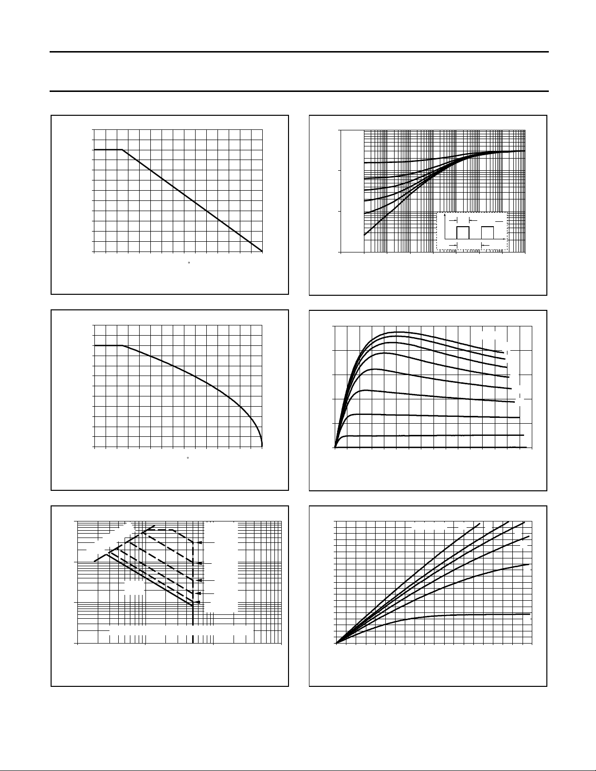
Fig.4. Normalised limiting power dissipation.
PD% = 100⋅PD/PD(25 ˚C) = f(Tmb)
ID%
120
110
100
90
80
70
60
50
40
30
20
10
0
0 20 40 60 80 100 120 140
Normalised Current Derating
Tmb / C
Fig.5. Normalised continuous drain current.
ID% = 100⋅ID/ID(25 ˚C) = f(Tmb); conditions: VIS = 5 V
p
t
T
BUK114-50L/S
t
p
D =
T
t
Zth / (K/W)
10
D =
0.5
1
0.2
0.1
0.05
0.1
0.02
0
0.01
1E-07 1E-05 1E-03 1E-01 1E+01
t / s
P
D
Fig.7. Transient thermal impedance.
Zth
= f(t); parameter D = tp/T
j-mb
ID / A
50
40
30
20
10
0
0 4 8 12 16 20 24 28 32
VDS / V
BUK114-50L/S
VIS / V =
10
9
8
7
6
Fig.8. Typical output characteristics, Tj = 25 ˚C.
ID = f(VDS); parameter VIS; tp = 250 µs & tp < t
5
4
3
2
d sc
tp =
10 us
100 us
1 ms
10 ms
100 ms
BUK114-50L/S
p
10 7VIS / V =
BUK114-50L/S
6
5
4
3
ID / A
20
15
10
5
0
0 1 2
VDS / V
Fig.9. Typical on-state characteristics, Tj = 25 ˚C.
ID = f(VDS); parameter VIS; tp = 250 µs
ID & IDM / A
100
RDS(ON) = VDS/ID
10
DC
1
Overload protection characteristics not shown
0.1
1 100
10
VDS / V
Fig.6. Safe operating area. Tmb = 25 ˚C
ID & IDM = f(VDS); IDM single pulse; parameter t
September 1996 7 Rev 1.000
Page 8
Philips Semiconductors Product specification
Logic level TOPFET BUK114-50L/S
SMD version of BUK104-50L/S
RDS(ON) / mOhm
150
100
50
0
0 2 4 6 8 10 12 14 16 18 20
4VIS / V =
ID / A
BUK114-50L/S
5
6
7
10
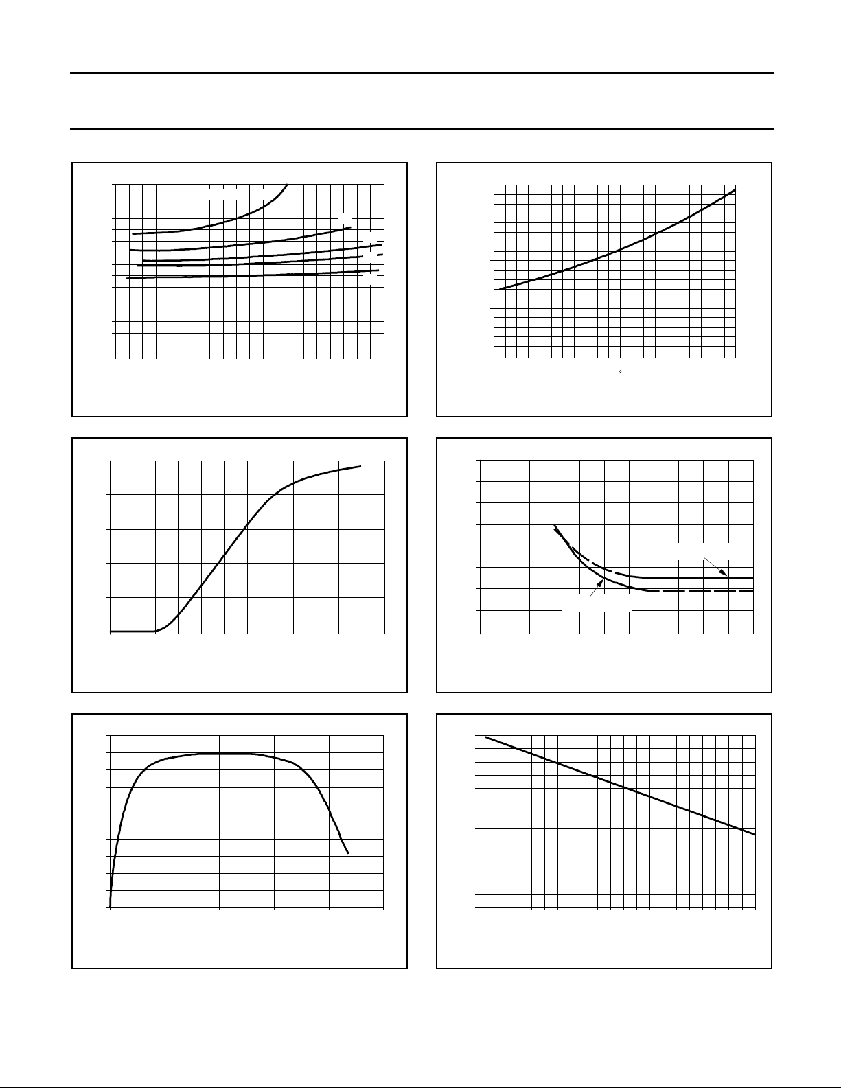
Fig.10. Typical on-state resistance, Tj = 25 ˚C.
R
= f(ID); parameter VIS; tp = 250 µs
DS(ON)
ID / A
50
40
30
20
10
0
0 2 4 6 8 10 12
VIS / V
BUK114-50L/S
Fig.11. Typical transfer characteristics, Tj = 25 ˚C.
ID = f(VIS) ; conditions: VDS = 10 V; tp = 250 µs
a
1.5
1.0
0.5
0
-60 -40 -20 0 20 40 60 80 100 120 140
Normalised RDS(ON) = f(Tj)
Tj / C
Fig.13. Normalised drain-source on-state resistance.
a = R
DS(ON)/RDS(ON)
Tj(TO) / C
230
220
210
200
190
180
170
160
150
0 2 4 6 8 10
25 ˚C = f(Tj); ID = 7.5 A; VIS ≥ 5 V
BUK114-50L/S
BUK114-50S
BUK114-50L
VPS / V
Fig.14. Typical over temperature protection threshold
T
= f(VPS); conditions: VDS > 0.1 V
j(TO)
gfs / S
10
9
8
7
6
5
4
3
2
1
0
0 20 40
10 30 50
ID / A
BUK114-50L/S
Fig.12. Typical transconductance, Tj = 25 ˚C.
gfs = f(ID); conditions: VDS = 10 V; tp = 250 µs
PDSM%
120
100
80
60
40
20
0
-60 -40 -20 0 20 40 60 80 100 120 140
Tmb / C
Fig.15. Normalised limiting overload dissipation.
P
% =100⋅P
DSM
DSM/PDSM
(25 ˚C) = f(Tmb)
September 1996 8 Rev 1.000
Page 9
Philips Semiconductors Product specification
Logic level TOPFET BUK114-50L/S
SMD version of BUK104-50L/S
VDDP(P) / V
50
40
BUK114-50L/S
max
30
20
10
0
0 2 4 6 8 10
VIS / V
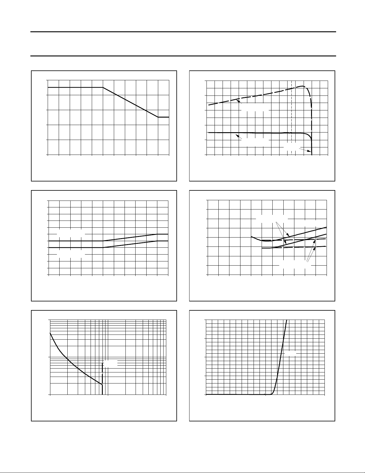
Fig.16. Maximum drain source supply voltage for
SC load protection. V
VPSP / V
10
8
6
4
2
BUK114-50S
BUK114-50L
= f(VIS); Tmb ≤ 150 ˚C
DDP(P)
min
BUK114-50L/S
Energy & Time
0.5
0.4
0.3
0.2
0.1
0
-60 -20 20 60 100 140 180 220
Time / ms
Energy / J
Tmb / C
BUK114-50L/S
Tj(TO)
Fig.19. Typical overload protection characteristics.
Conditions: VDD = 13 V; VPS = V
ESC(TO) / J
0.4
0.3
0.2
0.1
BUK114-50L
, VIS = 7 V; SC load
PSN
BUK114-50L/S
VIS / V =
BUK114-50S
5
10
5
10
0
0 2 4 6 8 10
VIS / V
Fig.17. Minimum protection supply voltage
for SC load protection. V
TIME / ms
10
1
0.1
0.1 1 10
POWER / kW
= f(VIS); Tmb ≥ 25 ˚C
PSP
BUK114-50L/S
PDSM
Fig.18. Typical overload protection characteristics.
t
= f(PDS); conditions: VPS ≥ V
d sc
; VIS ≥ 5 V
PSP
0
0 2 4 6 8 10
VPS / V
Fig.20. Typical overload protection energy, Tj = 25 ˚C
E
= f(VPS); conditions: VDS = 13 V, parameter V
SC(TO)
ID / A
20
15
10
5
0
50 60 70
VDS / V
BUK114-50L/S
typ.
IS
Fig.21. Typical clamping characteristics, 25 ˚C.
ID = f(VDS); conditions: RIS = 100 Ω; tp ≤ 50 µs
September 1996 9 Rev 1.000
Page 10
Philips Semiconductors Product specification
Logic level TOPFET BUK114-50L/S
SMD version of BUK104-50L/S
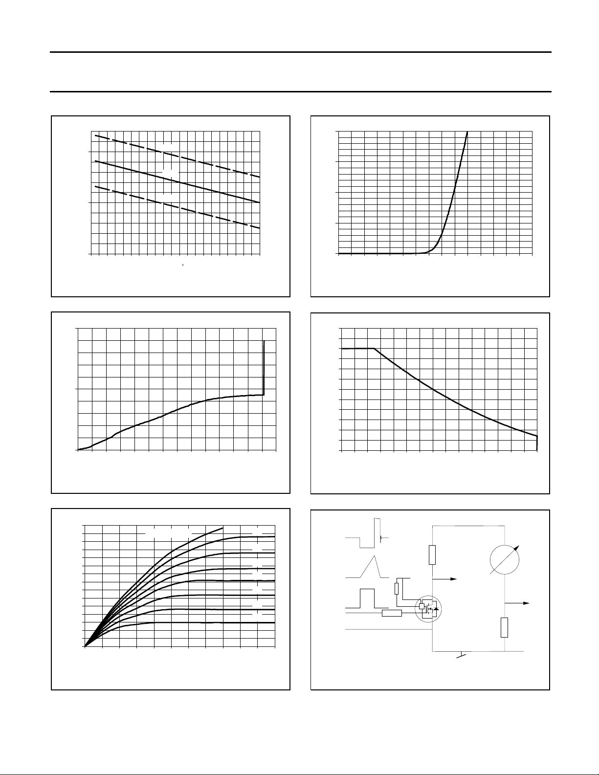
VIS(TO) / V
2
1
0
-60 -40 -20 0 20 40 60 80 100 120 140
max.
typ.
min.
Tj / C
Fig.22. Input threshold voltage.
V
= f(Tj); conditions: ID = 1 mA; VDS = 5 V
IS(TO)
IPS / mA
1.0
0.5
0
0 2 4 6 8 10 12 14
VPS / V
BUK114-50L/S
Fig.23. Typical DC protection supply characteristics.
IPS = f(VPS); normal or overload operation; Tj = 25 ˚C
20
15
10
IS / A
5
0
0
0.5
VSD / V
1
BUK114-50L/S
1.5
Fig.25. Typical reverse diode current, Tj = 25 ˚C.
IS = f(V
EDSM%
120
110
100
90
80
70
60
50
40
30
20
10
0
0 20 40 60 80 100 120 140
); conditions: VIS = 0 V; tp = 250 µs
SDS
Tmb / C
Fig.26. Normalised limiting clamping energy.
E
% = f(Tmb); conditions: ID = 15 A
DSM
IISL / mA
150
100
50
0
0 2 4 6 8 10
VPS / V = 11
VIS / V
Fig.24. Typical latched input characteristics, 25 ˚C.
I
= f(VIS); after overload protection latched
ISL
BUK114-50L/S
10
9
8
7
6
5
4
VDS
0
ID
0
VIS
0
RI = RIS
Fig.27. Clamping energy test circuit, RIS = 100 Ω.
E
DSM
V(CL)DSR
VDD
RF
= 0.5 ⋅LI
VDD
+
L
P
(CL)DSR
D
TOPFET
D.U.T.
S
/(V
VDS
R 01
shunt
(CL)DSR−VDD
-
-ID/100
)
VPS
+
P
F
I
2
⋅ V
D
September 1996 10 Rev 1.000
Page 11
Philips Semiconductors Product specification
Logic level TOPFET BUK114-50L/S
SMD version of BUK104-50L/S
VIS / V & VDS / V
15
VDS
VIS
10
5
0
0 0.5 1
time / us
BUK114-50L/S
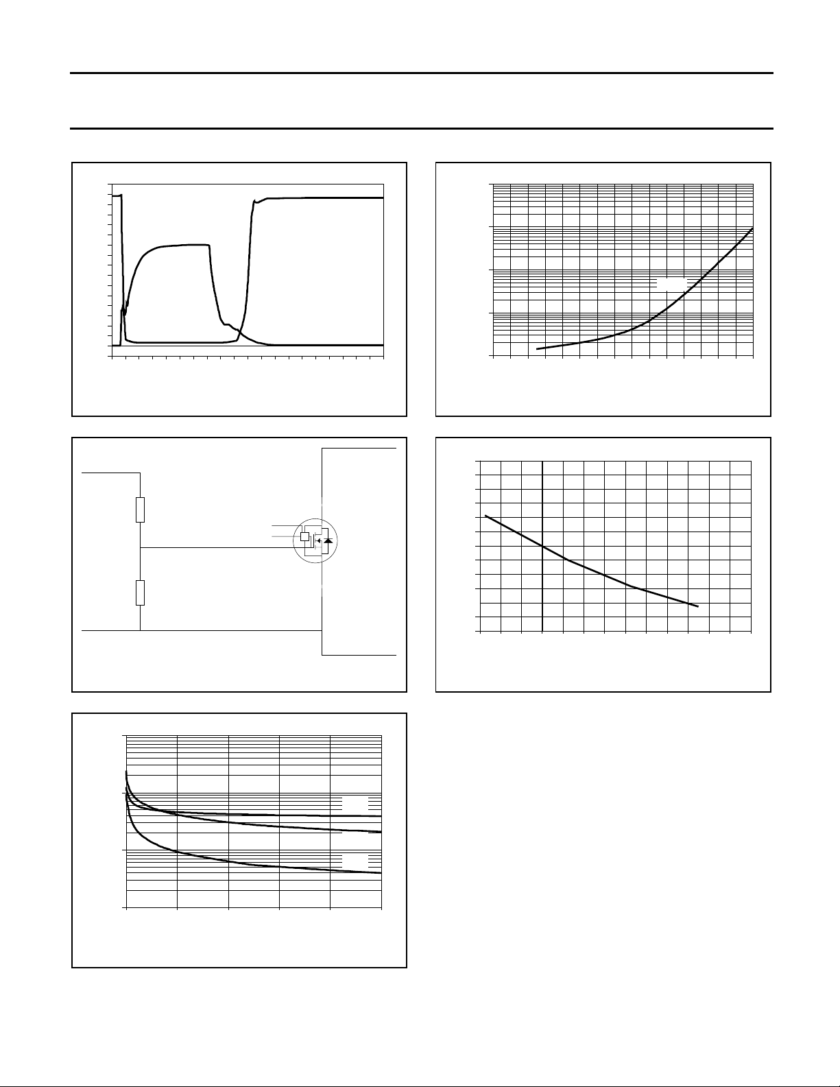
Fig.28. Typical resistive load switching waveforms
RI = RIS = 50 Ω; RL = 10 Ω; VDD = 15 V; Tj = 25 ˚C
VII
RI
RIS
VIS
TOPFET
P
F
I
D
P
S
Idsr
1 mA
100 uA
10 uA
typ.
1 uA
100 nA
0 20 40 60 80 100 120 140
Tj / C
Fig.31. Typical off-state leakage current.
I
= f(Tj); Conditions: VDS = 40 V; RIS = 100 Ω.
DSR
Ips normalised to 25 C
1.5
1
Fig.29. External input resistances RI and RIS,
generator voltage VII and input voltage VIS.
Capacitance / pF
10000
1000
100
10
0 20 40
VDS / V
Fig.30. Typical capacitances, C
C = f(VDS); conditions: VIS = 0 V; f = 1 MHz
BUK114-50L/S
, C
iss
oss
Ciss
Coss
Crss
, C
rss
0.5
-60 -20 20 60 100 140 180
Tj / C
Fig.32. Normalised protection supply current.
IPS/IPS25 ˚C = f(Tj); VPS = V
503010
PSN
.
September 1996 11 Rev 1.000
Page 12
Philips Semiconductors Product specification
Logic level TOPFET BUK114-50L/S
SMD version of BUK104-50L/S
MECHANICAL DATA
Dimensions in mm
Net Mass: 1.5 g
MOUNTING INSTRUCTIONS
Dimensions in mm
10.3 MAX
1.4 MAX
11 MAX
15.4
2.5
0.85 MAX
(x4)
3.4
1.7
1.7
3.4
0.5
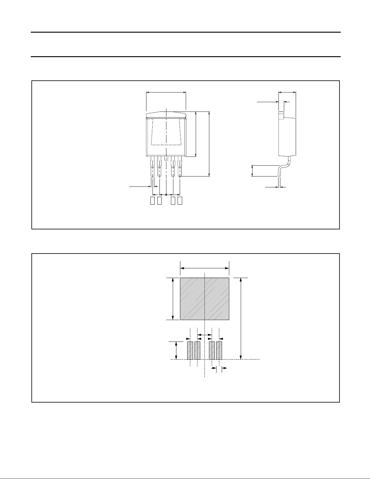
Fig.33. SOT426
mounting base connected to centre pin (cropped short)
11.5
4.5 MAX
9.0
17.5
3.4
1.7
3.8
1.7
1.3 (x4)
Fig.34. SOT426
soldering pattern for surface mounting.
September 1996 12 Rev 1.000
Page 13

Philips Semiconductors Product specification
Logic level TOPFET BUK114-50L/S
SMD version of BUK104-50L/S
DEFINITIONS
Data sheet status
Objective specification This data sheet contains target or goal specifications for product development.
Preliminary specification This data sheet contains preliminary data; supplementary data may be published later.
Product specification This data sheet contains final product specifications.
Limiting values
Limiting values are given in accordance with the Absolute Maximum Rating System (IEC 134). Stress above one
or more of the limiting values may cause permanent damage to the device. These are stress ratings only and
operation of the device at these or at any other conditions above those given in the Characteristics sections of
this specification is not implied. Exposure to limiting values for extended periods may affect device reliability.
Application information
Where application information is given, it is advisory and does not form part of the specification.
Philips Electronics N.V. 1996
All rights are reserved. Reproduction in whole or in part is prohibited without the prior written consent of the
copyright owner.
The information presented in this document does not form part of any quotation or contract, it is believed to be
accurate and reliable and may be changed without notice. No liability will be accepted by the publisher for any
consequence of its use. Publication thereof does not convey nor imply any license under patent or other
industrial or intellectual property rights.
LIFE SUPPORT APPLICATIONS
These products are not designed for use in life support appliances, devices or systems where malfunction of these
products can be reasonably expected to result in personal injury. Philips customers using or selling these products
for use in such applications do so at their own risk and agree to fully indemnify Philips for any damages resulting
from such improper use or sale.
September 1996 13 Rev 1.000
 Loading...