

Page 1
HIGH VOLTAGE FAST-SWITCHING
■ STMicroelectronicsPREFERRED
SALESTYPE
■ HIGH VOLTAGECAPABILITY
■ U.L.RECOGNISEDISOWATT218 PACKAGE
(U.L. FILE # E81734 (N)).
BUH315
NPN POWER TRANSISTOR
APPLICATIONS:
■ HORIZONTAL DEFLECTIONFOR COLOUR
TV
■ SWITCHMODEPOWERSUPPLIES
DESCRIPTION
The BUH315 is manufactured using Multiepitaxial
Mesa technology for cost-effective high
performanceand usesa Hollow Emitterstructure
to enhanceswitchingspeeds.
The BUH series is designed for use in horizontal
deflectioncircuits in televisionsand monitors.
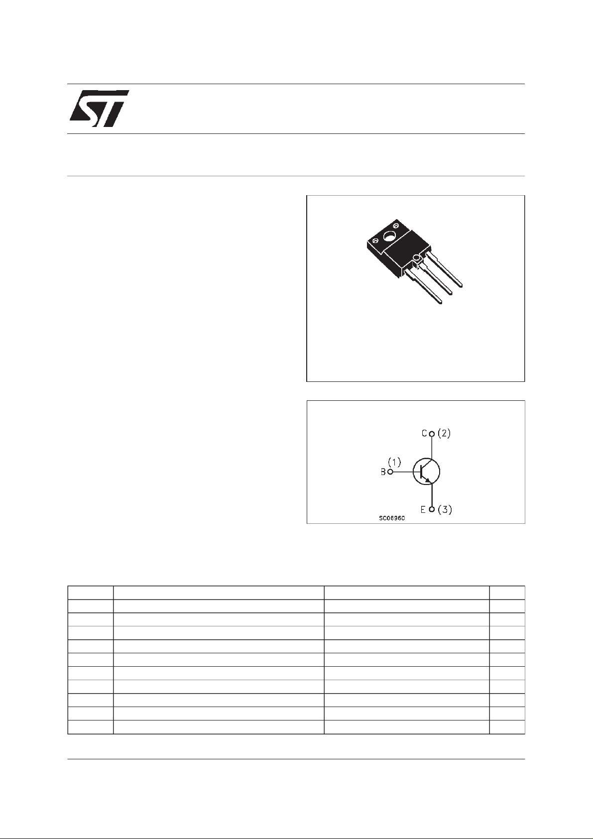
3
2
1
ISOWATT218
INTERNAL SCHEMATIC DIAGRAM
ABSOLUTE MAXIMUM RATINGS
Symbol Parameter Value Unit
V
V
V
I
I
P
T
November 1999
Collect or-Base Vol tage (IE= 0 ) 1500 V
CBO
Collect or-Emitter Volt age ( IB= 0 ) 700 V
CEO
Emitter-Base Vol tage (IC=0) 10 V
EBO
Collect or Current 6 A
I
C
Collect or Peak Cu r rent (tp<5ms) 12 A
CM
Base Current 3 A
I
B
Base P eak Current (tp<5ms) 5 A
BM
Tot al Dissipation at Tc=25oC44W
tot
Storage Temperature -65 to 150
stg
Max. Ope r ating Jun c tion Te m pe r ature 150
T
j
o
C
o
C
1/7
Page 2
BUH315
THERMAL DATA
R
thj-case
Ther mal Resist ance Junctio n-c a se Max 2.8
o
C/W
ELECTRICAL CHARACTERISTICS (T
=25oC unlessotherwisespecified)
case
Symbol Parameter Test Cond itions Min. Typ. Max. Un it
I
CES
I
EBO
V
CEO(sus)
Collec t or Cut -off
Current (V
BE
=0)
Emitt er Cut -of f Current
=0)
(I
C
∗ Co llector-Emit t er
V
= 1500 V 200 µA
CE
V
=5V 100 µA
EB
I
= 10 0 m A 700 V
C
Sust aining Voltage
=0)
(I
B
V
V
CE(sat)
EBO
Emitter-Base Voltage
(I
=0)
C
∗ Collec t or -Emit t er
=10mA 10 V
I
E
IC=3A IB=0.75A 1.5 V
Saturation Voltage
∗ Base-Emi tter
V
BE(sat)
IC=3A IB=0.75A 1.3 V
Saturation Voltage
∗ DC Current Gain IC=3A VCE=5V
h
FE
t
t
t
t
RESI STIVE LOAD
Storage Ti me
s
Fall Time
f
INDUCTIVE LOAD
Storage Ti me
s
Fall Time
f
=3A VCE=5V Tj=100oC
I
C
VCC=400V IC=3A
=0.75A IB2= 1.5 A 1.6
I
B1
IC= 3 A f = 15625 Hz
I
=0.75A IB2=-1.5A
B1
V
ceflyback
=1050sin
6
3.5
110
3.5
π
6
tV
10
5
340
12
2.4
200
µs
ns
µs
ns
INDUCTIVE LOAD
s
t
f
Storage Ti me
Fall Time
t
∗
Pulsed: Pulse duration = 300 µs, duty cycle 1.5 %
IC= 3 A f = 31250 Hz
=0.75A IB2=-1.5A
I
B1
π
V
ceflyback
=1200sin
6
10
5
tV
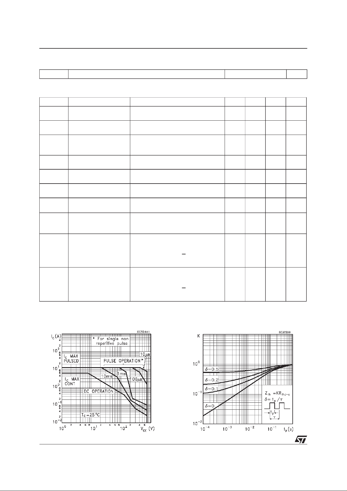
Safe Operating Area Thermal Impedance
2/7
3.5
270
µs
ns
Page 3
BUH315
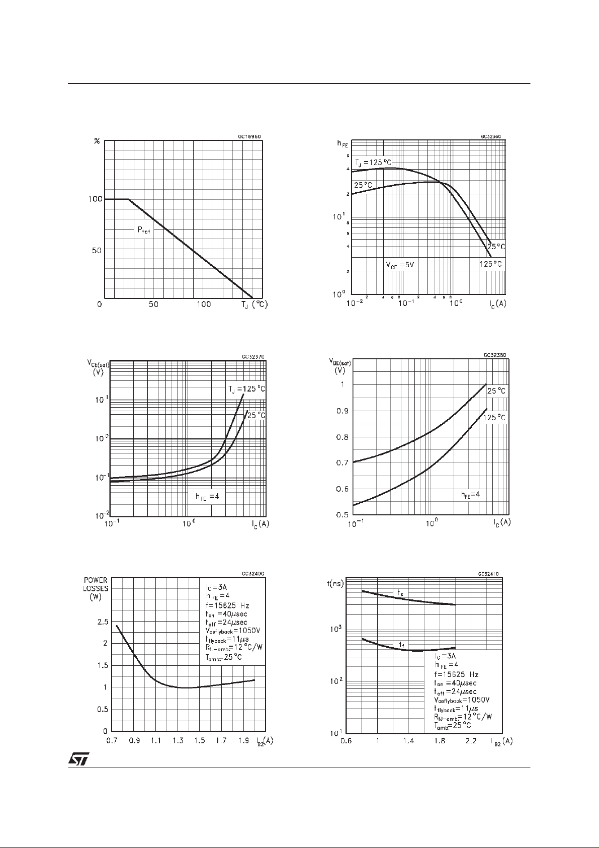
Derating Curve
CollectorEmitterSaturationVoltage
DC Current Gain
BaseEmitterSaturation Voltage
PowerLosses at 16 KHz
SwitchingTime InductiveLoad at 16KHz
(see figure 2)
3/7
Page 4

BUH315
PowerLosses at 32 KHz SwitchingTime InductiveLoad at 32KHz
(see figure 2)
ReverseBiasedSOA
BASEDRIVE INFORMATION
In order to saturate the power switch and reduce
conduction losses, adequate direct base current
I
has to be provided for the lowest gain hFEat
B1
o
100
C (line scan phase). On the other hand,
negative base current I
must be provided to
B2
turn off the power transistor (retrace phase).
Most of the dissipation, in the deflection
application, occurs at switch-off. Therefore it is
essential to determine the value of I
minimizes power losses, fall time t
consequently,T
defined to give total power losses, t
function of I
. A new set of curves have been
j
s
at both 16 KHz and 32 KHz
B2
which
B2
and,
f
and tfas a
scanning frequencies for choosing the optimum
negative drive. The test circuit is illustrated in
4/7
figure 1.
Inductance L
negative base current I
serves to control the slope of the
1
to recombine the
B2
excess carrier in the collector when base current
is still present, this would avoid any tailing
phenomenonin the collectorcurrent.
The values of L and C are calculated from the
followingequations:
1
L(I
2
Where IC= operating collector current, V
C
)2=
1
2
C(V
CEfly
2
)
ω=2πf=
1
√
L
C
CEfly
flyback voltage, f= frequency of oscillation during
retrace.
=
Page 5

Figure1: Inductive Load Switching TestCircuits.
Figure2: SwitchingWaveformsin a Deflection Circuit
BUH315
5/7
Page 6

BUH315
ISOWATT218MECHANICAL DATA
DIM.
A 5.35 5.65 0.211 0.222
C 3.30 3.80 0.130 0.150
D 2.90 3.10 0.114 0.122
D1 1.88 2.08 0.074 0.082
E 0.75 0.95 0.030 0.037
F 1.05 1.25 0.041 0.049
F2 1.50 1.70 0.059 0.067
F3 1.90 2.10 0.075 0.083
G 10.80 11.20 0.425 0.441
H 15.80 16.20 0.622 0.638
L 9 0.354
L1 20.80 21.20 0.819 0.835
L2 19.10 19.90 0.752 0.783
L3 22.80 23.60 0.898 0.929
L4 40.50 42.50 1.594 1.673
L5 4.85 5.25 0.191 0.207
L6 20.25 20.75 0.797 0.817
N 2.1 2.3 0.083 0.091
R 4.6 0.181
DIA 3.5 3.7 0.138 0.146
MIN. TYP. MAX. MIN. TYP. MAX.
mm inch
- Weight: 4.9g (typ.)
- MaximumTorque(applied to mounting flange) Recommended: 0.8 Nm; Maximum:1 Nm
- Theside of thedissipatormust be flat within 80 µm
6/7
P025C/A
Page 7

BUH315
Information furnished is believed to beaccurate and reliable. However, STMicroelectronics assumes noresponsibility for the consequences
of use of such information nor for any infringement of patents or other rights of third parties which may result from its use. No license is
granted by implication or otherwise under any patent or patent rights of STMicroelectronics. Specification mentioned in this publication are
subject to change without notice. This publication supersedes and replaces all information previously supplied. STMicroelectronics products
are not authorized for use as critical components in life support devices or systems without express written approval of STMicroelectronics.
The ST logo is a trademark of STMicroelectronics
1999 STMicroelectronics – Printed in Italy – AllRights Reserved
STMicroelectronicsGROUP OF COMPANIES
Australia - Brazil - China - Finland - France - Germany - Hong Kong - India - Italy - Japan - Malaysia - Malta - Morocco -
Singapore- Spain - Sweden - Switzerland -United Kingdom - U.S.A.
http://www.st.com
.
7/7
 Loading...