

Page 1
HIGH VOLTAGE FAST-SWITCHING
■ STMicroelectronicsPREFERRED
SALESTYPE
■ HIGH VOLTAGECAPABILITY
■ VERYHIGH SWITCHINGSPEED
APPLICATIONS:
■ HORIZONTAL DEFLECTIONFOR COLOUR
TV AND MONITORS
DESCRIPTION
The BUH1215 is manufactured using
Multiepitaxial Mesa technology for cost-effective
high performance and uses a Hollow Emitter
structureto enhance switching speeds.
The BUH series is designed for use in horizontal
deflectioncircuits in televisionsand monitors.
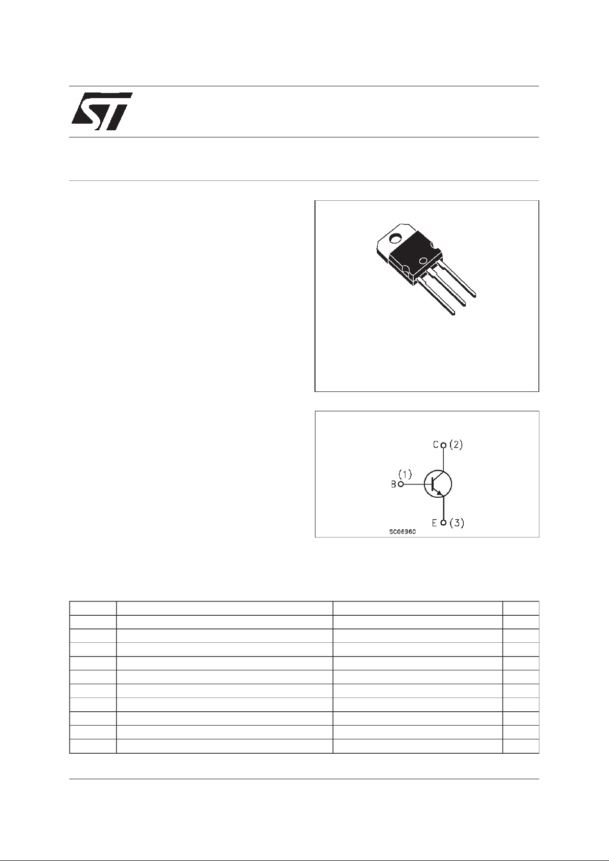
BUH1215
NPN POWER TRANSISTOR
3
2
1
TO-218
INTERNAL SCHEMATIC DIAGRAM
ABSOLUTE MAXIMUM RATINGS
Symbol Parameter Value Unit
V
V
V
I
I
P
T
Collect or-Base Vol t age ( IE= 0) 1500 V
CBO
Collect or-Emitte r Volt age ( IB= 0) 700 V
CEO
Emitter-Base Vol tage (IC=0) 10 V
EBO
Collect or Current 16 A
I
C
Collect or Peak Cu rr ent (tp<5ms) 22 A
CM
Base Current 9 A
I
B
Base P eak Cu rrent (tp<5ms) 12 A
BM
Tot al Dissipa t ion at Tc=25oC 200 W
tot
Storage Temperature -65 to 150
stg
Max. Ope r ating Jun c t io n T empe rature 150
T
j
o
C
o
C
January 1999
1/7
Page 2
BUH1215
THERMAL DATA
R
thj-case
Ther mal Resist ance Junctio n- case Max 0.63
o
C/W
ELECTRICAL CHARACTERISTICS (T
=25oC unlessotherwisespecified)
case
Symbol Parameter Test Cond itions Min. Typ. Max. Unit
I
CES
I
EBO
V
CEO(sus)
Collec t or Cut -off
Current (V
BE
=0)
Emitt er Cut -of f Cu rrent
=0)
(I
C
Collec t or -Emitter
V
= 1500 V
CE
= 1500 V Tj=125oC
V
CE
V
=5V 100 µA
EB
0.2
2
IC= 100 m A 700 V
Sust aining Volt age
V
EBO
Emitter-Base Voltage
(I
∗ Collec t or -Emitter
V
CE(sat)
C
=0)
I
=10mA 10 V
E
IC=12A IB= 2.4 A 1.5 V
Saturation Voltage
∗ Base-Emitter
V
BE(sat )
IC=12A IB= 2.4 A 1.5 V
Saturation Voltage
∗ DC C ur rent Ga in IC=12A VCE=5V
h
FE
t
t
t
t
RESI STIVE LOAD
Storage Ti me
s
Fall Time
f
INDUCTIVE LO AD
Storage Ti me
s
Fall Time
f
=12A VCE=5V Tj=100oC
I
C
VCC=400V IC=12A
I
=2A IB2=-6A 1.5
B1
IC= 12 A f = 31250 Hz
I
=2A IB2=-1.5A
B1
V
ceflyback
=1050sin
7
5
π
6
tV
10
5
10 14
110
4
220
mA
mA
µs
ns
µs
ns
INDUCTIVE LO AD
s
t
f
Storage Ti me
Fall Time
t
∗
Pulsed: Pulse duration = 300 µs, duty cycle 1.5 %
IC=6A f=64KHz
=1A V
I
B1
V
ceflyback
=1200sin
BE(of f)
=-2A
π
10
5
6
tV
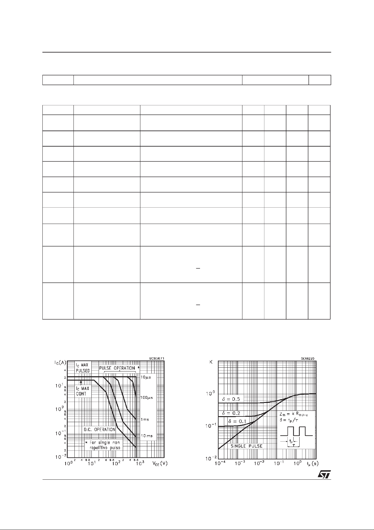
Safe Operating Area ThermalImpedance
3.5
180
µs
ns
2/7
Page 3
BUH1215
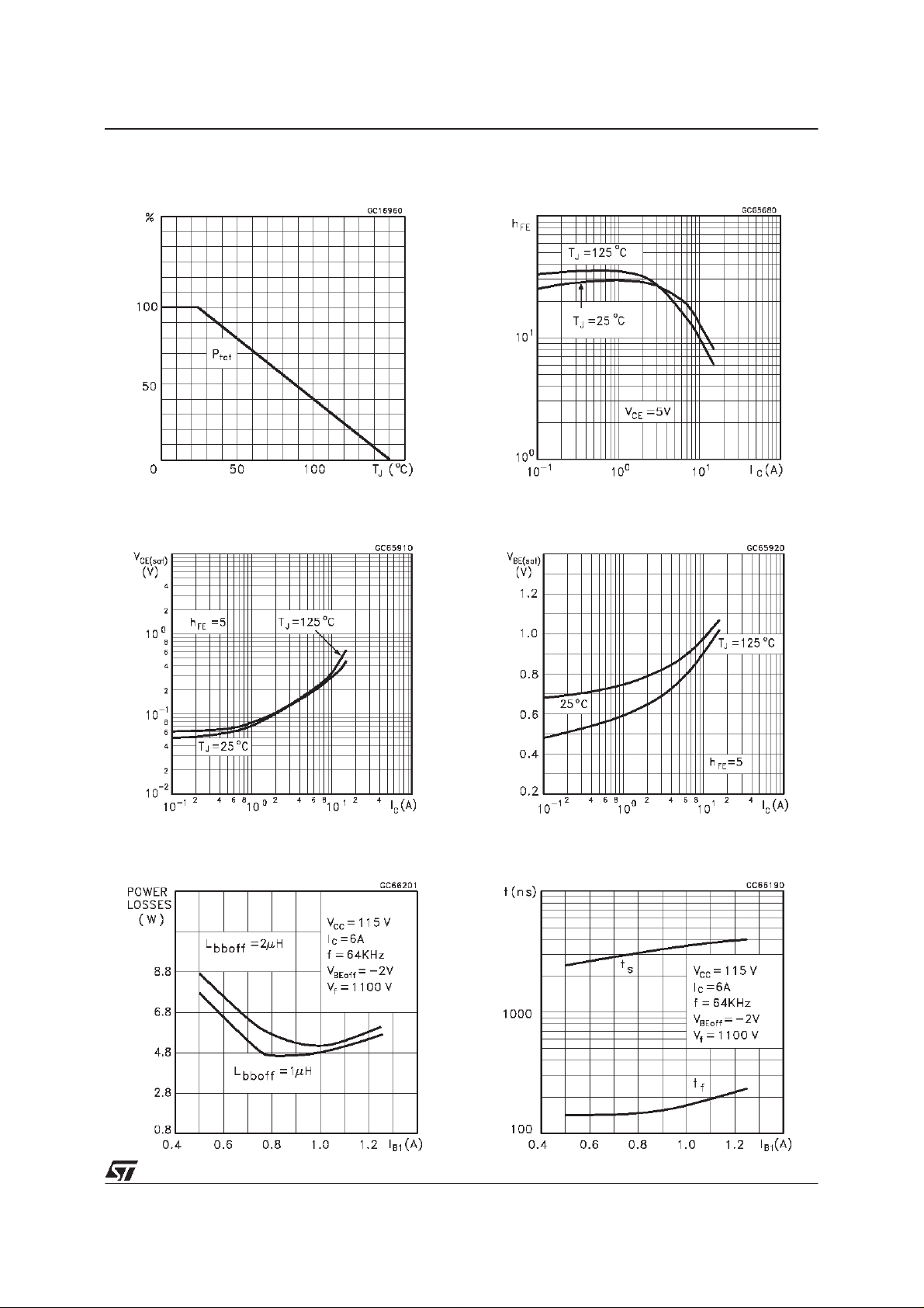
Derating Curve
CollectorEmitterSaturationVoltage
DC Current Gain
BaseEmitterSaturation Voltage
PowerLosses at 64 KHz
SwitchingTime InductiveLoad at 64 KHz
(see figure 2)
3/7
Page 4

BUH1215
ReverseBiasedSOA
BASEDRIVE INFORMATION
In order to saturate the power switch and reduce
conduction losses, adequate direct base current
I
has to be provided for the lowest gain hFEat
B1
o
C (line scan phase). On the other hand,
100
negative base current I
must be provided the
B2
transistorto turn off (retrace phase).
Most of the dissipation, especially in the
deflectionapplication, occurs at switch-off so it is
essential to determine the value of I
minimizes power losses, fall time t
consequently,T
defined to give total power losses, t
functionof I
. A new set of curves have been
j
s
at 64 KHz scanning frequenciesfor
B1
which
B2
and,
f
and tfas a
choosing the optimum negative drive. The test
circuitis illustratedin figure 1.
The values of L and C are calculated from the
followingequations:
C
)2=
1
2
1
L
√
C(V
C
CEfly
2
)
CEfly
1
L(I
2
ω=2πf=
Where IC= operating collector current, V
flyback voltage, f= frequency of oscillation during
retrace.
=
4/7
Page 5

Figure1: Inductive Load Switching TestCircuits.
Figure2: SwitchingWaveformsin aDeflection Circuit
BUH1215
5/7
Page 6

BUH1215
TO-218 (SOT-93) MECHANICAL DATA
DIM.
MIN. TYP. MAX. MIN. TYP. MAX.
A 4.7 4.9 0.185 0.193
C 1.17 1.37 0.046 0.054
D 2.5 0.098
E 0.5 0.78 0.019 0.030
F 1.1 1.3 0.043 0.051
G 10.8 11.1 0.425 0.437
H 14.7 15.2 0.578 0.598
L2 – 16.2 – 0.637
L3 18 0.708
L5 3.95 4.15 0.155 0.163
L6 31 1.220
R – 12.2 – 0.480
Ø 4 4.1 0.157 0.161
mm inch
E
A
C
L5
D
L6
L3
L2
H
G
¯
F
R
123
P025A
6/7
Page 7

BUH1215
Information furnished is believed to beaccurate and reliable. However, STMicroelectronics assumes noresponsibility for the consequences
of use of such information nor for any infringement of patents or other rights of third parties which may result from its use. No license is
granted by implication or otherwise under any patent or patent rights of STMicroelectronics. Specification mentioned in this publication are
subject to change without notice. This publication supersedes and replaces all information previously supplied. STMicroelectronics products
are not authorized for use as critical components in life support devices or systems without express written approval of STMicroelectronics.
The ST logo is a trademark of STMicroelectronics
1999 STMicroelectronics – Printed in Italy – All Rights Reserved
STMicroelectronicsGROUP OF COMPANIES
Australia - Brazil - Canada - China - France - Germany - Italy -Japan - Korea - Malaysia - Malta - Mexico - Morocco - The Netherlands -
Singapore - Spain - Sweden - Switzerland - Taiwan - Thailand - UnitedKingdom - U.S.A.
http://www.st.com
.
7/7
 Loading...