

Page 1

BUH1015
HIGH VOLTAGE FAST-SWITCHING
■ STMicroelectronics PREFERRED
SALESTYPES
■ HIGH VOLTAGECAPABILITY
■ VERYHIGH SWITCHING SPEED
APPLICATIONS:
■ HORIZONTAL DEFLECTIONFOR COLOUR
TV AND MONITORS
DESCRIPTION
The BUH1015and BUH1015HI are manufactured
using Multiepitaxial Mesa technology for
cost-effectivehigh performance and use a Hollow
Emitter structure to enhance switching speeds.
The BUHseries is designedfor use in horizontal
deflectioncircuits in televisionsand monitors.
BUH1015HI
NPN POWER TRANSISTOR
3
2
1
TO-218 ISOWATT218
2
1
3
INTERNAL SCHEMATIC DIAGRAM
ABSOLUTE MAXIMUM RATINGS
Symb o l Parameter Value Uni t
V
V
V
I
I
P
T
Collector-Base Voltage (IE= 0) 1500 V
CBO
Collector-Emitte r Voltage ( IB= 0) 700 V
CEO
Emit t er-Bas e Voltage ( IC=0) 10 V
EBO
Collector Current 14 A
I
C
Collector Peak Current (tp<5ms) 18 A
CM
Base Current 8 A
I
B
Base Peak Curr ent (tp<5ms) 11 A
BM
Total D issipation at Tc=25oC 160 70 W
tot
St orage Temperatu re -65 t o 15 0
stg
Max. Operating Junction Tempera t ur e 150
T
j
o
C
o
C
December 1999
1/8
Page 2
BUH1015/BUH1015HI
THERMAL DATA
R
thj-case
Ther mal Resistance Ju nc t io n-c ase Max 0.78 1.8
TO-218 ISOWATT218
o
C/W
ELECTRICAL CHARACTERISTICS (T
=25oC unless otherwisespecified)
case
Symbol Parameter Test Cond itions Min. Typ. Max. Unit
I
CES
I
EBO
V
CEO(sus)
Collector Cut-of f
Current (V
BE
=0)
Emit ter Cut-off Current
=0)
(I
C
∗ Collector-Emitt er
V
=1500V
CE
=1500V Tj= 125oC
V
CE
V
=5V 100 µA
EB
I
= 100 mA 700 V
C
0.2
2
Sust aining Voltag e
=0)
(I
B
V
V
CE(sat)
EBO
Emitt er-Base Voltage
=0)
(I
C
∗ Co llector-E mitter
I
=10mA 10 V
E
IC=10A IB=2A 1.5 V
Saturation Volta ge
V
BE(sat)
∗ Base-Emitt er
IC=10A IB=2A 1.5 V
Saturation Volta ge
∗ DC Curr ent Gain IC=10A VCE=5V
h
FE
RESI STIVE LOAD
t
s
t
f
St orage Time
Fall Time
INDUCTIVE LOA D
t
s
t
f
St orage Time
Fall Time
INDUCTIVE LOA D
t
∗
Pulsed: Pulse duration = 300 µs, duty cycle 1.5 %
s
t
f
St orage Time
Fall Time
=10A VCE=5V Tj=100oC
I
C
VCC=400V IC=10A
=2A IB2=-6A 1.5
I
B1
IC= 10 A f = 312 50 H z
=2A IB2=-6A
I
B1
V
ceflyback
IC=6A f=64KHz
=1A
I
B1
=-2V
V
beoff
V
ceflyback
= 1200 si n
= 1100 si n
7
5
π
6
tV
10
5
π
6
tV
10
5
10 14
110
4
220
3.7
200
mA
mA
µs
ns
µs
ns
µs
ns
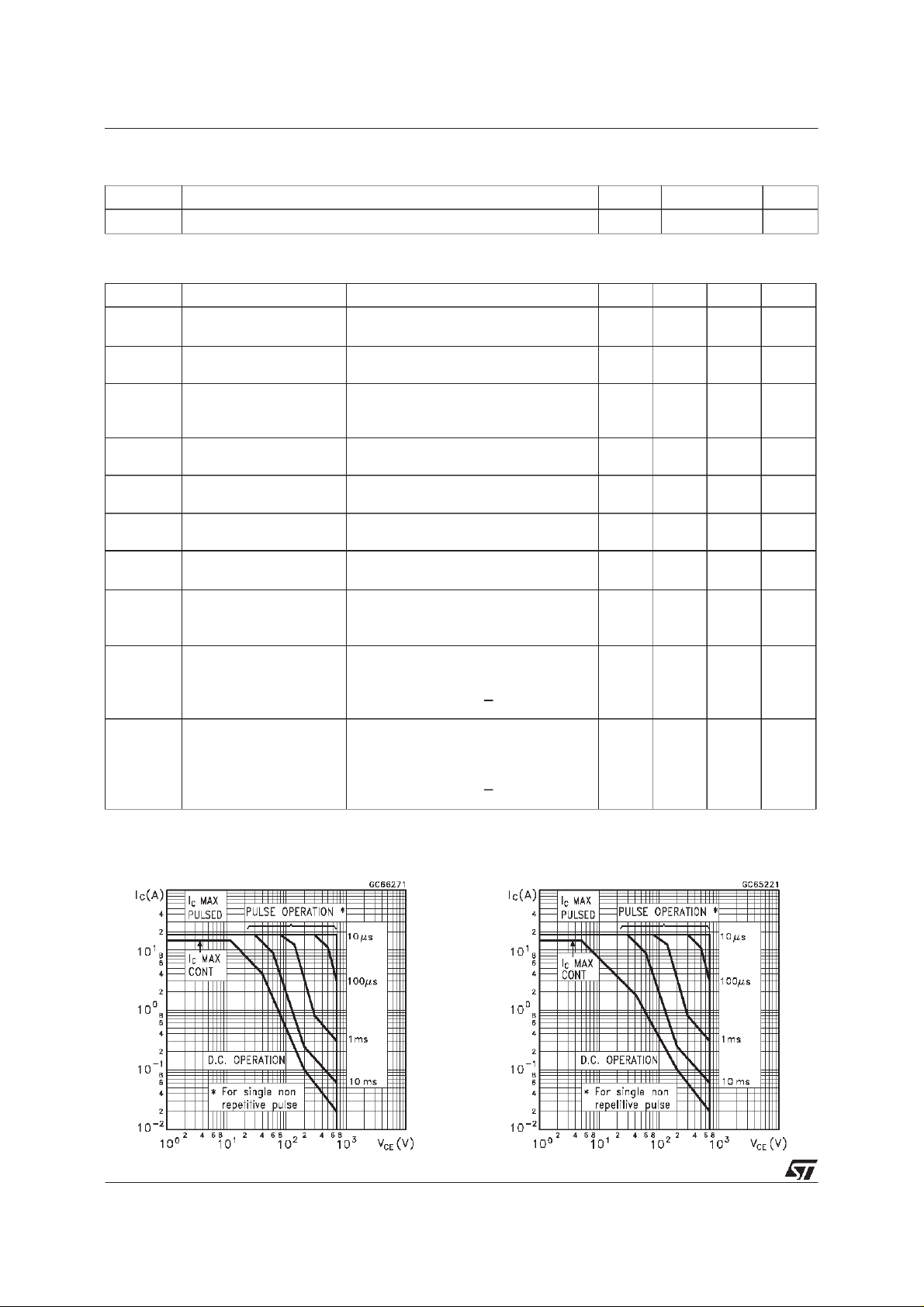
Safe OperatingArea For TO-218 Safe OperatingArea For ISOWATT218
2/8
Page 3

BUH1015/BUH1015HI
Thermal Impedancefor TO-218
DeratingCurve
ThermalImpedance for ISOWATT218
DCCurrent Gain
CollectorEmitter SaturationVoltage
BaseEmitter Saturation Voltage
3/8
Page 4

BUH1015/BUH1015HI
PowerLosses at 64 KHz SwitchingTime Inductive Loadat 64KHz
(see figure2)
ReverseBiased SOA
BASEDRIVE INFORMATION
In order to saturate the power switch and reduce
conduction losses, adequate direct base current
has to be provided for the lowest gain hFEat
I
B1
T
= 100oC (line scan phase). On the other hand,
j
negative base current I
must be provided the
B2
transistor to turn off (retrace phase). Most of the
dissipation, especially in the deflection
application, occurs at switch-off so it is essential
to determine the value of I
power losses, fall time t
and, consequently, Tj.A
f
which minimizes
B2
new set of curves have been defined to give total
power losses, t
and tfas a function of IB1at 64
s
KHz scanning frequencies for choosing the
4/8
optimum drive. The test circuit is illustrated in
figure 1.
The values of L and C are calculated from the
followingequations:
C
)2=
1
2
1
L
√
C(V
C
CEfly
2
)
CEfly
1
L(I
2
ω=2πf=
Where IC= operating collector current, V
flyback voltage, f= frequency of oscillation during
retrace.
=
Page 5

Figure1: Inductive Load Switching TestCircuits.
Figure2: SwitchingWaveformsin a DeflectionCircuit
BUH1015/BUH1015HI
5/8
Page 6

BUH1015/BUH1015HI
TO-218 (SOT-93) MECHANICAL DATA
DIM.
MIN. TYP. MAX. MIN. TYP. MAX.
A 4.7 4.9 0.185 0.193
C 1.17 1.37 0.046 0.054
D 2.5 0.098
E 0.5 0.78 0.019 0.030
F 1.1 1.3 0.043 0.051
G 10.8 11.1 0.425 0.437
H 14.7 15.2 0.578 0.598
L2 – 16.2 – 0.637
L3 18 0.708
L5 3.95 4.15 0.155 0.163
L6 31 1.220
R – 12.2 – 0.480
Ø 4 4.1 0.157 0.161
mm inch
E
A
C
L5
D
L6
L3
L2
H
G
¯
F
R
123
P025A
6/8
Page 7

ISOWATT218 MECHANICAL DATA
BUH1015/BUH1015HI
DIM.
A 5.35 5.65 0.211 0.222
C 3.30 3.80 0.130 0.150
D 2.90 3.10 0.114 0.122
D1 1.88 2.08 0.074 0.082
E 0.75 0.95 0.030 0.037
F 1.05 1.25 0.041 0.049
F2 1.50 1.70 0.059 0.067
F3 1.90 2.10 0.075 0.083
G 10.80 11.20 0.425 0.441
H 15.80 16.20 0.622 0.638
L 9 0.354
L1 20.80 21.20 0.819 0.835
L2 19.10 19.90 0.752 0.783
L3 22.80 23.60 0.898 0.929
L4 40.50 42.50 1.594 1.673
L5 4.85 5.25 0.191 0.207
L6 20.25 20.75 0.797 0.817
N 2.1 2.3 0.083 0.091
R 4.6 0.181
DIA 3.5 3.7 0.138 0.146
MIN. TYP. MAX. MIN. TYP. MAX.
mm inch
- Weight : 4.9 g (typ.)
- Maximum Torque (applied to mounting flange) Recommended: 0.8 Nm; Maximum: 1 Nm
- The side of the dissipator must be flat within 80 µm
P025C/A
7/8
Page 8

BUH1015/BUH1015HI
Information furnished is believed to be accurate and reliable. However, STMicroelectronics assumes no responsibility for the consequences
of use of such information nor for any infringement of patents or other rights of third parties which may result from its use. No license is
granted by implication or otherwise underany patent or patent rights of STMicroelectronics. Specification mentioned in this publication are
subject tochange without notice. This publication supersedes and replaces all information previously supplied. STMicroelectronics products
are notauthorized for use as critical components in life support devices or systems without express written approval of STMicroelectronics.
The ST logo is a trademark of STMicroelectronics
1999 STMicroelectronics – Printed in Italy – All Rights Reserved
STMicroelectronicsGROUP OF COMPANIES
Australia - Brazil - China - Finland - France - Germany - Hong Kong - India - Italy- Japan - Malaysia - Malta - Morocco -
Singapore- Spain - Sweden - Switzerland -United Kingdom - U.S.A.
http://www.st.com
.
8/8
 Loading...