

Datasheet BUF634U, BUF634T, BUF634P, BUF634F-500, BUF634 Datasheet (Burr Brown Corporation)
...Page 1

®
BUF634
BUF634
BUF634
BUF634
250mA HIGH-SPEED BUFFER
FEATURES
● HIGH OUTPUT CURRENT: 250mA
● SLEW RATE: 2000V/
● PIN-SELECTED BANDWIDTH:
30MHz to 180MHz
● LOW QUIESCENT CURRENT:
1.5mA (30MHz BW)
● WIDE SUPPLY RANGE:
● INTERNAL CURRENT LIMIT
● THERMAL SHUTDOWN PROTECTION
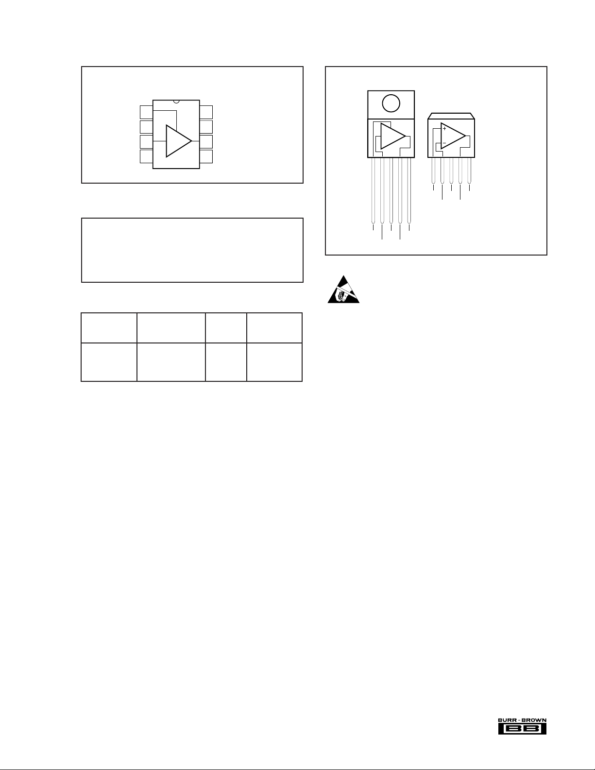
● 8-PIN DIP, SO-8, 5-LEAD TO-220, 5-LEAD
DDPAK SURFACE-MOUNT
µs
±2.25 to ±18V
BUF634
APPLICATIONS
● VALVE DRIVER
● SOLENOID DRIVER
● OP AMP CURRENT BOOSTER
● LINE DRIVER
● HEADPHONE DRIVER
● VIDEO DRIVER
● MOTOR DRIVER
● TEST EQUIPMENT
● ATE PIN DRIVER
DESCRIPTION
The BUF634 is a high speed unity-gain open-loop
buffer recommended for a wide range of applications.
It can be used inside the feedback loop of op amps to
increase output current, eliminate thermal feedback
and improve capacitive load drive.
For low power applications, the BUF634 operates
on 1.5mA quiescent current with 250mA output,
2000V/µs slew rate and 30MHz bandwidth. Bandwidth can be adjusted from 30MHz to 180MHz by
connecting a resistor between V– and the BW Pin.
Output circuitry is fully protected by internal current
limit and thermal shut-down making it rugged and
easy to use.
International Airport Industrial Park • Mailing Address: PO Box 11400, Tucson, AZ 85734 • Street Address: 6730 S. Tucson Blvd., Tucson, AZ 85706 • Tel: (520) 746-1111 • Twx: 910-952-1111
Internet: http://www.burr-brown.com/ • FAXLine: (800) 548-6133 (US/Canada Only) • Cable: BBRCORP • Telex: 066-6491 • FAX: (520) 889-1510 • Immediate Product Info: (800) 548-6132
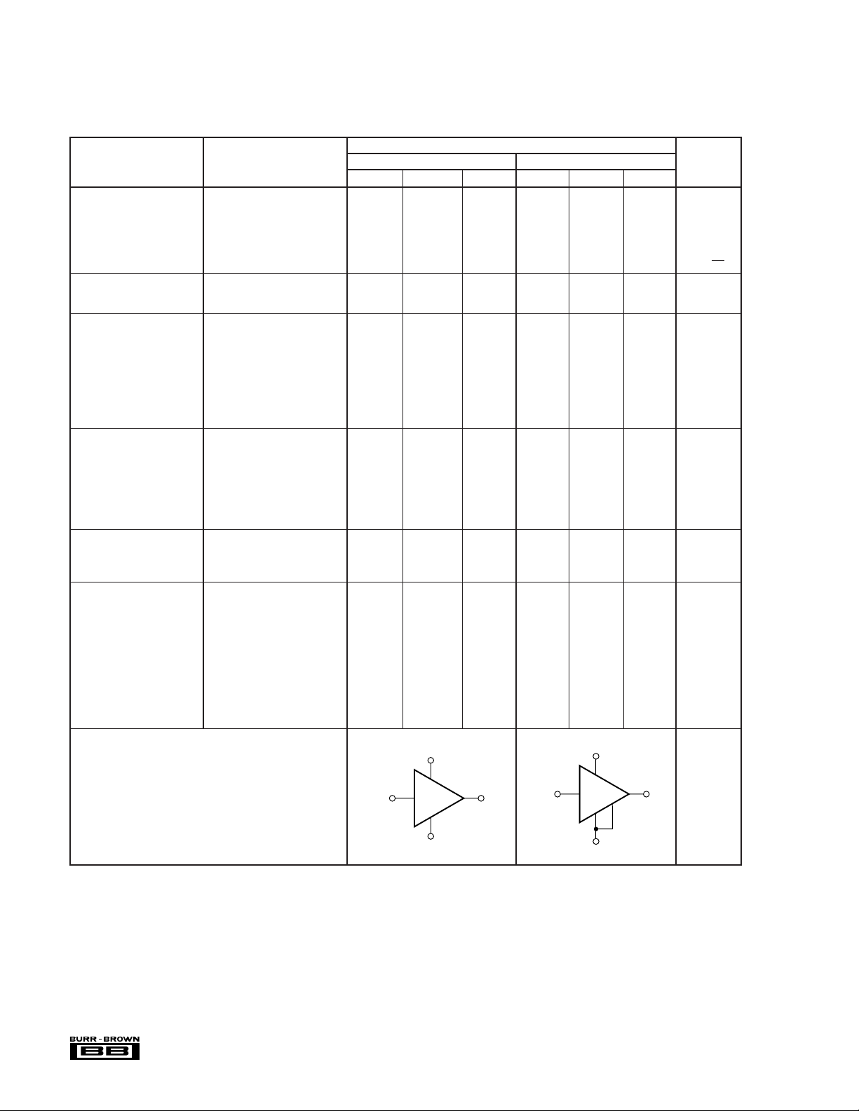
8-Pin DIP Package
SO-8 Surface-Mount Package
1
BW
2
NC
G = 1
3
V
IN
4
V–
8
NC
7
V+
6
V
O
5
NC
The BUF634 is available in a variety of packages to
suit mechanical and power dissipation requirements.
Types include 8-pin DIP, SO-8 surface-mount, 5-lead
TO-220, and a 5-lead DDPAK surface-mount plastic
power package.
5-Lead
TO-220
5-Lead DDPAK
Surface Mount
G = 1 G = 1
O
5
V+
1234
BW
NOTE: Tabs are connected
to V– supply.
5
V–
V+
V
V
IN
O
1234
BW
V–
V
IN
V
©
1993 Burr-Brown Corporation PDS-1206C Printed in U.S.A. June, 1996
Page 2
SPECIFICATIONS
BW
V+
V–
V
O
V
IN
ELECTRICAL
At T
A
= +25°C
(1)
, VS = ±15V, unless otherwise noted.
BUF634P, U, T, F
LOW QUIESCENT CURRENT MODE WIDE BANDWIDTH MODE
PARAMETER CONDITION MIN TYP MAX MIN TYP MAX UNITS
INPUT
Offset Voltage ±30 ±100 ✻✻ mV
vs Temperature Specified Temperature Range ±100 ✻ µV/°C
vs Power Supply V
Input Bias Current V
S
Input Impedance R
Noise Voltage f = 10kHz 4 ✻ nV/√Hz
GAIN R
R
L
R
(2)
= ±2.25V
= 1kΩ, VO = ±10V 0.95 0.99 ✻✻ V/V
L
= 100Ω, VO = ±10V 0.85 0.93 ✻✻ V/V
= 67Ω, VO = ±10V 0.8 0.9 ✻✻ V/V
L
to ±18V 0.1 1 ✻✻mV/V
= 0V ±0.5 ±2 ±5 ±20 µA
IN
= 100Ω 80 || 8 8 || 8 MΩ || pF
L
OUTPUT
Current Output, Continuous ±250 ✻ mA
Voltage Output, Positive I
Negative I
Positive I
Negative I
Positive I
Negative I
= 10mA (V+) –2.1 (V+) –1.7 ✻✻ V
O
= –10mA (V–) +2.1 (V–) +1.8 ✻✻ V
O
= 100mA (V+) –3 (V+) –2.4 ✻✻ V
O
= –100mA (V–) +4 (V– ) +3.5 ✻✻ V
O
= 150mA (V+) –4 (V+) –2.8 ✻✻ V
O
= –150mA (V–) +5 (V–) +4 ✻✻ V
O
Short-Circuit Current ±350 ±550 ±400 ✻ mA
DYNAMIC RESPONSE
Bandwidth, –3dB R
Slew Rate 20Vp-p, R
Settling Time, 0.1% 20V Step, R
1% 20V Step, R
Differential Gain
Differential Phase
3.58MHz, VO = 0.7V, RL = 150Ω
3.58MHz, VO = 0.7V, RL = 150Ω
= 1kΩ 30 180 MHz
L
R
= 100Ω 20 160 MHz
L
= 100Ω 2000 ✻ V/µs
L
= 100Ω 200 ✻ ns
L
= 100Ω 50 ✻ ns
L
4 0.4 %
2.5 0.1 °
POWER SUPPLY
Specified Operating Voltage ±15 ✻ V
Operating Voltage Range ±2.25
Quiescent Current, I
Q
IO = 0 ±1.5 ± 2 ±15 ±20 mA
(2)
±18 ✻✻V
TEMPERATURE RANGE
Specification –40 +85 ✻✻°C
Operating –40 +125 ✻✻°C
Storage –55 +125 ✻✻°C
Thermal Shutdown
Temperature, T
Thermal Resistance,
J
θ
JA
θ
JA
θ
JA
θ
JC
θ
JA
θ
JC
“P” Package
“U” Package
“T” Package
“T” Package 6 ✻ °C/W
“F” Package
“F” Package 6 ✻ °C/W
(3)
(3)
(3)
(3)
175 ✻ °C
100 ✻ °C/W
150 ✻ °C/W
65 ✻ °C/W
65 ✻ °C/W
V+
V
IN
V
O
V–
✻ Specifications the same as Low Quiescent Mode.
NOTES: (1) Tests are performed on high speed automatic test equipment, at approximately 25°C junction temperature. The power dissipation of this product will
cause some parameters to shift when warmed up. See typical performance curves for over-temperature performance. (2) Limited output swing available at low supply
voltage. See Output voltage specifications. (3) Typical when all leads are soldered to a circuit board. See text for recommendations.
The information provided herein is believed to be reliable; however, BURR-BROWN assumes no responsibility for inaccuracies or omissions. BURR-BROWN
assumes no responsibility for the use of this information, and all use of such information shall be entirely at the user’s own risk. Prices and specifications are subject
to change without notice. No patent rights or licenses to any of the circuits described herein are implied or granted to any third party. BURR-BROWN does not
authorize or warrant any BURR-BROWN product for use in life support devices and/or systems.
®
BUF634
2
Page 3
PIN CONFIGURATION
Top View 8-Pin Dip Package
1
BW
2
NC
G = 1
3
V
IN
4
V–
SO-8 Surface-Mount Package
8
NC
7
V+
6
V
O
5
NC
NC = No Connection
ABSOLUTE MAXIMUM RATINGS
Supply Voltage ..................................................................................... ±18V
Input Voltage Range ...............................................................................±V
Output Short-Circuit (to ground) .................................................Continuous
Operating Temperature .....................................................–40°C to +125°C
Storage Temperature ........................................................ –55°C to +125°C
Junction Temperature ....................................................................... +150°C
Lead Temperature (soldering,10s) .................................................... +300°C
PACKAGE/ORDERING INFORMATION
PACKAGE
DRAWING TEMPERATURE
PRODUCT PACKAGE NUMBER
BUF634P 8-Pin Plastic DIP 006 –40°C to +85°C
BUF634U SO-8 Surface-Mount 182 –40°C to +85°C
BUF634T 5-Lead TO-220 315 –40°C to +85°C
BUF634F 5-Lead DDPAK 325 –40°C to +85°C
NOTE: (1) For detailed drawing and dimension table, please see end of data
sheet, or Appendix C of Burr-Brown IC Data Book.
(1)
RANGE
Top View
5-Lead
TO-220
5-Lead DDPAK
Surface Mount
G = 1 G = 1
O
5
V+
1234
BW
V–
V
IN
5
V+
V
O
NOTE: Tab electrically
connected to V–.
1234
S
BW
V–
V
V
IN
ELECTROSTATIC
DISCHARGE SENSITIVITY
Any integrated circuit can be damaged by ESD. Burr-Brown
recommends that all integrated circuits be handled with
appropriate precautions. Failure to observe proper handling
and installation procedures can cause damage.
ESD damage can range from subtle performance degradation to complete device failure. Precision integrated circuits
may be more susceptible to damage because very small
parametric changes could cause the device not to meet
published specifications.
®
3
BUF634
Page 4

TYPICAL PERFORMANCE CURVES
At TA = +25°C, VS = ±15V, unless otherwise noted.
GAIN and PHASE vs FREQUENCY
vs QUIESCENT CURRENT
0
–10
–20
–30
Phase (°)
–40
IQ = 15mA
= 9mA
I
Q
= 4mA
I
Q
= 2.5mA
I
Q
= 1.5mA
I
Q
–50
1M 10M 100M 1G
Frequency (Hz)
GAIN and PHASE vs FREQUENCY
vs SOURCE RESISTANCE
Wide BW
Low I
Q
0
–10
–20
–30
Phase (°)
–40
Low I
Q
Wide BW
RS = 0Ω
= 50Ω
R
S
= 100Ω
R
S
–50
1M 10M 100M 1G
Frequency (Hz)
RL = 100Ω
= 50Ω
R
S
= 10mV
V
O
RL = 100Ω
= 10mV
V
O
10
5
0
–5
–10
–15
10
5
0
–5
–10
–15
Gain (dB)
Gain (dB)
GAIN and PHASE vs FREQUENCY
vs TEMPERATURE
Low I
Q
0
Wide BW
Wide BW
–10
–20
–30
Phase (°)
–40
Low I
Q
TJ = –40°C
= 25°C
T
J
= 125°C
T
J
–50
1M 10M 100M 1G
Frequency (Hz)
GAIN and PHASE vs FREQUENCY
vs LOAD RESISTANCE
Wide BW
Low I
Q
0
–10
–20
–30
Phase (°)
–40
Low I
Q
Wide BW
RL = 1kΩ
= 100Ω
R
L
= 50Ω
R
L
–50
1M 10M 100M 1G
Frequency (Hz)
RL = 100Ω
= 50Ω
R
S
= 10mV
V
O
RS = 50Ω
= 10mV
V
O
10
5
0
–5
–10
–15
10
5
0
–5
–10
–15
Gain (dB)
Gain (dB)
GAIN and PHASE vs FREQUENCY
vs LOAD CAPACITANCE
Low IQ Mode
0
–10
–20
–30
Phase (°)
–40
CL = 0pF
= 50pF
C
L
= 200pF
C
L
= 1nF
C
L
–50
1M 10M 100M 1G
Frequency (Hz)
®
BUF634
RL = 100Ω
= 50Ω
R
S
= 10mV
V
O
10
5
0
–5
–10
–15
Gain (dB)
4
GAIN and PHASE vs FREQUENCY
vs LOAD CAPACITANCE
Wide BW Mode
0
–10
–20
–30
Phase (°)
–40
CL = 0
= 50pF
C
L
= 200pF
C
L
= 1nF
C
L
–50
1M 10M 100M 1G
Frequency (Hz)
RL = 100Ω
= 50Ω
R
S
= 10mV
V
O
1
5
0
–5
–10
–15
0
Gain (dB)
Page 5

QUIESCENT CURRENT vs TEMPERATURE
20
15
10
5
0
Junction Temperature (°C)
–50 –25 0 25 50 75 100 125 150 175 200
Thermal Shutdown
≈10°C
Cooling
Wide BW Mode
Quiescent Current (mA)
TYPICAL PERFORMANCE CURVES (CONT)
q
)
SHORT CIRCUIT CURRENT vs TEMPERATURE
500
450
400
350
300
250
200
–50 –25 0 25 50 75 100 125 150
Junction Temperature (°C)
Wide Bandwidth Mode
Low IQ Mode
Limit Current (mA)
At TA = +25°C, VS = ±15V, unless otherwise noted.
GAIN and PHASE vs FREQUENCY
vs POWER SUPPLY VOLTAGE
Wide BW
Low I
Q
0
–10
–20
–30
Phase (°)
–40
Low I
Q
Wide BW
VS = ±18V
= ±12V
V
S
= ±5V
V
S
= ±2.25V
V
S
–50
1M 10M 100M 1G
Frequency (Hz)
QUIESCENT CURRENT
vs BANDWIDTH CONTROL RESISTANCE
20
18
16
14
15mA at R = 0
12
10
8
6
Quiescent Current (mA)
4
2
0
10 100 1k 10k
1.5mA at R = ∞
Resistance (Ω)
RL = 100Ω
= 50Ω
R
S
= 10mV
V
O
+15V
BW
R
–15V
10
5
0
–5
–10
–15
Gain (dB)
100
POWER SUPPLY REJECTION vs FREQUENCY
90
80
70
Wide BW
60
50
40
Low I
30
20
Power Supply Rejection (dB)
10
Q
0
1k 10k 100k 1M 10M
uency (Hz
Fre
7
QUIESCENT CURRENT vs TEMPERATURE
6
Low IQ Mode
5
4
3
2
Quiescent Current (mA)
1
0
–50 –25 0 25 50 75 100 125 150 175 200
Junction Temperature (°C)
Cooling
≈10°C
Thermal Shutdown
®
5
BUF634
Page 6

TYPICAL PERFORMANCE CURVES (CONT)
At TA = +25°C, VS = ±15V, unless otherwise noted.
OUTPUT VOLTAGE SWING vs OUTPUT CURRENT
13
VIN = 13V
12
11
VS = ±15V
10
–10
Low I
Mode
Q
–11
Output Voltage Swing (V)
–12
VIN = –13V
–13
0 50 100 150 200 250 300
TJ = –40°C
= 25°C
T
J
= 125°C
T
J
|Output Current| (mA)
MAXIMUM POWER DISSIPATION vs TEMPERATURE
3
2
8-Pin DIP
θ
= 100°C/W
JA
TO-220 and DDPAK
Free Air
θ
= 65°C/W
JA
1
Power Dissipation (W)
SO-8
= 150°C/W
θ
JA
0
–50 –25 0 25 50 75 100 125 150
Ambient Temperature (°C)
OUTPUT VOLTAGE SWING vs OUTPUT CURRENT
13
VIN = 13V
12
11
VS = ±15V
10
Wide BW Mode
–10
–11
Output Voltage Swing (V)
–12
VIN = –13V
–13
0 50 100 150 200 250 300
TJ = –40°C
= 25°C
T
J
= 125°C
T
J
|Output Current| (mA)
MAXIMUM POWER DISSIPATION vs TEMPERATURE
12
10
TO-220 and DDPAK
Infinite Heat Sink
θ
= 6°C/W
JC
8
6
4
Power Dissipation (W)
TO-220 and DDPAK
Free Air
θ
= 65°C/W
JA
2
0
–50 –25 0 25 50 75 100 125 150
Ambient Temperature (°C)
Input
Wide BW
Mode
Low I
Mode
SMALL-SIGNAL RESPONSE
RS = 50Ω, RL = 100Ω
LARGE-SIGNAL RESPONSE
R
= 50Ω, RL = 100Ω
S
Input
100mV/div 10V/div
Wide BW
Mode
Q
Low I
Mode
Q
20ns/div 20ns/div
®
BUF634
6
Page 7

APPLICATION INFORMATION
Figure 1 is a simplified circuit diagram of the BUF634
showing its open-loop complementary follower design.
V+
Thermal
Shutdown
200Ω
V
IN
(1)
I
1
150Ω
4kΩ
BW
Signal path indicated in bold.
Note: (1) Stage currents are set by I
V–
.
1
FIGURE 1. Simplified Circuit Diagram.
Figure 2 shows the BUF634 connected as an open-loop
buffer. The source impedance and optional input resistor,
RS, influence frequency response—see typical curves. Power
supplies should be bypassed with capacitors connected close
to the device pins. Capacitor values as low as 0.1µF will
assure stable operation in most applications, but high output
current and fast output slewing can demand large current
transients from the power supplies. Solid tantalum 10µF
capacitors are recommended.
High frequency open-loop applications may benefit from
special bypassing and layout considerations—see “High
Frequency Applications” at end of applications discussion.
V+
10µF
DIP/SO-8
Pinout shown
10µF
3
BUF634
7
6
1
4
Optional connection for
wide bandwidth — see text.
V–
V
O
R
L
R
V
S
IN
FIGURE 2. Buffer Connections.
V
O
OUTPUT CURRENT
The BUF634 can deliver up to ±250mA continuous output
current. Internal circuitry limits output current to approximately ±350mA—see typical performance curve “Short
Circuit Current vs Temperature”. For many applications,
however, the continuous output current will be limited by
thermal effects.
The output voltage swing capability varies with junction
temperature and output current—see typical curves “Output
Voltage Swing vs Output Current.” Although all four package types are tested for the same output performance using
a high speed test, the higher junction temperatures with the
DIP and SO-8 package types will often provide less output
voltage swing. Junction temperature is reduced in the DDPAK
surface-mount power package because it is soldered directly
to the circuit board. The TO-220 package used with a good
heat sink further reduces junction temperature, allowing
maximum possible output swing.
THERMAL PROTECTION
Power dissipated in the BUF634 will cause the junction
temperature to rise. A thermal protection circuit in the
BUF634 will disable the output when the junction temperature reaches approximately 175°C. When the thermal protection is activated, the output stage is disabled, allowing the
device to cool. Quiescent current is approximately 6mA
during thermal shutdown. When the junction temperature
cools to approximately 165°C the output circuitry is again
enabled. This can cause the protection circuit to cycle on and
off with a period ranging from a fraction of a second to
several minutes or more, depending on package type, signal,
load and thermal environment.
The thermal protection circuit is designed to prevent damage
during abnormal conditions. Any tendency to activate the
thermal protection circuit during normal operation is a sign
of an inadequate heat sink or excessive power dissipation for
the package type.
TO-220 package provides the best thermal performance.
When the TO-220 is used with a properly sized heat sink,
output is not limited by thermal performance. See Application Bulletin AB-037 for details on heat sink calculations.
The DDPAK also has excellent thermal characteristics. Its
mounting tab should be soldered to a circuit board copper
area for good heat dissipation. Figure 3 shows typical
thermal resistance from junction to ambient as a function of
the copper area. The mounting tab of the TO-220 and
DDPAK packages is electrically connected to the V– power
supply.
The DIP and SO-8 surface-mount packages are excellent for
applications requiring high output current with low average
power dissipation. To achieve the best possible thermal
performance with the DIP or SO-8 packages, solder the
device directly to a circuit board. Since much of the heat is
dissipated by conduction through the package pins, sockets
will degrade thermal performance. Use wide circuit board
traces on all the device pins, including pins that are not
connected. With the DIP package, use traces on both sides
of the printed circuit board if possible.
7
BUF634
®
Page 8

THERMAL RESISTANCE vs
60
50
(°C/W)
JA
40
30
20
Thermal Resistance, θ
10
012345
CIRCUIT BOARD COPPER AREA
BUF634F
Surface Mount Package
1oz copper
2
Copper Area (inches
)
FIGURE 3. Thermal Resistance vs Circuit Board Copper Area.
Circuit Board Copper Area
BUF634F
Surface Mount Package
POWER DISSIPATION
Power dissipation depends on power supply voltage, signal
and load conditions. With DC signals, power dissipation is
equal to the product of output current times the voltage
across the conducting output transistor, V
– VO. Power
S
dissipation can be minimized by using the lowest possible
power supply voltage necessary to assure the required output
voltage swing.
For resistive loads, the maximum power dissipation occurs
at a DC output voltage of one-half the power supply voltage.
Dissipation with AC signals is lower. Application Bulletin
AB-039 explains how to calculate or measure power dissipation with unusual signals and loads.
Any tendency to activate the thermal protection circuit
indicates excessive power dissipation or an inadequate heat
sink. For reliable operation, junction temperature should be
limited to 150°C, maximum. To estimate the margin of
safety in a complete design, increase the ambient temperature until the thermal protection is triggered. The thermal
protection should trigger more than 45°C above the maximum expected ambient condition of your application.
INPUT CHARACTERISTICS
Internal circuitry is protected with a diode clamp connected
from the input to output of the BUF634—see Figure 1. If the
output is unable to follow the input within approximately 3V
(such as with an output short-circuit), the input will conduct
increased current from the input source. This is limited by
the internal 200Ω resistor. If the input source can be damaged by this increase in load current, an additional resistor
can be connected in series with the input.
BANDWIDTH CONTROL PIN
The –3dB bandwidth of the BUF634 is approximately 30MHz
in the low quiescent current mode (1.5mA typical). To select
this mode, leave the bandwidth control pin open (no connection).
Bandwidth can be extended to approximately 180MHz by
connecting the bandwidth control pin to V–. This increases
®
BUF634
the quiescent current to approximately 15mA. Intermediate
bandwidths can be set by connecting a resistor in series with
the bandwidth control pin—see typical curve "Quiescent
Current vs Resistance" for resistor selection. Characteristics
of the bandwidth control pin can be seen in the simplified
circuit diagram, Figure 1.
The rated output current and slew rate are not affected by the
bandwidth control, but the current limit value changes slightly.
Output voltage swing is somewhat improved in the wide
bandwidth mode. The increased quiescent current when in
wide bandwidth mode produces greater power dissipation
during low output current conditions. This quiescent power
is equal to the total supply voltage, (V+) + |(V–)|, times the
quiescent current.
BOOSTING OP AMP OUTPUT CURRENT
The BUF634 can be connected inside the feedback loop of
most op amps to increase output current—see Figure 4.
When connected inside the feedback loop, the BUF634’s
offset voltage and other errors are corrected by the feedback
of the op amp.
To assure that the op amp remains stable, the BUF634’s
phase shift must remain small throughout the loop gain of
the circuit. For a G=+1 op amp circuit, the BUF634 must
contribute little additional phase shift (approximately 20° or
less) at the unity-gain frequency of the op amp. Phase shift
is affected by various operating conditions that may affect
stability of the op amp—see typical Gain and Phase curves.
Most general-purpose or precision op amps remain unitygain stable with the BUF634 connected inside the feedback
loop as shown. Large capacitive loads may require the
BUF634 to be connected for wide bandwidth for stable
operation. High speed or fast-settling op amps generally
require the wide bandwidth mode to remain stable and to
assure good dynamic performance. To check for stability
with an op amp, look for oscillations or excessive ringing on
signal pulses with the intended load and worst case conditions that affect phase response of the buffer.
8
Page 9

HIGH FREQUENCY APPLICATIONS
The BUF634’s excellent bandwidth and fast slew rate make it
useful in a variety of high frequency open-loop applications.
When operated open-loop, circuit board layout and bypassing
technique can affect dynamic performance.
For best results, use a ground plane type circuit board layout
and bypass the power supplies with 0.1µF ceramic chip
V+
(1)
C
1
V
V
IN
NOTE: (1) C
for most common op amps.
Use with unity-gain stable
high speed op amps.
OPA
not required
1
BUF634
BW
V–
O
Wide BW mode
(if required)
FIGURE 4. Boosting Op Amp Output Current.
capacitors at the device pins in parallel with solid tantalum
10µF capacitors. Source resistance will affect high-frequency
peaking and step response overshoot and ringing. Best
response is usually achieved with a series input resistor of
25Ω to 200Ω, depending on the signal source. Response
with some loads (especially capacitive) can be improved
with a resistor of 10Ω to 150Ω in series with the output.
OP AMP RECOMMENDATIONS
OPA177, OPA1013 Use Low I
OPA111, OPA2111
OPA121, OPA234
OPA130
OPA27, OPA2107 Low IQ mode is stable. Increasing CL may cause
OPA602, OPA131
OPA627, OPA132
OPA637, OPA37 Use Wide BW mode. These op amps are not G = 1
NOTE: (1) Single, dual, and quad versions.
(1)
(1)
,
(1)
excessive ringing or instability. Use Wide BW mode.
(1)
Use Wide BW mode, C1 = 200pF. G = 1 stable.
stable. Use in G > 4.
mode. G = 1 stable.
Q
G = +21
250Ω
1µF
V
IN
OPA132
100kΩ
FIGURE 5. High Performance Headphone Driver.
+24V
10kΩ
+
10µF
BUF634
10kΩ
NOTE: (1) System bypass capacitors.
(1)
C
(1)
C
FIGURE 6. Pseudo-Ground Driver.
+
12V
12V
–
+
–
5kΩ
pseudo
ground
V+
BW
Drives headphones
or small speakers.
RL = 100Ω
f
1kHz
20kHz
V
IN
±2V
THD+N
0.015%
0.02%
OPA177
BUF634
V–
FIGURE 7. Current-Output Valve Driver.
10kΩ
BUF634
= ±200mA
I
O
Valve
10Ω
1kΩ
1/2
V
±1V
IN
OPA2234
FIGURE 8. Bridge-Connected Motor Driver.
9kΩ
BUF634
Motor
±20V
at 250mA
9
BUF634
10kΩ
1/2
OPA2234
®
BUF634
 Loading...