

Page 1
MEDIUM VOLTAGE NPN FAST-SWITCHING
■ SGS-THOMS O N PREF ERRE D SA LES TYP E
■ NPN DARLINGTON
■ LOW BASE-DRIVE REQUIREMENTS
■ FAST SWITCHING SPEED
■ INTEGRATED ANTIPARALLEL
COLLECTOR-EMITTER DIODE
APPLICATIONS
■ HORIZONTAL DEFLECTION FOR
MONOCH R OM E TVs
■ GENERAL PURPOSE SWITCHING
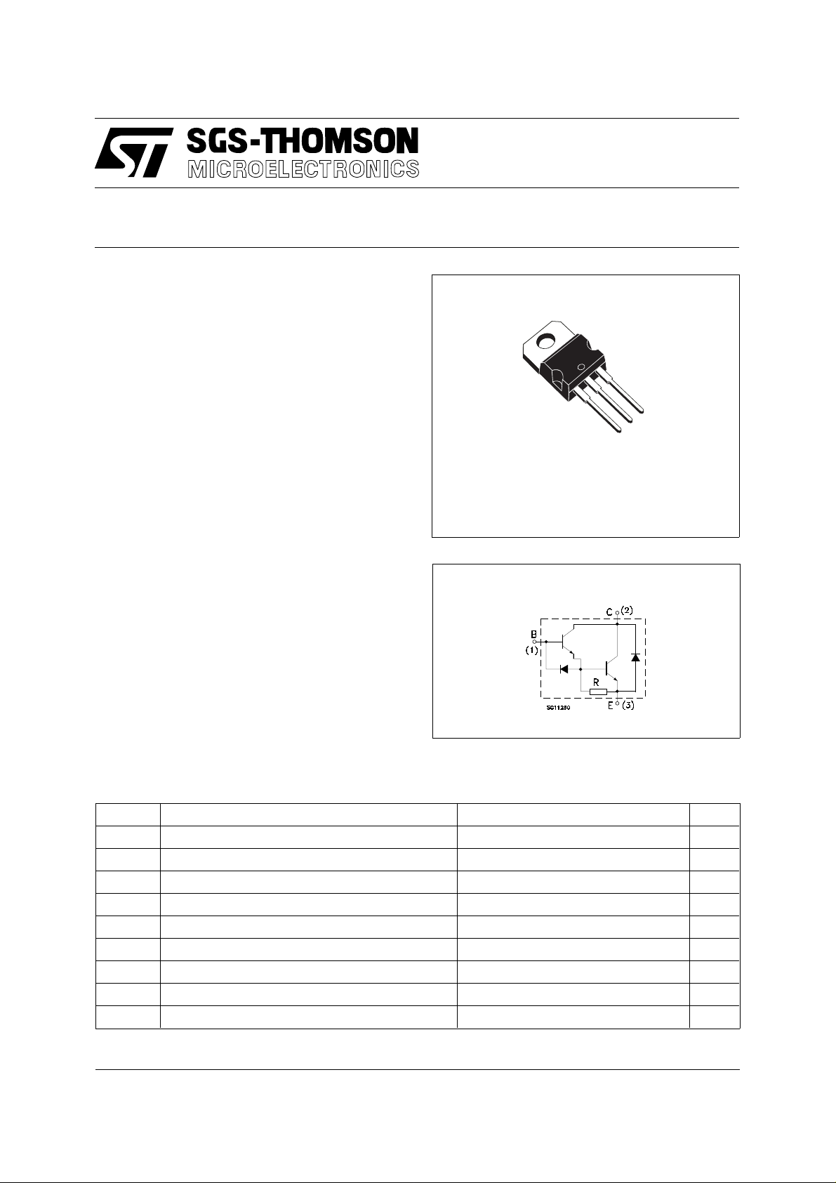
BU810
DARLINGTON TRANSISTOR
3
2
1
DESCRIPTION
TO-220
The BU810 is a Multiepitaxial Planar NPN
Transistor in TO-220 package. It is intended for
use in high frequency and efficency converters,
switching regulators and motor control.
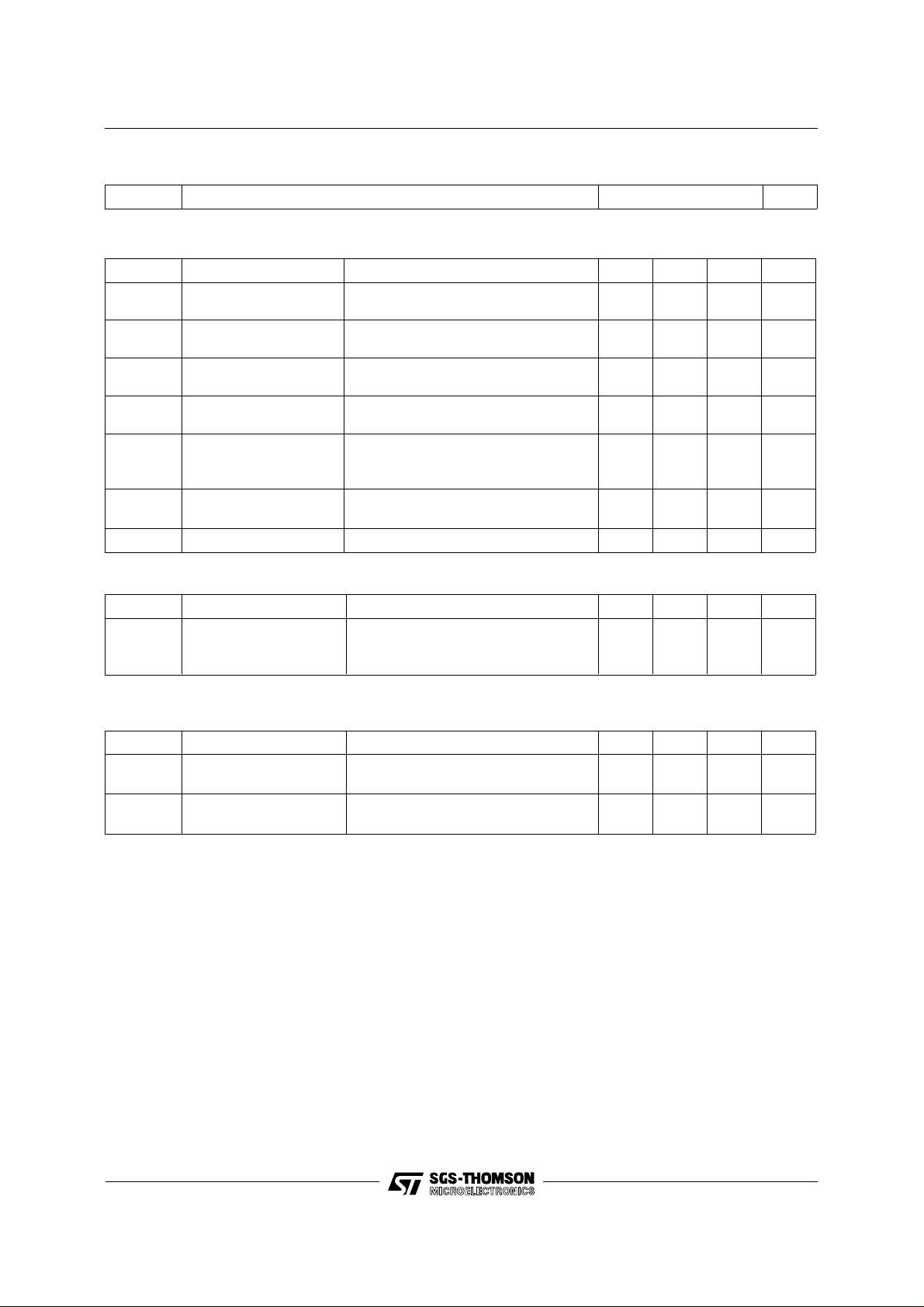
INTERNAL SCHEMATIC DIAGRAM
R = 200 Ω
ABSOL UT E MAXIMU M RATINGS
Symbol Parameter Value Unit
V
V
V
I
P
T
Collector-Base Voltage (IE = 0) 600 V
CBO
Collector-Emitter Voltage (IB = 0) 400 V
CEO
Emitter-Base Voltage (IC = 0) 5 V
EBO
I
Collector Current 7 A
C
Collector Peak Current 10 A
CM
I
Base Current 2 A
B
Total Power Dissipation at T
tot
Storage Temperature -65 to 150
stg
T
Junction Temperature 150
j
≤ 25 oC75W
case
o
C
o
C
June 1997
1/4
Page 2
BU810
THERMAL DATA
R
thj-case
Thermal Resistance Junction-case Max 1.66
o
C/W
ELECTRICAL CHARACTERISTICS (T
= 25 oC unless otherwise specified)
case
Symbol Parameter Test Conditions Min. Typ. Max. Unit
I
I
CES
CEO
Collector Cut-off
Current (V
BE
= 0)
Collector Cut-off
= 600 V 200 µA
V
CE
VCE = 400 V 1 mA
Current (IB = 0)
∗ Emitter Cut-off
I
EBO
Current (I
V
CEO(sus)
∗ Collector-Emitter
= 0)
C
= 5 V 150 mA
V
EB
IC = 0.1 A 400 V
Sustaining Voltage
V
CE(sat)
V
BE(sat)
∗ Collector-Emitter
Saturation Voltage
∗ Base-Emitter
Saturation Voltage
V
Diode Forward Voltage IF = 7 A 3 V
F
IC = 2 A IB = 20 mA
I
= 4 A IB = 200 mA
C
I
= 7 A IB = 0.7 A
C
IC = 2 A IB = 20 mA
I
= 4 A IB = 200 mA
C
2
2.5
3
2.2
3
RESIS TIVE SWITC H ING TIMES
Symbol Parameter Test Conditions Min. Typ. Max. Unit
t
t
on
s
t
f
Turn-on Time
Storage Time
Fall Time
V
= 250V IC = 2A IB1 = 20mA
Clamp
V
= -5 V
BE(off)
0.6
1.5
0.5
V
V
V
V
V
µs
µs
µs
INDUCTIVE SWIT CHING TIMES
Symbol Parameter Test Conditions Min. Typ. Max. Unit
t
t
* Pulsed : Pulse duration = 300 µs, duty cycle = 2%
s
t
f
s
t
f
Storage Time
Fall Time
Storage Time
Fall Time
V
= 250V IC = 2A IB1 = 20mA
Clamp
V
= -5 V L = 500µH
BE(off)
V
= 250V IC = 7A IB1 = 0.7A
Clamp
V
= -5 V L = 500µH
BE(off)
1.5
0.4
1.5
0.4
µs
µs
µs
µs
2/4
Page 3

E
TO-220 MECHANICAL DATA
BU810
DIM.
MIN. TYP. MAX. MIN. TYP. MAX.
A 4.40 4.60 0.173 0.181
C 1.23 1.32 0.048 0.051
D 2.40 2.72 0.094 0.107
D1 1.27 0.050
E 0.49 0.70 0.019 0.027
F 0.61 0.88 0.024 0.034
F1 1.14 1.70 0.044 0.067
F2 1.14 1.70 0.044 0.067
G 4.95 5.15 0.194 0.203
G1 2.4 2.7 0.094 0.106
H2 10.0 10.40 0.393 0.409
L2 16.4 0.645
L4 13.0 14.0 0.511 0.551
L5 2.65 2.95 0.104 0.116
L6 15.25 15.75 0.600 0.620
L7 6.2 6.6 0.244 0.260
L9 3.5 3.93 0.137 0.154
DIA. 3.75 3.85 0.147 0.151
mm inch
A
C
D
D1
L2
F1
L5
Dia.
G1
F
F2
L9
G
H2
L7
L6
L4
P011C
3/4
Page 4

BU810
Information furnished is believed to be accurate and reliable. However, SGS-THOMSON Microelectronics assumes no responsability for the
consequences of use of such information nor for any infringement of patents or other rights of third parties which may results from its use. No
license is granted by implication or ot h erwise under any patent or patent rights of SGS-THOMSON Microelectronics. Specifi cations mentioned
in this publication are subject to change without notice. This publication sup ersedes and replaces all information previously supplied.
SGS-THOMSON Microelectronics products are not authorized for use as critical components in life support devices or systems without express
written approval of SGS-THOMSON Microelectonics.
© 1997 SGS-THOMSON Microelectronics - Printed in Italy - All Rights Reserved
Australia - Brazil - Canada - China - France - Germany - Hong Kong - Italy - Japan - Korea - Malaysia - Malta - Morocco - The Netherlands -
Singapore - Spain - Sweden - Switzerland - Taiwan - Thailand - United Kingdom - U.S.A
SGS-THOMSON Microelectronics GROUP OF COMPANIES
. . .
4/4
 Loading...