

Page 1
1
Standard ICs
Quad analog switch
BU4066BC / BU4066BCF / BU4066BCFV
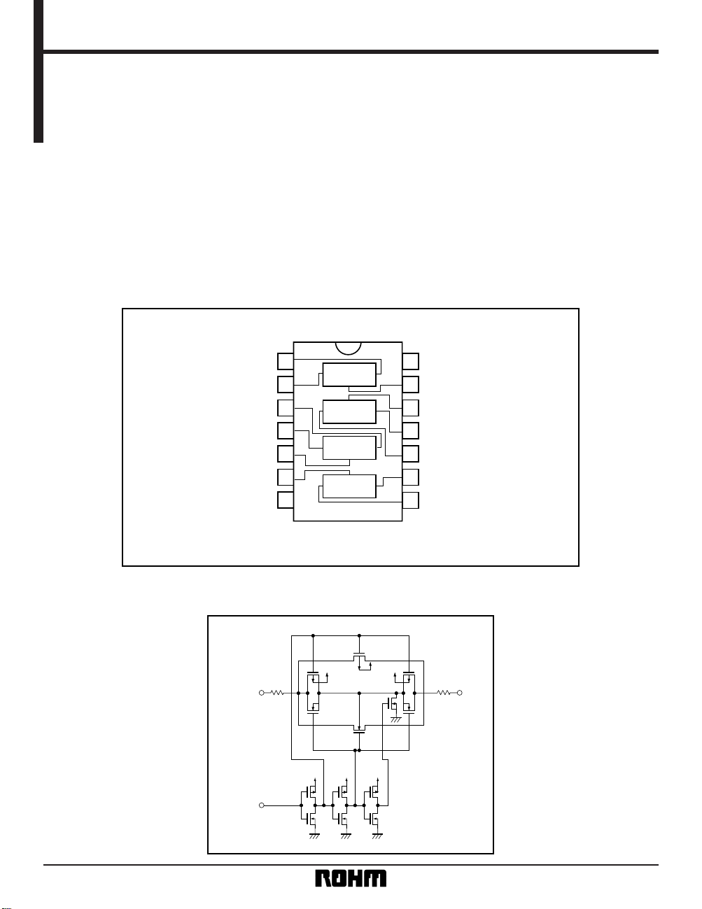
The BU4066BC, BU4066BCF, and BU4066BCFV each consist of four independent switches capable of controlling
either digital or analog signals. When Enable Input (CONT) is set to the “H” level, impedance is low (ON status)
between switch input and output, and when Enable Input (CONT) is set to the “L” level, impedance is high (OFF status). As the BU4066BC has a good propagation characteristic, it can control large input voltage amplitudes. These
switches can be used in analog and digital signal switching and in chopper modulator and demodulator circuits.
•
Logic circuit diagram
•
Block diagram
OUT / IN
V
DD VDD
VSS
VDD
IN / OUT
CONT
DIP / SOP / SSOP
SWA
OUT / IN IN / OUT
SWD
OUT / IN IN / OUT
SWB
IN / OUT OUT / IN
SWC
OUT / ININ / OUT
VDD
14
I / O1
1
C1
13
C4
12
I / O4
11
10
O / I3
9
I / O3
8
O / I1
2
O / I2
3
I / O2
4
C2
5
C3
6
Vss
7
O / I4
Page 2
2
Standard ICs BU4066BC / BU4066BCF / BU4066BCFV
•
Absolute maximum ratings (Ta = 25°C)
Parameter Symbol Limits Unit
Power supply voltage V
DD V
Power dissipation mW
Operating temperature °C
Storage temperature °C
Input voltage V
IN V
Topr
Tstg
Pd
– 0.5 ~ + 20
– 40 ~ + 85
– 55 ~ + 150
– 0.5 ~ V
DD + 0.5
1000 (DIP), 450(SOP)
350 (SSOP)
•
Electrical characteristics
DC characteristics (unless otherwise noted, Ta = 25°C, V
SS = 0V)
Parameter Symbol Min. Typ. Max. Unit Conditions
Measurement
circuit
Input high-level voltage V
IH
3.5 — —
V
5
—7.0 — — 10
11.0 — — 15
Input low-level voltage V
IL
— — 1.5
V
5
— Fig. 1— — 3.0 10
— — 3.75 15
Input high-level current — — 0.3 µA15V
IH
= 15V Fig. 1
Input low-level current I
IL
— — – 0.3 µA15V
IL
= 0V Fig. 1
ON resistance R
ON
— 150 600
Ω
5V
IN
= 0.25V, RL = 10kΩ
Fig. 1
— 500 950 5
— 200 600 5
— 230 500 10
— 180 280 15
ON resistance deflexion ∆R
ON
—25—
Ω
5
R
L
= 10kΩ
Fig. 1—10— 10
—5— 15
— — 0.3
µA
15 V
IN
= 15V, V
OUT
= 0V
Fig. 1
— — – 0.3 15 V
IN
= 0V, V
OUT
= 15V
Static current dissipation I
DD
— — 1.0
µA
5
V
I
= VDD or GND —— — 2.0 10
— — 4.0 15
C
C
— 8 — pF — f = 1MHz —
Input capacitance (switch input) C
S
— 10 — pF — f = 1MHz —
Fig. 1
I
IH
VIN = 2.5V, RL = 10kΩ
V
IN
= 5V, RL = 10kΩ
V
IN
= 5V, RL = 10kΩ
V
I
= VDD / 2
I
OFF
VIN = 7.5V, RL = 10kΩ
V
DD
(V)
OFF-channel
leakage current
Input capacitance (control input)
Page 3

3
Standard ICs BU4066BC / BU4066BCF / BU4066BCFV
•
Electrical characteristics
Switching characteristics (unless otherwise noted, Ta = 25°C, C
L = 50pF)
VSS = – 5V, RL = 10kΩ
– 50dB at channel off.
Parameter Symbol Min. Typ. Max. Unit Conditions
Measurement
circuit
Propagation delay time
SW IN→OUT
t
PLH
tPHL
—2050
ns
5
R
L
= 10kΩ Fig.210—1240
15—1030
Propagation delay time
CONT→OUT
t
PHZ
tPLZ
—4090
ns
5
R
L = 1kΩ
Fig.210—3580
15—3070
Propagation delay time
CONT→OUT
tPZH
tPZL
— 60 140
ns
5
R
L = 1kΩ
Fig.210—2050
15—1540
Feedthrough attenuation
FT — 0.7 — MHz 5 Fig.2
Sine wave distortion D — 0.1 — % 5 Fig.2
Crosstalk
CT
C — — 600 mVP-P 5
f = 1MHz
Fig.2
Crosstalk (2)
between channels
CT — 1 — MHz 5 Fig.2
V
DD (V)
Output “H”, “L”
Output “High -Z”→ “H”, “L”
∗
1 VIN : 5VP-P sine wave, frequency that enables
∗
2 VIN : 5VP-P sine wave.
V
OUT
VIN
VSS = – 5V, RL = 10kΩ
∗
1
VSS = – 5V, RL = 10kΩ
∗
2
VSS = – 5V, RL = 10kΩ
∗
1
→ “High-Z”
(CONT→OUT)
•
Measurement circuits
IIN
O / I
I / O
GND
CONT
A
V
DD
VOUT
RL
Fig. 1 (a) Input voltage, current
1
2
O / I
I / O
GND
CONT
VDD
VOUT
VDDVIN =
VIN
VOUT
RON = 10
R
L = 10kΩ
kΩ – 1
Fig. 1 (b) On resistance
O / I
CONT
GND
VDD
I / O
A
Fig. 1 (c) Channel off leakage current
Page 4

4
Standard ICs BU4066BC / BU4066BCF / BU4066BCFV
O / II / O
GND
CONT
P.G.
V
DD
CL
RL
Fig. 2 (a) Propagation delay time (IN to OUT)
O / I
I / O
CONT
GND
P.G.
V
DD
CL
RL
tPHZ tPZH
50% 50%
90%
50%
Fig. 2 (b) Propagation delay time
(CONT to OUT)
O / II / O
CONT
GND
P.G.
V
DD
CLRL
tPLZ tPZL
50%
50%
10%
50%
Fig. 2 (c) Propagation delay time
(CONT to OUT)
O / II / O
CONT
GND
VDD = 5V
5VP-P
CL
VSS = – 5V
R
L
~
Fig. 2 (d) Sine wave distortion, feedthrough attenuation
~
VDD = 5V
OSC
CL
RL
VSS = – 5V
CL
GND
R
L
RL
~
V
Fig. 2 (e) Crosstalk
O / I
I / O
CONT
GND
VDD = 5V
5V
P-P
CL
VSS = – 5V
1kΩ
RL
~
Fig. 2 (f) Control IN→OUT crosstalk
Page 5

5
Standard ICs BU4066BC / BU4066BCF / BU4066BCFV
6.5 ± 0.3
19.4 ± 0.3
0.5 ± 0.1
3.2 ± 0.2 4.25 ± 0.3
14 8
71
0.3 ± 0.1
0.51Min.
7.62
0° ~ 15°
2.54
DIP14 SOP14
SSOP-B14
BU4066BC BU4066BCF
BU4066BCFV
0.1
0.22 ± 0.1
0.65
8
7
14
1
6.4 ± 0.3
4.4 ± 0.2
5.0 ± 0.2
1.15 ± 0.1
0.15 ± 0.1
0.3Min.
0.1
0.4 ± 0.11.27
1
14
8.7 ± 0.2
7
8
4.4 ± 0.2
6.2 ± 0.3
0.11
1.5 ± 0.1
0.15
0.15 ± 0.1
0.3Min.
•
External dimensions (Units: mm)
•
Electrical characteristic curve
POWER DISSIPATION: Pd (mW)
AMBIENT TEMPERATURE: Ta (°C)
1200
1000
800
600
SOP - 14
SSOP - B14
400
200
0
0255075
100 125 150
DIP - 14
Fig. 3 Power dissipation vs.
ambient temperature
 Loading...