

Page 1
1
Standard ICs
8-channel analog multiplexer /
demultiplexer
BU4051BC / BU4051BCF / BU4051BCFV
The BU4051BC, BU4051BCF and BU4051BCFV are analog multiplexers / demultiplexers which use three-input digital signals for control via an 8-channel analog switch.
These products feature high on / off output voltage ratio and low crosstalk between analog switches.
•
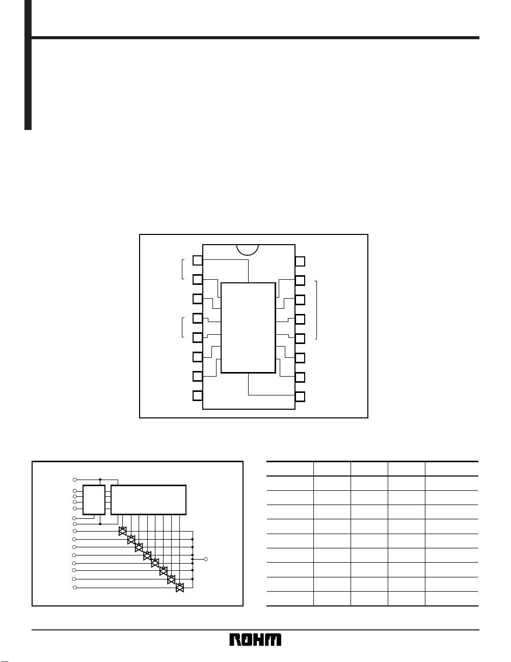
Block diagram
X4
CHANNEL
IN / OUT
COMMON
OUT / IN
1
X6
2
X
3
X7
4
X5
5
INH
6
VEE
7
VSS
8
16
15
14
13
12
11
10
9
VDD
X2
X1
X0
X3
A
B
C
C
X
6
X
X
7
X5
INH
V
EE
X2
X1
X0
X3
A
B
CHANNEL
IN / OUT
CHANNEL
IN / OUT
X4
•
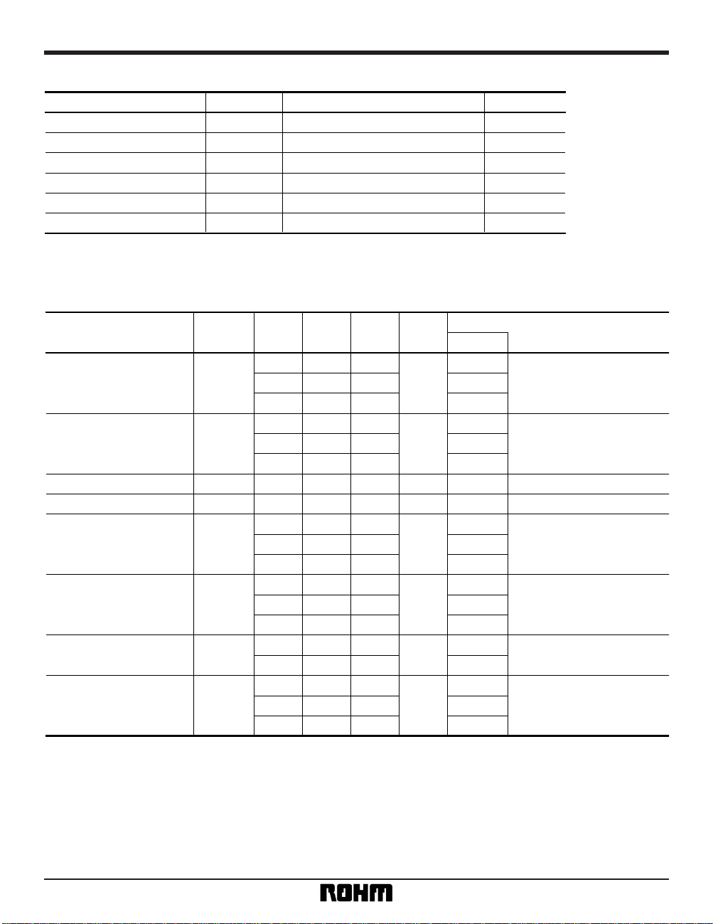
Logic circuit diagram
•
Truth table
INH A B C ON SWITCH
L LLL X
0
LHLL X1
L LHL X2
LHHLX3
LLLHX4
L HLH X5
LLHHX6
L HHH X7
H X X X NONE
X: Irrelevant
VDD (16)
INH (6)
A (11)
B (10)
C (9)
X0 (13)
X
1 (14)
X2 (15)
X3 (12)
X4 (1)
X5 (5)
X6 (2)
X
7 (4)
V
EE (7)
V
SS (8)
X
(3) COMMON
LEVEL
CONVERTER
BINARY TO 1 of
8
DECODER WITH INHIBIT
Page 2
2
Standard ICs BU4051BC / BU4051BCF / BU4051BCFV
•
Absolute maximum ratings (Ta = 25°C)
Parameter Symbol Limits Unit
Power supply voltage 2 V
DD—VEE V
Power supply voltage 1 V
DD – 0.5 ~ + 20
– 0.5 ~ + 20
– 40 ~ + 85
– 55 ~ + 150
V
Power dissipation Pd 1000 (DIP), 500 (SOP), 400 (SSOP) mW
Operating temperature Topr °C
Storage temperature Tstg °C
Input voltage V
IN – 0.5 ~ VDD + 0.5 V
•
Electrical characteristics
DC characteristics (unless otherwise noted, Ta = 25°C, V
EE = VSS = 0V)
Parameter Symbol Min. Typ. Max. Unit Conditions
Input high-level voltage V
IH
3.5 — —
V
5
—7.0 — — 10
11.0 — — 15
Input low-level voltage V
IL
— — 1.5
V
5
—— — 3.0 10
— — 4.0 15
Input high-level current I
IH — — 0.3 µA15VIH = 15V
Input low-level current I
IL — — – 0.3 µA15VIL = 0V
RON resistance R
ON
— — 950
Ω
5
— — 250 10
— — 160 15
RON resistance deflexion
—10—
Ω
5
——6— 10
—4— 15
OFF-channel
leakage current
I
OFF
— — 0.3
µA
15
—
— — – 0.3 15
Static current dissipation I
DD
—— 5
µA
5
V
I = VDD
VIN = VDD / 2
or GND— — 10 10
— — 15 15
V
DD (V)
∆R
ON
Page 3

3
Standard ICs BU4051BC / BU4051BCF / BU4051BCFV
Switching characteristics (unless otherwise noted, Ta = 25°C, VEE = VSS = 0V, RL = 1kΩ, CL = 50pF)
Parameter Symbol Min. Typ. Max. Unit Conditions
Measurement
circuit
t
PLH
t
PHL
—1545
ns
5
— Fig.4— 8 20 10
— 6 15 15
— 170 550
ns
5
—— 90 240 10
— 70 160 15
— 150 380
ns
5
—— 70 200 10
— 50 160 15
Max. propagation frequency — 20 — MHz 5 Fig.7
Feedthrough FT — 0.5 — MHz 5 Fig.7
Sinewave distortion D — 0.02 — % 5 Fig.7
Input capacitance (control)
C
C
—5—pF — — —
Input capacitance (switch) C
S
— 10 — pF — — —
Fig.5, 6
Fig.5, 6
t
PHZ
, t
PLZ
t
PZH
, t
PZL
Propagation delay time
CHANNEL IN→OUT
Propagation delay time
CONT→OUT
Propagation delay time
INHIBIT→OUT
t
PHZ
, t
PLZ
t
PZH
, t
PZL
f
Max.
VDD (V)
V
EE
= – 5V
∗
1
VEE = – 5V
∗
2
VEE = – 5V
∗
3
∗
1 VIN = 5VP-P sine wave, frequency that enables 20 log10 VOUT / VIN = – 3dB
∗
2 VIN = 5VP-P sine wave, frequency that enables 20 log10 VOUT / VIN = – 50dB at Channel off
∗
3 VIN = 5VP-P sine wave
•
Measurement circuits
IIN
VEE
GND
V
IN
A
B
C
INH
COMMON
OUT / IN
CHANNEL
IN / OUT
A
V
DD
VDD
RL = 10kΩ
Fig. 1 Input voltage, current
V
VIN
A
B
C
INH
COMMON
OUT / IN
CHANNEL
IN / OUT
VDD
VDD / 2
RL = 10kΩ
V
VIN
VOUT
RON = RL
VOUT
– 1
()
VCONTROL IN
Fig. 2 ON resistance, ON resistance deviation
VEE
GND
Page 4

4
Standard ICs BU4051BC / BU4051BCF / BU4051BCFV
A
B
C
INH
COMMON
OUT / IN
CHANNEL
IN / OUT
VDD
VDD or GND
GND or VDD
A
V
CONTROL IN
Fig. 3 OFF-channel leakage current
VEE
GND
A
B
C
INH
COMMON
OUT / IN
CHANNEL
IN / OUT
VDD
CL
P.G.
RL
VDD
Input
GND
t
PLH
tPHL
50%
Output
50%
VCONTROL IN
Fig. 4 Propagation delay time (Switch IN to OUT)
VEE
GND
VDD
A
B
C
INH
COMMON
OUT / IN
CHANNEL
IN / OUT
VDD
OUT
CL
P.G.
RL
VDD
Input
GND
Output
50%
50%
90%
tPZH tPHZ
Fig. 5 Propagation delay time (CONT, INH to OUT)
VEE
GND
Page 5

5
Standard ICs BU4051BC / BU4051BCF / BU4051BCFV
GND
A
B
C
INH
COMMON
OUT / IN
CHANNEL
IN / OUT
VDD
VDD
OUT
CL
P.G.
RL
Input
Output
50%
50%
10%
tPZL tPLZ
Fig. 6 Propagation delay time (CONT, INH to OUT)
GND
VEE
VEE
A
B
C
INH
COMMON
OUT / IN
CHANNEL
IN / OUT
VDD
CL
~
V
~
D
RL
VCONTROL
Fig. 7 Maximum propagation frequency, feedthrough attenuation, sine wave distortion
GND
•
Electrical characteristic curve
POWER DISSIPATION: Pd (mW)
AMBIENT TEMPERATURE: Ta (°C)
1200
1000
DIP16
SOP16
800
600
400
200
0
0255075
100 125 150
SSOP-B16
Power dissipation vs.
ambient temperature
Fig. 8
Page 6

6
Standard ICs BU4051BC / BU4051BCF / BU4051BCFV
•
External dimensions (Units: mm)
BU4051BC
BU4051BCFV
BU4051BCF
DIP16
SSOP-B16
SOP16
9
8
16
1
0.1
6.4 ± 0.3
4.4 ± 0.2
5.0 ± 0.2
0.1
0.15 ± 0.1
0.22 ± 0.1
0.65
1.15 ± 0.1
0.3Min.
0.4 ± 0.11.27
0.15
0.15 ± 0.1
0.3Min.
4.4 ± 0.2
6.2 ± 0.3
0.11
1.5 ± 0.1
1
16
10.0 ± 0.2
8
9
0.51Min.
0.3
± 0.1
916
81
6.5 ± 0.3
3.2
±
0.2
4.25
±
0.3
0.5 ± 0.1
19.4 ± 0.3
2.54
0° ~ 15°
7.62
 Loading...