

Page 1
1
Standard ICs
Quad 2-input NOR gate
BU4001B / BU4001BF
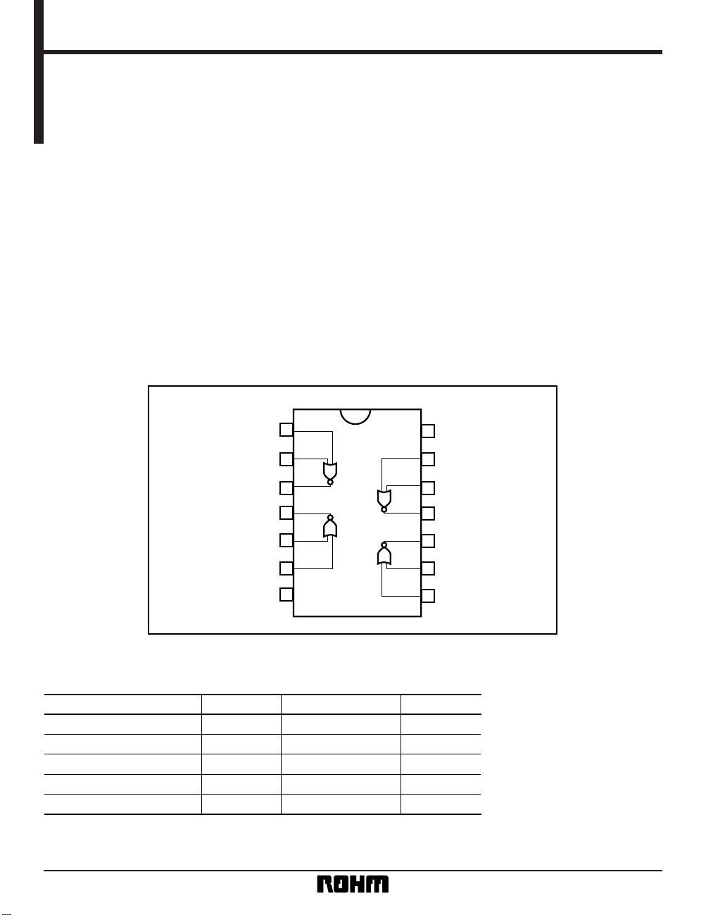
The BU4001B and BU4001BF are 2-input positive logic NOR gates, each with four built-in circuits. A buffer achieved
by an inverter added at the gate output improves the input / output propagation characteristic and minimizes variation
in the propagation time caused by increase of the load capacitance.
•
Block diagram
A1
1
B1
2
O1
3
O2
4
B2
5
A2
6
VSS
7
14
13
12
11
10
9
8
VDD
A4
B4
O4
O3
B3
A3
•
Features
1) Low power dissipation.
2) Wide range of operating power supply voltage.
3) High input impedance.
4) High fan-out.
5) Direct drive of 2 L-TTL inputs and 1 LS-TTL input.
•
Absolute maximum ratings (VSS = 0V, Ta = 25°C)
Parameter Symbol Limits Unit
Power supply voltage V
DD V
Power dissipation mW
Operating temperature Topr
°C
Storage temperature Tstg °C
Input voltage V
IN – 0.3 ~ VDD + 0.3 V
Pd
– 0.3 ~ + 18
– 40 ~ + 85
– 55 ~ + 150
1000 (DIP), 450 (SOP)
Page 2
2
Standard ICs BU4001B / BU4001BF
•
Electrical characteristics
DC characteristics (unless otherwise noted, V
SS = 0V, Ta = 25°C)
Parameter Symbol Min. Typ. Max. Unit Conditions
Measurement
circuit
Input high level voltage V
IH
3.5
——
V
5
—
Fig.17.0
——
10
11.0
——
15
Input low level voltage V
IL
——
1.5
V
5
—
Fig.1
——
3.0 10
——
4.0 15
Input high level current I
IH
—
—
0.3
µ
A15V
IH
=
15V Fig.1
Input low level current I
IL
—
—
–
0.3
µ
A15V
IL
=
0V Fig.1
Output high level voltage V
OH
4.95
——
V
5
IO =
0mA Fig.19.95
——
10
14.95
——
15
Output low level voltage V
OL
—
—
0.05
V
5
I
O
=
0mA Fig.1
—
—
0.05 10
—
—
0.05 15
Output high level current I
OH
–
0.16
——
mA
5V
OH
=
4.6V
Fig.1
–
0.4
——
10 VOH =
9.5V
–
1.2
——
15 VOH =
13.5V
Output low level current I
OL
0.44
—
—
mA
5V
OL
=
0.4V
Fig.11.1
—
—
10 VOL =
0.5V
3.0
—
—
15 VOL =
1.5V
Static current dissipation I
DD
——
1
µ
A
5
VI =
VDD or GND
—
——
210
——
415
VDD (V)
Page 3

3
Standard ICs BU4001B / BU4001BF
Switching characteristics (unless otherwise noted, VSS = 0V, Ta = 25°C, CL = 50pF)
Parameter Symbol Min. Typ. Max. Unit Conditions
Measurement
circuit
t
TLH
—
180
—
ns
5
—
Fig.2
—
90
—
10
—
65
—
15
t
THL
—
100
—
ns
5
—
Fig.2
—
50
—
10
—
40
—
15
t
PLH
—
90
—
ns
5
—
Fig.2
—
50
—
10
—
40
—
15
t
PHL
—
90
—
ns
5
—
Fig.2
—
50
—
10
—
40
—
15
C
IN
—
5
—
pF
—— —
VDD (V)
Propagation delay time,
“L” to “H”
Propagation delay time,
“H” to “L”
Output rise time
Output fall time
Input capacitance
•
Measurement circuits
VDD
V
A
Fig.1 DC characteristics
GND
P.G
VDD
CL = 50pF
90%
50%
10%
90%
50%
10%
t
THL tTLH
Input
Output
20ns
20ns
t
PHL
tPLH
Fig.2 Switching characteristics
GND
•
Electrical characteristic curve
POWER DISSIPATION: Pd (mW)
AMBIENT TEMPERATURE: Ta (°C)
1200
DIP14
1000
800
600
400
200
0
0255075
100 125 150
SOP14
Fig.3 Power dissipation vs. Ta
characteristic
Page 4

4
Standard ICs BU4001B / BU4001BF
•
External dimensions (Units: mm)
DIP14 SOP14
BU4001B BU4001BF
0.4 ± 0.11.27
1
14
8.7 ± 0.2
7
8
4.4 ± 0.2
6.2 ± 0.3
0.11
1.5 ± 0.1
0.15
0.15 ± 0.1
0.3Min.
6.5 ± 0.3
19.4 ± 0.3
0.5 ± 0.1
3.2 ± 0.2
4.25 ± 0.3
14 8
71
0.3 ± 0.1
0.51Min.
7.62
0° ~ 15°
2.54
 Loading...