

Page 1
1
Multimedia ICs
3-channel, 8-bit D / A converter
BU3616K
The BU3616K, a CMOS IC, is a high-speed, low-power-consumption 3-channel 8-bit D / A converter. Its internal reference voltage source eliminates the need for an external reference voltage source.
•
Absolute maximum ratings (Ta = 25°C)
Parameter Symbol Limits Unit
Power supply voltage DV
DD – 0.5 ~ + 7.0 V
V
Analog power supply voltage AV
DD
PD
DVDD –
0.3
~
DVDD +
0.3
mW
Input voltage V
IN – 0.5 ~ DVDD + 0.5 V
Output voltage
Storage temperature
Power dissipation
∗
1
VOUT
Tstg
– 0.5 ~ DV
DD + 0.5
– 55 ~ + 125
500
V
°C
∗
1 Reduced by 5.0mW for each increase in Ta of 1°C over 25°C.
•
Applications
Video CDs, CD-V, CD karaoke
•
Features
1) 8-bit resolution.
2) Current output.
3) Low power consumption (typically 75mW).
4) High-speed operation.
5) Internal reference voltage circuit.
6) TTL input.
•
Recommended operating conditions
Parameter Symbol Min. Typ. Max. Unit Conditions
Power supply voltage DV
DD 4.5 5.5 V
Analog power supply voltage AV
DD 4.5 5.0 5.5 V
Transfer clock width
Transfer clock width, low level
RGB setup time
RGB hold time
Input voltage, low level
Input voltage, high level
Operating temperature
TCK
TCKL
TS
TH
V
IL
VIH
TOPR
58.8 — — ns
5.0
15 — ns
5——ns
10 — — ns
—
— 0.8 V
2.2 — — V
– 10 — 70 °C
—
Page 2
2
Multimedia ICs BU3616K
•
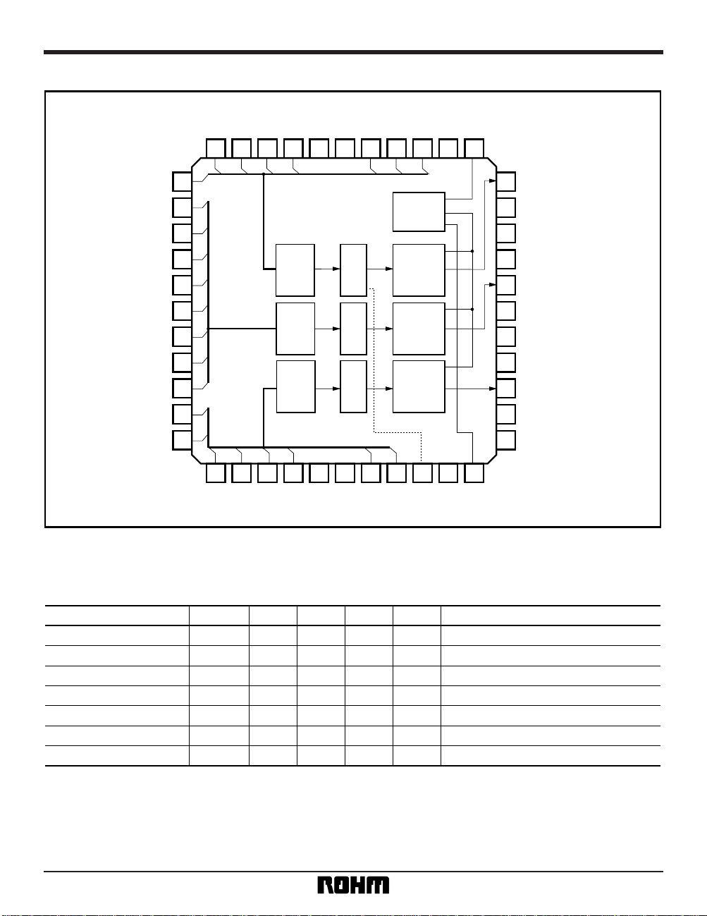
Block diagram
1111098765432
3323 24 25 26 27 28 29 30 31 32
12
13
14
15
16
17
18
19
20
21
22
44
43
R1
R2
R3
R4
DV
DD1
DGND1R5R6
R7
AGND1
Iref
B5
B4
B3
B2
DV
DD2
DGND2
B1
B0
CLK
AV
DD2
Vref
OUTR
AVDDR
AGNDR
N.C.
OUTG
AVDDG
AGNDC
N.C.
OUTB
AVDDB
AGNDB
R0
G7
G6
G5
G4
G3
G2
G1
G0
B7
B6
42
41
40
39
38
37
36
35
34
DECODER
LATCH
CURRENT
CELL
CURRENT
CELL
CURRENT
CELL
LATCH LATCH
DECODER
DECODER
Vref
•
Electrical characteristics (unless otherwise noted, Ta = 25°C, DVDD = 5.0V, AVDD = 5.0V, RREF = 6.8kΩ, RL = 470Ω,
F
CK = 15MHz)
Parameter Symbol Min. Typ. Max. Unit Conditions
Current dissipation I
CC 15 mA
Differential linearity error ED – 0.5 — LSB
Linearity error
Full-scale voltage
RGB output voltage ratio
Output delay time
Settling time
EL
FS
F
SCR
TD
TSET
– 1.0 — LSB
—
1.44 V
DV
DD = 5.0V AVDD = 5.0V
R
REF = 6.8kΩ RL = 470Ω
F
CK = 15MHz
0 0.5 %
—30 ns
1.29
40
30
0.5
1.0
1.58
5.0
—
—ns
C
L = 15pF
C
L = 15pF
—
Page 3

3
Multimedia ICs BU3616K
•
Pin descriptions
Pin No. Pin nameI / O
1 Iref
—
2 AGND 1
—
3R7I
4
5
6
7
8
9
10
11
12
13
14
15
16
17
18
19
20
21
22
23
24
25
26
27
28
29
30
31
32
33
34
35
36
37
R6
R5
DGND1
DV
DD
1
R4
R3
R2
R1
R0
G7
G6
G5
G4
G3
G2
G1
G0
B7
B6
B5
B4
B3
B2
DV
DD
2
DGND2
B1
B0
CLK
AV
DD
2
Vref
AGNDB
AVDDB
OUTB
N.C.
I
I
—
—
I
I
I
I
I
I
I
I
I
I
I
I
I
I
I
I
I
I
I
—
—
I
I
I
—
O
—
—
O
—
Output current adjustment resistor connection, Vref output
Analog ground 1
RED data input (bit 7, MSB)
RED data input (bit 6)
RED data input (bit 5)
Digital ground 1
Digital power supply 1
RED data input (bit 4)
RED data input (bit 3)
RED data input (bit 2)
RED data input (bit 1)
RED data input (bit 0, LSB)
GREEN data input (bit 7, MSB)
GREEN data input (bit 6)
GREEN data input (bit 5)
GREEN data input (bit 4)
GREEN data input (bit 3)
GREEN data input (bit 2)
GREEN data input (bit 1)
GREEN data input (bit 0, LSB)
BLUE data input (bit 7, MSB)
BLUE data input (bit 6)
BLUE data input (bit 5)
BLUE data input (bit 4)
BLUE data input (bit 3)
BLUE data input (bit 2)
Digital power supply 2
Digital ground 2
BLUE data input (bit 1)
BLUE data input (bit 0, LSB)
System lock
Analog power supply 2
Attached capacitance-adding pin (C
=
0.1 µF)
Analog ground B
Analog power supply B
BLUE output
Function
—
Page 4

4
Multimedia ICs BU3616K
•
Input / output circuits
Pin No.
Pin name
Equivalent circuit
3 ~ 5
8 ~ 26
29 ~ 31
R0 ~ R7, G0 ~ G7
B0 ~ B7, CLK
36, 40, 44
OUTR, OUTG
OUTB
1, 33
33
Iref, Vref
1
38
39
40
41
42
43
44
AGNDG
AVDDG
OUTG
N.C.
AGNDR
AVDDR
OUTR
—
—
O
—
—
—
O
Analog ground G
Analog power supply G
GREEN output
Analog ground R
Analog power supply R
RED output
—
Pin No. Pin nameI / O Function
Page 5

5
Multimedia ICs BU3616K
•
Application example
0.1µF
Fig.1
1111098765432
3323 24 25 26 27 28 29 30 31 32
12
13
14
15
16
17
18
19
20
21
22
44
43
R
L
RREF
RED
INPUT
GREEN
INPUT
BLUE
INPUT
CLK
RED
OUTPUT
R
L
GREEN
OUTPUT
R
L
BLUE
OUTPUT
42
41
40
39
38
37
36
35
34
DECODER
LATCH
CURRENT
CELL
CURRENT
CELL
CURRENT
CELL
LATCH LATCH
DECODER
DECODER
Vref
•
External dimensions (Units: mm)
QFP44
33 23
22
12
1
34
44
10.0 ± 0.2
14.0 ± 0.3
0.35 ± 0.1
10.0 ± 0.2
14.0 ± 0.3
1.2
0.05
2.15 ± 0.1
0.15 ± 0.1
0.8
11
0.15
 Loading...