

Page 1
ОООООООО
ÎÎÎÎ
ОООООООО
ÎÎÎÎ
ОООООООО
ÎÎÎÎ
Î
Î
ОООООООО
Î
ÎÎÎÎ
Î
Î
Î
ОООООООО
Î
ÎÎÎÎ
Î
ОООООООО
ÎÎÎÎ
ОООООООО
ÎÎÎÎ
ОООООООО
ÎÎÎÎ
ОООООООО
ÎÎÎÎ
Î
Î
ОООООООО
Î
ÎÎÎÎ
Î
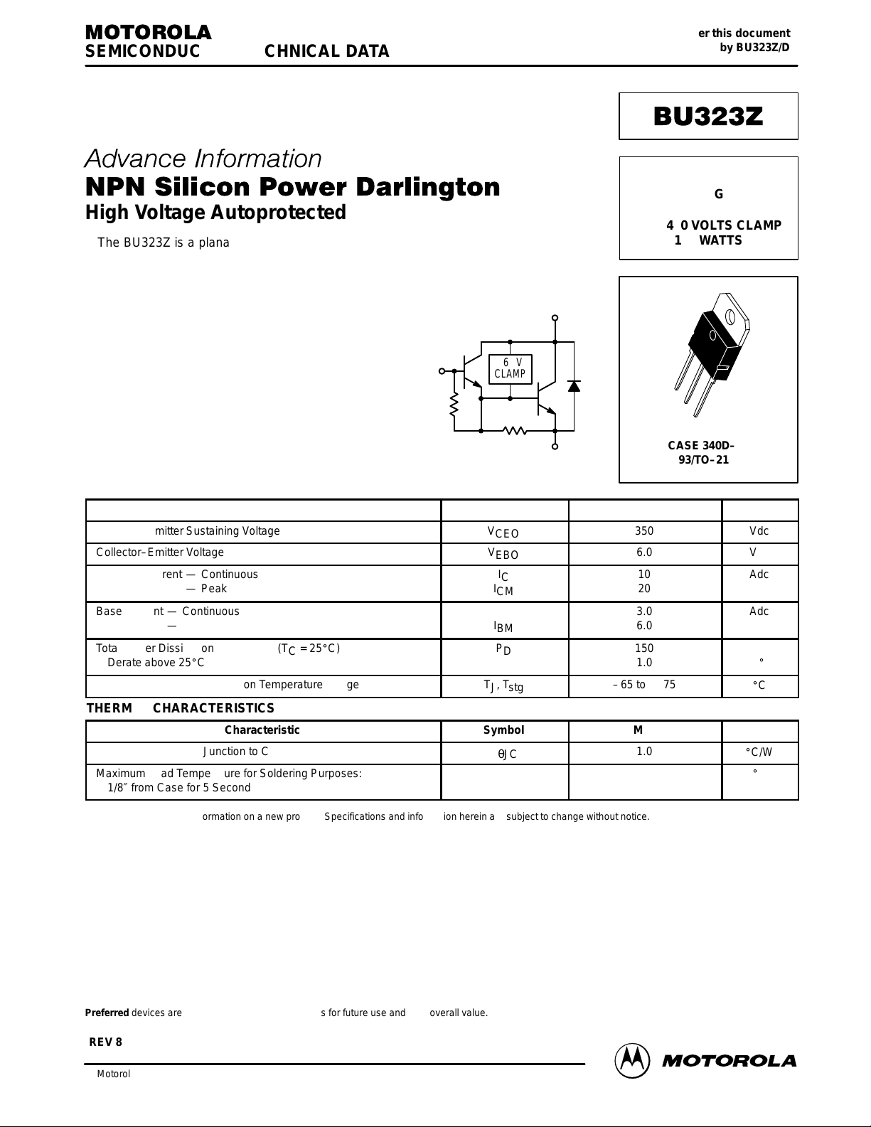
SEMICONDUCTOR TECHNICAL DATA
High Voltage Autoprotected
The BU323Z is a planar, monolithic, high–voltage power Darlington with a built–in
active zener clamping circuit. This device is specifically designed for unclamped,
inductive applications such as Electronic Ignition, Switching Regulators and Motor
Control, and exhibit the following main features:
• Integrated High–Voltage Active Clamp
• Tight Clamping Voltage Window (350 V to 450 V) Guaranteed
Over the –40°C to +125°C Temperature Range
• Clamping Energy Capability 100% Tested in a Live
Ignition Circuit
• High DC Current Gain/Low Saturation Voltages
Specified Over Full Temperature Range
• Design Guarantees Operation in SOA at All Times
• Offered in Plastic SOT–93/TO–218 Type or
TO–220 Packages
360 V
CLAMP
Order this document
by BU323Z/D
AUTOPROTECTED
DARLINGTON
10 AMPERES
360–450 VOLTS CLAMP
150 WATTS
CASE 340D–02
SOT–93/TO–218 TYPE
MAXIMUM RATINGS
Rating
Collector–Emitter Sustaining V oltage
Collector–Emitter Voltage
Collector Current — Continuous
ОООООООООООООООО
— Peak
Base Current — Continuous
ОООООООООООООООО
— Peak
Total Power Dissipation (TC = 25_C)
Derate above 25_C
Operating and Storage Junction Temperature Range
THERMAL CHARACTERISTICS
ОООООООООООООООООООООООООООООООО
ОООООООООООООООО
Thermal Resistance, Junction to Case
ОООООООООООООООО
Maximum Lead Temperature for Soldering Purposes:
ОООООООООООООООО
1/8″ from Case for 5 Seconds
This document contains information on a new product. Specifications and information herein are subject to change without notice.
Characteristic
Symbol
V
CEO
V
EBO
I
C
ООООО
I
CM
I
B
I
BM
ООООО
P
D
TJ, T
stg
Symbol
ООООО
R
θJC
ООООО
T
ООООО
L
Value
350
6.0
ООООООО
10
20
3.0
ООООООО
6.0
150
1.0
–65 to +175
ООООООО
ООООООО
ООООООО
Max
1.0
260
Unit
Vdc
Vdc
Adc
ÎÎÎ
Adc
ÎÎÎ
Watts
W/_C
_
C
Unit
ÎÎÎ
_
C/W
ÎÎÎ
_
C
ÎÎÎ
Preferred devices are Motorola recommended choices for future use and best overall value.
REV 8
Motorola, Inc. 1996
Motorola Bipolar Power Transistor Device Data
1
Page 2
BU323Z
ÎÎÎ
Î
Î
Î
Î
Î
ÎÎÎ
Î
Î
Î
Î
Î
Î
Î
Î
Î
Î
Î
Î
Î
Î
Î
Î
Î
Î
Î
Î
Î
Î
Î
Î
Î
Î
Î
Î
Î
Î
Î
Î
Î
Î
Î
Î
Î
Î
Î
Î
Î
Î
Î
Î
Î
Î
Î
Î
Î
Î
Î
Î
Î
Î
Î
Î
Î
Î
Î
Î
Î
Î
Î
Î
Î
Î
Î
Î
Î
Î
Î
Î
Î
(I
C
I
B1
() ()
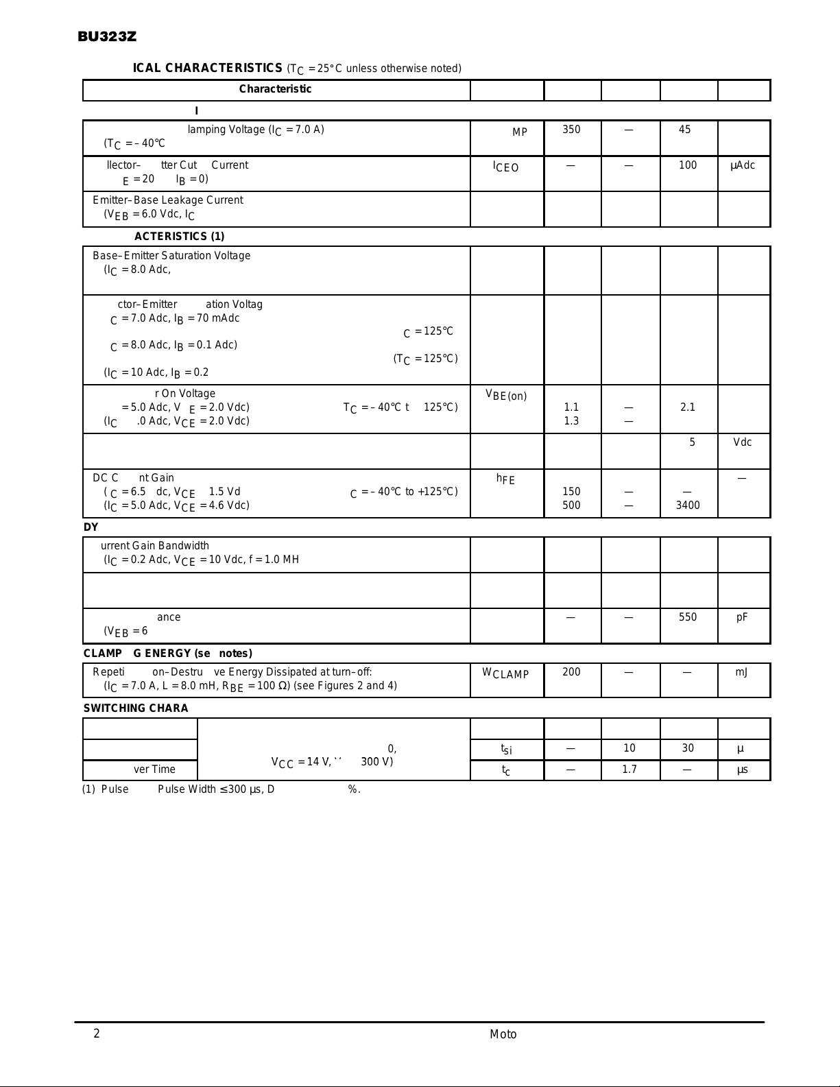
ELECTRICAL CHARACTERISTICS (T
= 25_C unless otherwise noted)
C
Characteristic
OFF CHARACTERISTICS (1)
Collector–Emitter Clamping Voltage (IC = 7.0 A)
(TC = –40°C to +125°C)
ОООООООООООООООООО
Collector–Emitter Cutoff Current
(VCE = 200 V, IB = 0)
ОООООООООООООООООО
Emitter–Base Leakage Current
(VEB = 6.0 Vdc, IC = 0)
ON CHARACTERISTICS (1)
Base–Emitter Saturation Voltage
(IC = 8.0 Adc, IB = 100 mAdc)
ОООООООООООООООООО
(IC = 10 Adc, IB = 0.25 Adc)
ОООООООООООООООООО
Collector–Emitter Saturation Voltage
ОООООООООООООООООО
(IC = 7.0 Adc, IB = 70 mAdc)
ОООООООООООООООООО
(IC = 8.0 Adc, IB = 0.1 Adc)
ОООООООООООООООООО
(IC = 10 Adc, IB = 0.25 Adc)
ОООООООООООООООООО
(TC = 125°C)
(TC = 125°C)
Base–Emitter On Voltage
(IC = 5.0 Adc, VCE = 2.0 Vdc) (TC = –40°C to +125°C)
ОООООООООООООООООО
(IC = 8.0 Adc, VCE = 2.0 Vdc)
Diode Forward Voltage Drop
(IF = 10 Adc)
ОООООООООООООООООО
DC Current Gain
(IC = 6.5 Adc, VCE = 1.5 Vdc) (TC = –40°C to +125°C)
ОООООООООООООООООО
(IC = 5.0 Adc, VCE = 4.6 Vdc)
DYNAMIC CHARACTERISTICS
Current Gain Bandwidth
(IC = 0.2 Adc, VCE = 10 Vdc, f = 1.0 MHz)
ОООООООООООООООООО
Output Capacitance
(VCB = 10 Vdc, IE = 0, f = 1.0 MHz)
Input Capacitance
ОООООООООООООООООО
(VEB = 6.0 V)
CLAMPING ENERGY (see notes)
Repetitive Non–Destructive Energy Dissipated at turn–off:
(IC = 7.0 A, L = 8.0 mH, RBE = 100 Ω) (see Figures 2 and 4)
ОООООООООООООООООО
SWITCHING CHARACTERISTICS: Inductive Load (L = 10 mH)
Fall Time
Storage Time
Cross–over Time
I
= 6.5 A I = 45 mA
= 6.5 A,
V
BE(off)
VCC = 14 V, VZ = 300 V)
= 0, R
= 45 mA,
BE(off)
= 0,
(1) Pulse Test: Pulse Width ≤ 300 µs, Duty Cycle = 2.0%.
Symbol
V
CLAMP
ÎÎ
I
CEO
ÎÎ
I
EBO
V
BE(sat)
ÎÎ
ÎÎ
V
CE(sat)
ÎÎ
ÎÎ
ÎÎ
ÎÎ
V
BE(on)
ÎÎ
V
F
ÎÎ
h
FE
ÎÎ
f
T
ÎÎ
C
ob
C
ib
ÎÎ
W
CLAMP
ÎÎ
t
fi
t
si
t
c
Min
350
ÎÎ
—
ÎÎ
—
—
ÎÎ
—
ÎÎ
ÎÎ
—
—
ÎÎ
—
ÎÎ
—
—
ÎÎ
1.1
ÎÎ
1.3
—
ÎÎ
150
ÎÎ
500
—
ÎÎ
—
—
ÎÎ
200
ÎÎ
—
—
—
Typ
—
ÎÎ
—
ÎÎ
—
—
ÎÎ
—
ÎÎ
ÎÎ
—
—
ÎÎ
—
ÎÎ
—
—
ÎÎ
—
ÎÎ
—
—
ÎÎ
—
ÎÎ
—
—
ÎÎ
—
—
ÎÎ
—
ÎÎ
625
10
1.7
Max
450
ÎÎ
100
ÎÎ
50
2.2
ÎÎ
2.5
ÎÎ
ÎÎ
1.6
1.8
ÎÎ
1.8
ÎÎ
2.1
1.7
ÎÎ
2.1
ÎÎ
2.3
2.5
ÎÎ
—
ÎÎ
3400
2.0
ÎÎ
200
550
ÎÎ
—
ÎÎ
—
30
—
Unit
Vdc
ÎÎ
µAdc
ÎÎ
mAdc
Vdc
ÎÎ
ÎÎ
Vdc
ÎÎ
ÎÎ
ÎÎ
ÎÎ
Vdc
ÎÎ
Vdc
ÎÎ
—
ÎÎ
MHz
ÎÎ
pF
pF
ÎÎ
mJ
ÎÎ
ns
µs
µs
2
Motorola Bipolar Power Transistor Device Data
Page 3

I
= 6.5 A
NOM
Icer Leakage Current
I
C
Output transistor turns on: IC = 40 mA
High Voltage Circuit turns on: IC = 20 mA
µ
Avalanche diode turns on: IC = 100
A
250 V 300 V 340 V
Figure 1. IC = f(VCE) Curve Shape
V
CLAMP
V
CE
NOMINAL
= 400 V
BU323Z
By design, the BU323Z has a built–in avalanche diode and
a special high voltage driving circuit. During an auto–protect
cycle, the transistor is turned on again as soon as a voltage,
determined by the zener threshold and the network, is
reached. This prevents the transistor from going into a
Reverse Bias Operating limit condition. Therefore, the device
will have an extended safe operating area and will always
appear to be in “FBSOA.” Because of the built–in zener and
associated network, the IC = f( VCE) curve exhibits an
unfamiliar shape compared to standard products as shown in
Figure 1.
IB CURRENT
SOURCE
Ω
L INDUCTANCE
(8 mH)
V
CE
MONITOR
(V
)
GATE
I
C
MONITOR
MERCURY CONT ACTS
WETTED RELAY
RBE = 100
V
BEoff
IB2 SOURCE
Figure 2. Basic Energy T est Circuit
10
TC = 25
1
0.1
IC CURRENT
SOURCE
Ω
0.1
NON
INDUCTIVE
°
C
The bias parameters, V
CLAMP
, IB1, V
BE(off)
the inductance, are applied according to the Device Under
Test (DUT) specifications. VCE and IC are monitored by the
test system while making sure the load line remains within
the limits as described in Figure 4.
Note: All BU323Z ignition devices are 100% energy tested,
per the test circuit and criteria described in Figures 2 and 4,
to the minimum guaranteed repetitive energy, as specified in
the device parameter section. The device can sustain this
energy on a repetitive basis without degrading any of the
specified electrical characteristics of the devices. The units
under test are kept functional during the complete test sequence for the test conditions described:
I
C(peak)
RBE= 100 Ω, V
10 ms
250 ms
= 7.0 A, ICH = 5.0 A, ICL = 100 mA, IB = 100 mA,
= 280 V, L = 8.0 mH
gate
300µs
1ms
, IB2, IC, and
0.01
, COLLECTOR CURRENT (AMPS)
C
I
0.001
Figure 3. Forward Bias Safe Operating Area
Motorola Bipolar Power Transistor Device Data
THERMAL LIMIT
SECOND BREAKDOWN LIMIT
CURVES APPLY BELOW
RATED V
CEO
VCE, COLLECTOR–EMITTER VOL TAGE (VOLTS)
1000340 V10010
3
Page 4

BU323Z
I
CPEAK
I
CPEAK
I
C
The shaded area represents the amount of energy the de-
IC HIGH
vice can sustain, under given DC biases (IC/IB/V
RBE), without an external clamp; see the test schematic dia-
BE(off)
/
gram, Figure 2.
The transistor P ASSES the Energy test if, for the inductive
load and I
CPEAK/IB/VBE(off)
the shaded area and greater than the V
IC LOW
V
CE
Figure 4a.
I
C
V
GATE
IC HIGH
IC LOW
MIN
V
CE
Figure 4a.
biases, the VCE remains outside
minimum limit,
GA TE
I
CPEAK
I
CPEAK
Figure 4b.
V
GATE
MIN
The transistor FAILS if the VCE is less than the V
GATE
(minimum limit) at any point along the VCE/IC curve as
I
C
shown on Figures 4b, and 4c. This assures that hot spots
and uncontrolled avalanche are not being generated in the
IC HIGH
IC LOW
V
CE
Figure 4c.
I
C
V
GATE
IC HIGH
MIN
die, and the transistor is not damaged, thus enabling the
sustained energy level required.
The transistor FAILS if its Collector/Emitter breakdown
voltage is less than the V
IC LOW
value, Figure 4d.
GATE
V
CE
Figure 4d.
V
GATE
MIN
Figure 4. Energy Test Criteria for BU323Z
4
Motorola Bipolar Power Transistor Device Data
Page 5

BU323Z
10000
1000
, DC CURRENT GAIN
100
FE
h
5.0
4.5
4.0
3.5
3.0
2.5
2.0
1.5
1.0
, COLLECTOR–EMITTER VOL TAGE (VOLTS)
0.5
CE
V
10
10000
TYPICAL
°
C
TJ = 125
1000
TYP – 6
–40°C
25°C
VCE = 1.5 V
100001000100
IC, COLLECTOR CURRENT (MILLIAMPS)
, DC CURRENT GAIN
FE
h
Figure 5. DC Current Gain
TJ = 25
°
IC = 3 A
5 A
0
IB, BASE CURRENT (MILLIAMPS)
8 A
10 A
7 A
C
, COLLECTOR–EMITTER VOL TAGE (VOLTS)
CE
100101
V
100
10
2.4
2.2
2.0
1.8
1.6
1.4
1.2
1.0
0.8
0.6
0.4
TYP + 6
Σ
VCE = 5 V, TJ = 25°C
IC, COLLECTOR CURRENT (MILLIAMPS)
Figure 6. DC Current Gain
IC/IB = 150
25°C
IC, COLLECTOR CURRENT (AMPS)
Σ
10000
1000001000100
TJ = 125°C
1010.1
, BASE–EMITTER VOLTAGE (VOLTS)
BE
V
Figure 7. Collector Saturation Region
2.0
1.8
1.6
1.4
1.2
1.0
0.8
IC/IB = 150
TJ = 25°C
IC, COLLECTOR CURRENT (AMPS)
Figure 9. Base–Emitter Saturation V oltage
125°C
Figure 8. Collector–Emitter Saturation V oltage
2.0
VCE = 2 VOLTS
1.8
1.6
1.4
1.2
1.0
, BASE–EMITTER VOLTAGE (VOLTS)
0.8
BE(on)
V
1010.1
0.6
TJ = 25°C
125°C
1010.1
IC, COLLECTOR CURRENT (AMPS)
Figure 10. Base–Emitter “ON” Voltages
Motorola Bipolar Power Transistor Device Data
5
Page 6

BU323Z
P ACKAGE DIMENSIONS
C
B
U
L
S
K
4
123
Q
E
A
D
J
H
V
G
NOTES:
1. DIMENSIONING AND TOLERANCING PER ANSI
Y14.5M, 1982.
2. CONTROLLING DIMENSION: MILLIMETER.
DIM MIN MAX MIN MAX
A ––– 20.35 ––– 0.801
B 14.70 15.20 0.579 0.598
C 4.70 4.90 0.185 0.193
D 1.10 1.30 0.043 0.051
E 1.17 1.37 0.046 0.054
G 5.40 5.55 0.213 0.219
H 2.00 3.00 0.079 0.118
J 0.50 0.78 0.020 0.031
K 31.00 REF 1.220 REF
L ––– 16.20 ––– 0.638
Q 4.00 4.10 0.158 0.161
S 17.80 18.20 0.701 0.717
U 4.00 REF 0.157 REF
V 1.75 REF 0.069
STYLE 1:
PIN 1. BASE
2. COLLECTOR
3. EMITTER
4. COLLECTOR
INCHESMILLIMETERS
CASE 340D–02
SOT–93/TO–218 TYPE
ISSUE B
Motorola reserves the right to make changes without further notice to any products herein. Motorola makes no warranty , representation or guarantee regarding
the suitability of its products for any particular purpose, nor does Motorola assume any liability arising out of the application or use of any product or circuit, and
specifically disclaims any and all liability, including without limitation consequential or incidental damages. “T ypical” parameters which may be provided in Motorola
data sheets and/or specifications can and do vary in different applications and actual performance may vary over time. All operating parameters, including “Typicals”
must be validated for each customer application by customer’s technical experts. Motorola does not convey any license under its patent rights nor the rights of
others. Motorola products are not designed, intended, or authorized for use as components in systems intended for surgical implant into the body, or other
applications intended to support or sustain life, or for any other application in which the failure of the Motorola product could create a situation where personal injury
or death may occur. Should Buyer purchase or use Motorola products for any such unintended or unauthorized application, Buyer shall indemnify and hold Motorola
and its officers, employees, subsidiaries, affiliates, and distributors harmless against all claims, costs, damages, and expenses, and reasonable attorney fees
arising out of, directly or indirectly, any claim of personal injury or death associated with such unintended or unauthorized use, even if such claim alleges that
Motorola was negligent regarding the design or manufacture of the part. Motorola and are registered trademarks of Motorola, Inc. Motorola, Inc. is an Equal
Opportunity/Affirmative Action Employer.
How to reach us:
USA/EUROPE/Locations Not Listed: Motorola Literature Distribution; JAPAN: Nippon Motorola Ltd.; Tatsumi–SPD–JLDC, 6F Seibu–Butsuryu–Center,
P.O. Box 20912; Phoenix, Arizona 85036. 1–800–441–2447 or 602–303–5454 3–14–2 T atsumi Koto–Ku, Tokyo 135, Japan. 03–81–3521–8315
MFAX: RMF AX0@email.sps.mot.com – TOUCHT ONE 602–244–6609 ASIA/PACIFIC: Motorola Semiconductors H.K. Ltd.; 8B Tai Ping Industrial Park,
INTERNET: http://Design–NET.com 51 Ting Kok Road, Tai Po, N.T., Hong Kong. 852–26629298
6
◊
Motorola Bipolar Power Transistor Device Data
BU323Z/D
*BU323Z/D*
 Loading...