

Page 1

现货库存、技术资料、百科信息、热点资讯,精彩尽在鼎好!
Data Sheet, Rev. 2.0, May 2006
BTS 7970B
High Current PN Half Bridge
TM
NovalithIC
68 A, 7 mΩ + 9 mΩ typ.
Automotive Power
Never stop thinking.
Page 2

High Current PN Half Bridge
BTS 7970B
Product Summary . . . . . . . . . . . . . . . . . . . . . . . . . . . . . . . . . . . . . . . . . . . . . . . . . . . .2
Basic Features . . . . . . . . . . . . . . . . . . . . . . . . . . . . . . . . . . . . . . . . . . . . . . . . . . . . . . .2
1Overview . . . . . . . . . . . . . . . . . . . . . . . . . . . . . . . . . . . . . . . . . . . . . . . . . . . . . . . . .3
1.1 Block Diagram . . . . . . . . . . . . . . . . . . . . . . . . . . . . . . . . . . . . . . . . . . . . . . . . . . .3
1.2 Terms . . . . . . . . . . . . . . . . . . . . . . . . . . . . . . . . . . . . . . . . . . . . . . . . . . . . . . . . .4
2 Pin Configuration . . . . . . . . . . . . . . . . . . . . . . . . . . . . . . . . . . . . . . . . . . . . . . . . . .5
2.1 Pin Assignment . . . . . . . . . . . . . . . . . . . . . . . . . . . . . . . . . . . . . . . . . . . . . . . . . .5
2.2 Pin Definitions and Functions . . . . . . . . . . . . . . . . . . . . . . . . . . . . . . . . . . . . . . .5
3 Maximum Ratings . . . . . . . . . . . . . . . . . . . . . . . . . . . . . . . . . . . . . . . . . . . . . . . . . .6
Maximum Single Pulse Current . . . . . . . . . . . . . . . . . . . . . . . . . . . . . . . . . . . . . . . . .7
1 Block Description and Characteristics . . . . . . . . . . . . . . . . . . . . . . . . . . . . . . . . .8
1.1 Supply Characteristics . . . . . . . . . . . . . . . . . . . . . . . . . . . . . . . . . . . . . . . . . . . . .8
1.2 Power Stages . . . . . . . . . . . . . . . . . . . . . . . . . . . . . . . . . . . . . . . . . . . . . . . . . . .9
1.2.1 Power Stages - Static Characteristics . . . . . . . . . . . . . . . . . . . . . . . . . . . 10
1.2.2 Switching Times . . . . . . . . . . . . . . . . . . . . . . . . . . . . . . . . . . . . . . . . . . . 11
1.2.3 Power Stages - Dynamic Characteristics . . . . . . . . . . . . . . . . . . . . . . . . 12
1.3 Protection Functions . . . . . . . . . . . . . . . . . . . . . . . . . . . . . . . . . . . . . . . . . . . . .14
1.3.1 Overvoltage Lock Out . . . . . . . . . . . . . . . . . . . . . . . . . . . . . . . . . . . . . . . 14
1.3.2 Undervoltage Shut Down . . . . . . . . . . . . . . . . . . . . . . . . . . . . . . . . . . . . . 14
1.3.3 Overtemperature Protection . . . . . . . . . . . . . . . . . . . . . . . . . . . . . . . . . . 14
1.3.4 Current Limitation . . . . . . . . . . . . . . . . . . . . . . . . . . . . . . . . . . . . . . . . . . 14
1.3.5 Short Circuit Protection . . . . . . . . . . . . . . . . . . . . . . . . . . . . . . . . . . . . . . 16
1.3.6 Electrical Characteristics - Protection Functions . . . . . . . . . . . . . . . . . . . 17
1.4 Control and Diagnostics . . . . . . . . . . . . . . . . . . . . . . . . . . . . . . . . . . . . . . . . . .18
1.4.1 Input Circuit . . . . . . . . . . . . . . . . . . . . . . . . . . . . . . . . . . . . . . . . . . . . . . . 18
1.4.2 Dead Time Generation . . . . . . . . . . . . . . . . . . . . . . . . . . . . . . . . . . . . . . 18
1.4.3 Adjustable Slew Rate . . . . . . . . . . . . . . . . . . . . . . . . . . . . . . . . . . . . . . . 18
1.4.4 Status Flag Diagnosis With Current Sense Capability . . . . . . . . . . . . . . 18
1.4.5 Truth Table . . . . . . . . . . . . . . . . . . . . . . . . . . . . . . . . . . . . . . . . . . . . . . . 20
1.4.6 Electrical Characteristics - Control and Diagnostics . . . . . . . . . . . . . . . . 21
2 Thermal Characteristics . . . . . . . . . . . . . . . . . . . . . . . . . . . . . . . . . . . . . . . . . . . .22
3 Application . . . . . . . . . . . . . . . . . . . . . . . . . . . . . . . . . . . . . . . . . . . . . . . . . . . . . . .23
3.1 Application Example . . . . . . . . . . . . . . . . . . . . . . . . . . . . . . . . . . . . . . . . . . . . .23
3.2 Layout Considerations . . . . . . . . . . . . . . . . . . . . . . . . . . . . . . . . . . . . . . . . . . . .23
4 Package Outlines P-TO-263-7 . . . . . . . . . . . . . . . . . . . . . . . . . . . . . . . . . . . . . . .24
5 Revision History . . . . . . . . . . . . . . . . . . . . . . . . . . . . . . . . . . . . . . . . . . . . . . . . . .25
Data Sheet 1 Rev. 2.0, 2006-05-09
Page 3

High Current PN Half Bridge
NovalithIC
TM
BTS 7970B
Product Summary
The BTS 7970B is a fully integrated high current half
bridge for motor drive applications. It is part of the
NovalithICTM family containing one p-channel highside
MOSFET and one n-channel lowside MOSFET with an
integrated driver IC in one package. Due to the p-channel
highside switch the need for a charge pump is eliminated
thus minimizing EMI. Interfacing to a microcontroller is
made easy by the integrated driver IC which features
logic level inputs, diagnosis with current sense, slew rate
adjustment, dead time generation and protection against overtemperature, overvoltage,
undervoltage, overcurrent and short circuit.
The BTS 7970B provides a cost optimized solution for protected high current PWM
motor drives with very low board space consumption.
BTS 7970B
P-TO-263-7
Basic Features
• Path resistance of typ. 16 mΩ @25°C
• Low quiescent current of typ. 7 µA @ 25 °C
• PWM capability of up to 25 kHz combined with active freewheeling
• Switched mode current limitation for reduced power dissipation in overcurrent
• Current limitation level of 68 A typ. / 50 A min.
• Status flag diagnosis with current sense capability
• Overtemperature shut down with latch behaviour
• Overvoltage lock out
• Undervoltage shut down
• Driver circuit with logic level inputs
• Adjustable slew rates for optimized EMI
Type Package
BTS 7970B P-TO-263-7
Data Sheet 2 Rev. 2.0, 2006-05-09
Page 4
High Current PN Half Bridge
BTS 7970B
Overview
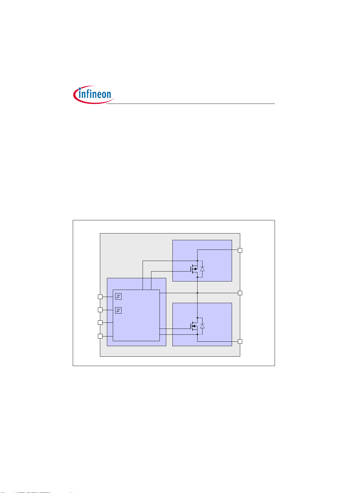
1Overview
The BTS 7970B is part of the NovalithIC family containing three separate chips in one
package: One p-channel highside MOSFET and one n-channel lowside MOSFET
together with a driver IC, forming a fully integrated high current half-bridge. All three
chips are mounted on one common leadframe, using the chip on chip and chip by chip
technology. The power switches utilize vertical MOS technologies to ensure optimum on
state resistance. Due to the p-channel highside switch the need for a charge pump is
eliminated thus minimizing EMI. Interfacing to a microcontroller is made easy by the
integrated driver IC which features logic level inputs, diagnosis with current sense, slew
rate adjustment, dead time generation and protection against overtemperature,
overvoltage, undervoltage, overcurrent and short circuit. The BTS 7970B can be
combined with other BTS 7970B to form H-bridge and 3-phase drive configurations.
1.1 Block Diagram
BTS 7970B
HS base-chip
VS
Top-chip
IN
INH
SR
IS
Gate Driver
Dead Time Gen.
Slew Rate Adj.
UV Shut Down
OV Lock Out
OT Shut Dow n
Current Lim.
Diagnosis
Current Sense
LS bas e-c hip
OUT
GND
Figure 1 Block Diagram
Data Sheet 3 Rev. 2.0, 2006-05-09
Page 5

High Current PN Half Bridge
BTS 7970B
1.2 Terms
Following figure shows the terms used in this data sheet.
V
VS ,VS
I
IN
V
IN
I
INH
V
INH
I
SR
V
SR
I
IS
V
IS
Figure 2 Terms
IN
INH
BTS 7970B
SR
IS
VS
GND
I
IVS, -I
D(HS)
GND,ID(LS)
OUT
I
OUT
V
SD (L S)
V
DS(HS)
, I
L
Overview
V
OUT
Data Sheet 4 Rev. 2.0, 2006-05-09
Page 6

High Current PN Half Bridge
BTS 7970B
2 Pin Configuration
2.1 Pin Assignment
BTS 7970B
P-TO-263-7
8
123567
4
Figure 3 Pin Assignment BTS 7970B and (top view)
Pin Configuration
2.2 Pin Definitions and Functions
Pin Symbol I/O Function
1 GND - Ground
2 IN I Input
Defines whether high- or lowside switch is activated
3 INH I Inhibit
When set to low device goes in sleep mode
4,8 OUT O Power output of the bridge
5 SR I Slew Rate
The slew rate of the power switches can be adjusted
by connecting a resistor between SR and GND
6 IS O Current Sense and Diagnosis
7 VS - Supply
Bold type: Pin needs power wiring
Data Sheet 5 Rev. 2.0, 2006-05-09
Page 7

High Current PN Half Bridge
BTS 7970B
Maximum Ratings
3 Maximum Ratings
-40 °C < Tj < 150 °C (unless otherwise specified)
Pos Parameter Symbol Limits Unit Test Condition
min max
Electrical Maximum Ratings
3.0.1 Supply voltage
3.0.2 Logic Input Voltage
3.0.3 HS/LS continuous drain
current
3.0.4 HS pulsed drain current I
3.0.5 LS pulsed drain current I
3.0.6 PWM current I
3.0.7 Voltage at SR pin
3.0.8 Voltage between VS and
IS pin
3.0.9 Voltage at IS pin V
Thermal Maximum Ratings
3.0.10 Junction temperature
3.0.11 Storage temperature
ESD Susceptibility
3.0.12 ESD susceptibility
V
VS
V
IN
V
INH
I
D(HS)
I
D(LS)
D(HS)
D(LS)
OUT
V
SR
V
VS -VIS
IS
T
j
T
stg
V
ESD
-0.3 45 V
-0.3 5.3 V
-44 44
1)
A TC < 85°C
switch active
-90 901)A TC < 85°C
= 10ms
t
pulse
-90 901)A
1)
-55 55 A f = 1kHz, DC = 50%
single pulse
-60 60 A f = 20kHz, DC = 50%
-0.3 1.0 V
-0.3 45 V
-20 45 V
-40 150 °C
-55 150 °C
kV HBM
2)
IN, INH, SR, IS
OUT, GND, VS
1)
Maximum reachable current may be smaller depending on current limitation level
2)
ESD susceptibility HBM according to EIA/JESD 22-A 114B
-2
-6
2
6
Note: Maximum ratings are absolute ratings; exceeding any one of these values may
cause irreversible damage to the device. Exposure to maximum rating conditions
for extended periods of time may affect device reliability
Data Sheet 6 Rev. 2.0, 2006-05-09
Page 8

High Current PN Half Bridge
BTS 7970B
Maximum Single Pulse Current
100
90
80
70
60
[A]
50
max
I
40
30
20
10
0
1,0E-03 1,0E-02 1,0E-01 1,0E+00 1,0E+01
t
pulse
Maximum Ratings
[s]
Figure 4 BTS 7970B Maximum Single Pulse Current
This diagram shows the maximum single pulse current that can be driven for a given
t
pulse time
. The maximum reachable current may be smaller depending on the
pulse
current limitation level. Pulse time may be limited due to thermal protection of the device.
Data Sheet 7 Rev. 2.0, 2006-05-09
Page 9

High Current PN Half Bridge
BTS 7970B
Block Description and Characteristics
4 Block Description and Characteristics
4.1 Supply Characteristics
T
– 40 °C <
Pos. Parameter Symbol Limit Values Unit Test Conditions
General
4.1.1 Operating Voltage
4.1.2 Supply Current
4.1.3 Quiescent Current I
< 150 °C, 8 V < VS < 18 V, IL = 0A (unless otherwise specified)
j
min. typ. max.
V
S
I
VS(on)
5.5 – 28 V VS increasing
–23mAV
= 5 V
INH
V
= 0 V or 5 V
IN
R
=0 Ω
SR
DC-mode
normal operation
(no fault condition)
VS(off)
–715µAV
––65µA
= 0 V
INH
V
= 0 V or 5 V
IN
T
<85 °C
j
V
= 0 V
INH
V
= 0 V or 5 V
IN
25
[A]
20
VS(of f)
I
15
10
5
0
-40 0 40 80 120 160
[°C]
T
Figure 5 Quiescent Current (typ.) vs. Junction Temperature
Data Sheet 8 Rev. 2.0, 2006-05-09
Page 10

High Current PN Half Bridge
BTS 7970B
Block Description and Characteristics
4.2 Power Stages
The power stages of the BTS 7970B consist of a p-channel vertical DMOS transistor for
the high side switch and a n-channel vertical DMOS transistor for the low side switch. All
protection and diagnostic functions are located in a separate top chip. Both switches can
be operated up to 25 kHz, allowing active freewheeling and thus minimizing power
dissipation in the forward operation of the integrated diodes.
R
The on state resistance
junction temperature
Figure 6.
High Side Switc h
25
mΩ
20
R
ON(HS)
15
10
5
4 8 12 16 20 24 28
is dependent on the supply voltage VS as well as on the
ON
T
. The typical on state resistance characteristics are shown in
j
Low Side Switc h
25
mΩ
20
R
ON(LS)
= 150°C
T
j
= 25° C
T
j
T
= -40°C
j
V
15
10
V
S
5
4 8 12 16 20 24 28
Tj = 150°C
Tj = 25° C
Tj = -40°C
V
S
V
Figure 6 Typical On State Resistance vs. Supply Voltage
Data Sheet 9 Rev. 2.0, 2006-05-09
Page 11

High Current PN Half Bridge
BTS 7970B
Block Description and Characteristics
4.2.1 Power Stages - Static Characteristics
– 40 °C < Tj < 150 °C, 8 V < VS < 18 V (unless otherwise specified)
Pos. Parameter Symbol Limit Values Unit Test Conditions
min. typ. max.
High Side Switch - Static Characteristics
4.2.1 On state high side
resistance
4.2.2 Leakage current high
side
4.2.3 Reverse diode
forward-voltage high
1)
side
Low Side Switch - Static Characteristics
4.2.4 On state low side
resistance
4.2.5 Leakage current low
side
4.2.6 Reverse diode
forward-voltage low
1)
side
1)
Due to active freewheeling, diode is conducting only for a few µs, depending on R
R
ON(HS)
I
L(LKHS)
V
DS(HS)
R
ON(LS)
I
L(LKLS)
V
SD(LS)
mΩ I
–
7
–
10912.5
––1µAV
– – 50 µA
V
–
0.9
1.5
–
0.8
1.1
–
0.6
0.8
mΩ I
–
91412
–
18
––1µAV
– – 15 µA
V
–
0.9
1.5
–
0.8
1.1
–
0.6
0.8
SR
= 20 A
OUT
V
= 13.5 V
S
T
= 25 °C
j
T
= 150 °C
j
= 0 V
INH
V
= 0 V
OUT
T
< 85 °C
j
V
= 0 V
INH
V
= 0 V
OUT
T
= 150 °C
j
I
=-9A
OUT
T
= -40 °C
j
T
= 25 °C
j
T
= 150 °C
j
=-20A
OUT
V
= 13.5V
S
T
= 25 °C
j
T
= 150 °C
j
= 0 V
INH
V
= V
OUT
T
< 85 °C
j
V
= 0 V
INH
V
= V
OUT
T
= 150 °C
j
I
= 9 A
OUT
T
= -40 °C
j
T
= 25 °C
j
T
= 150 °C
j
S
S
Data Sheet 10 Rev. 2.0, 2006-05-09
Page 12

High Current PN Half Bridge
BTS 7970B
Block Description and Characteristics
4.2.2 Switching Times
IN
t
V
OUT
90%
10%
Figure 7 Definition of switching times high side (R
IN
V
OUT
90%
dr(HS)tr(HS)
t
df( LS)tf(LS)
∆V
OUT
t
df(H S)tf(HS)
∆V
OUT
to GND)
load
t
dr(LS)tr(LS)
t
90%
10%
t
t
90%
10%
∆V
OUT
∆V
OUT
10%
t
Figure 8 Definition of switching times low side (R
load
to VS)
Due to the timing differences for the rising and the falling edge there will be a slight
difference between the length of the input pulse and the length of the output pulse. It can
be calculated using the following formulas:
•
∆
t
= (t
HS
•
∆
t
= (t
LS
Data Sheet 11 Rev. 2.0, 2006-05-09
dr(HS)
df(LS)
+ 0.5 t
+ 0.5 t
r(HS)
f(LS)
) - (t
) - (t
df(HS)
dr(LS)
+ 0.5 t
+ 0.5 t
f(HS)
r(LS)
)
).
Page 13

High Current PN Half Bridge
BTS 7970B
Block Description and Characteristics
4.2.3 Power Stages - Dynamic Characteristics
-40 °C < Tj < 150 °C, VS = 13.5 V, R
Pos. Parameter Symbol Limit Values Unit Test Conditions
HIgh Side Switch Dynamic Characteristics
4.2.7 Rise-time of HS
4.2.8 Slew rate HS on
4.2.9 Switch on delay time
t
r(HS)
∆V
t
r( HS)
t
dr(HS)
HS
4.2.10 Fall-time of HS
4.2.11 Slew rate HS off
4.2.12 Switch off delay time
t
f(HS)
-∆V
t
f(HS)
t
df(HS)
HS
= 2Ω (unless otherwise specified)
load
min. typ. max.
OUT
OUT
0.5
/
1.7
5.6
0.5
/
1.2
1
1.5
–
2
–
2
6
11
–
11
–
–
6
–
–
1.6
3.1
–
4.4
–
2
–
–
–
1.6
2.4
–
3.4
4
14
1
2
6
11
6
10
–
4.3
–
22.4
1.5
–
11
–
–
–
3.2
–
16
µs
V/µs
µs
µs
V/µs
µs
R
SR
R
SR
R
SR
R
SR
R
SR
R
SR
R
SR
R
SR
R
SR
R
SR
R
SR
R
SR
R
SR
R
SR
R
SR
R
SR
R
SR
R
SR
= 0 Ω
= 5.1 kΩ
= 51 kΩ
= 0 Ω
= 5.1 kΩ
= 51 kΩ
= 0 Ω
= 5.1 kΩ
= 51 kΩ
= 0 Ω
= 5.1 kΩ
= 51 kΩ
= 0 Ω
= 5.1 kΩ
= 51 kΩ
= 0 Ω
= 5.1 kΩ
= 51 kΩ
Data Sheet 12 Rev. 2.0, 2006-05-09
Page 14

High Current PN Half Bridge
BTS 7970B
-40 °C <
T
< 150 °C, VS = 13.5 V, R
j
load
Block Description and Characteristics
= 2Ω (unless otherwise specified)
Pos. Parameter Symbol Limit Values Unit Test Conditions
min. typ. max.
Low Side Switch Dynamic Characteristics
1.5
–
11
–
–
–
1.9
–
11
1.5
–
11
–
–
–
5.0
–
25.4
µs
V/µs
µs
µs
V/µs
µs
R
SR
R
SR
R
SR
R
SR
R
SR
R
SR
R
SR
R
SR
R
SR
R
SR
R
SR
R
SR
R
SR
R
SR
R
SR
R
SR
R
SR
R
SR
= 0 Ω
= 5.1 kΩ
= 51 kΩ
= 0 Ω
= 5.1 kΩ
= 51 kΩ
= 0 Ω
= 5.1 kΩ
= 51 kΩ
= 0 Ω
= 5.1 kΩ
= 51 kΩ
= 0 Ω
= 5.1 kΩ
= 51 kΩ
= 0 Ω
= 5.1 kΩ
= 51 kΩ
4.2.13 Rise-time of LS
4.2.14 Slew rate LS switch off
4.2.15 Switch off delay time
LS
4.2.16 Fall-time of LS
4.2.17 Slew rate LS switch on
4.2.18 Switch on delay time
LS
t
r(LS)
∆V
t
r(LS)
t
dr(LS)
t
f(LS)
-∆V
t
f(LS)
t
df(LS)
OUT
OUT
0.5
1
–
2
2
6
/
–
11
–
6
–
1.6
0.6
1.3
–
2.2
2.6
0.5
7
1
–
2
2
6
/
–
11
–
6
–
1.6
2.3
3.6
–
5.6
6.4
16
Data Sheet 13 Rev. 2.0, 2006-05-09
Page 15

High Current PN Half Bridge
BTS 7970B
Block Description and Characteristics
4.3 Protection Functions
The device provides integrated protection functions. These are designed to prevent IC
destruction under fault conditions described in the data sheet. Fault conditions are
considered as “outside” normal operating range. Protection functions are not to be used
for continuous or repetitive operation, with the exception of the current limitation
(Chapter 4.3.4). In a fault condition the BTS 7970B will apply the highest slew rate
possible independent of the connected slew rate resistor. Overvoltage, overtemperature
and overcurrent are indicated by a fault current I
at the IS pin as described in the
IS(LIM)
paragraph “Status Flag Diagnosis With Current Sense Capability” on Page 18 and
Figure 12.
In the following the protection functions are listed in order of their priority. Overvoltage
lock out overrides all other error modes.
4.3.1 Overvoltage Lock Out
To assure a high immunity against overvoltages (e.g. load dump conditions) the device
shuts the lowside MOSFET off and turns the highside MOSFET on, if the supply voltage
is exceeding the over voltage protection level
again with a hysteresis
voltage
V
. In H-bridge configuration, this behavior of the BTS 7970B will lead to
OV(ON)
V
OV(HY)
if the supply voltage decreases below the switch-on
V
. The IC operates in normal mode
OV(OFF)
freewheeling in highside during over voltage.
4.3.2 Undervoltage Shut Down
To avoid uncontrolled motion of the driven motor at low voltages the device shuts off
(output is tri-state), if the supply voltage drops below the switch-off voltage
IC becomes active again with a hysteresis
switch-on voltage
V
UV(ON)
.
V
UV(HY)
if the supply voltage rises above the
V
UV(OFF)
. The
4.3.3 Overtemperature Protection
The BTS 7970B is protected against overtemperature by an integrated temperature
sensor. Overtemperature leads to a shut down of both output stages. This state is
t
latched until the device is reset by a low signal with a minimum length of
pin, provided that its temperature has decreased at least the thermal hysteresis ∆
reset
at the INH
T in the
meantime.
Repetitive use of the overtemperature protection might reduce lifetime.
4.3.4 Current Limitation
The current in the bridge is measured in both switches. As soon as the current in forward
I
direction in one switch (high side or low side) is reaching the limit
deactivated and the other switch is activated for
Data Sheet 14 Rev. 2.0, 2006-05-09
t
. During that time all changes at the
CLS
, this switch is
CLx
Page 16

High Current PN Half Bridge
BTS 7970B
Block Description and Characteristics
IN pin are ignored. However, the INH pin can still be used to switch both MOSFETs off.
After t
after 2 *
the switches return to their initial setting. The error signal at the IS pin is reset
CLS
t
. Unintentional triggering of the current limitation by short current spikes
CLS
(e.g. inflicted by EMI coming from the motor) is suppressed by internal filter circuitry. Due
to thresholds and reaction delay times of the filter circuitry the effective current limitation
I
level
depends on the slew rate of the load current dI/dt as shown in Figure 10
CLx
I
I
I
CLx0
L
CLx
t
CLS
t
Figure 9 Timing Diagram Current Limitation (Inductive Load)
Low SideSwitchHigh Side Switch
90
85
[A]
80
CLH
I
70
65
60
50
I
CLH0
75
55
0 500 1000 1500 2000
Tj = -40° C
Tj = 25° C
T
= 150°C
j
dIL/dt
[A/ms]
90
[A]
80
CLL
I
I
CLL0
= - 40°C
T
70
60
50
0 500 1000 1500 2000
j
Tj = 25°C
Tj = 150°C
dIL/dt
[A/ms]
Figure 10 Current Limitation Level vs. Current Slew Rate dI/dt
Data Sheet 15 Rev. 2.0, 2006-05-09
Page 17

High Current PN Half Bridge
BTS 7970B
High Side Switch
80
A
75
I
CLH
70
65
60
6 8 10 12 14 16 18 2 0
Tj = -40°C
Tj = 25° C
Tj = 150°C
V
V
S
Block Description and Characteristics
Low Side Switch
80
A
75
I
CLL
70
65
60
6 8 10 12 14 16 18 2 0
Tj = -40°C
Tj = 25°C
Tj = 150°C
V
V
S
Figure 11 Typical Current Limitation Detection Levels vs. Supply Voltage
In combination with a typical inductive load, such as a motor, this results in a switched
mode current limitation. That way of limiting the current has the advantage that the power
dissipation in the BTS 7970B is much smaller than by driving the MOSFETs in linear
mode. Therefore it is possible to use the current limitation for a short time without
exceeding the maximum allowed junction temperature (e.g. for limiting the inrush current
during motor start up). However, the regular use of the current limitation is allowed only
as long as the specified maximum junction temperature is not exceeded. Exceeding this
temperature can reduce the lifetime of the device.
4.3.5 Short Circuit Protection
The device is short circuit protected against
• output short circuit to ground
• output short circuit to supply voltage
• short circuit of load
The short circuit protection is realized by the previously described current limitation in
combination with the over-temperature shut down of the device.
Please note: Due to the higher priority of the overvoltage protection the short circuit
protection is inactive in overvoltage conditions.
Data Sheet 16 Rev. 2.0, 2006-05-09
Page 18

High Current PN Half Bridge
BTS 7970B
Block Description and Characteristics
4.3.6 Electrical Characteristics - Protection Functions
– 40 °C < Tj < 150 °C; 8 V < VS < 18 V (unless otherwise specified)
Pos. Parameter Symbol Limit Values Unit Test Conditions
min. typ. max.
Under Voltage Shut Down
4.3.1 Switch-ON voltage
4.3.2 Switch-OFF voltage
4.3.3 ON/OFF hysteresis V
Over Voltage Lock Out
4.3.4 Switch-ON voltage
4.3.5 Switch-OFF voltage
4.3.6 ON/OFF hysteresis
Current Limitation
4.3.7 Current limitation
detection level high
side
4.3.8 Current limitation
detection level low
side
Current Limitation Timing
4.3.9 Shut off time for HS
and LS
Thermal Shut Down
4.3.10 Thermal shut down
junction temperature
4.3.11 Thermal switch on
junction temperature
4.3.12 Thermal hysteresis ∆
4.3.13 Reset pulse at INH pin
(INH low)
V
UV(ON)
V
UV(OFF)
UV(HY)
V
OV(ON)
V
OV(OFF)
V
OV(HY)
I
CLH0
I
CLL0
t
CLS
T
jSD
T
jSO
––5.5VVS increasing
4.0 – 5.4 V VS decreasing
–0.2–V –
27.8 – – V VS decreasing
28 – 30 V VS increasing
–0.2–V –
A
V
54
50
54
50
76
98
–
73
–
70
90
A
71
90
–
68
–
65
82
S
T
= -40 °C
j
T
= 25 °C
j
T
= 150 °C
j
V
S
T
= -40 °C
j
T
= 25 °C
j
T
= 150 °C
j
70 115 210 µs VS=13.5V
155 175 200 °C–
150 – 190 °C–
T –7–K–
t
reset
4––µs–
=13.5 V
=13.5V
Data Sheet 17 Rev. 2.0, 2006-05-09
Page 19

High Current PN Half Bridge
BTS 7970B
Block Description and Characteristics
4.4 Control and Diagnostics
4.4.1 Input Circuit
The control inputs IN and INH consist of TTL/CMOS compatible schmitt triggers with
hysteresis which control the integrated gate drivers for the MOSFETs. Setting the INH
pin to high enables the device. In this condition one of the two power switches is switched
on depending on the status of the IN pin. To deactivate both switches, the INH pin has
to be set to low. No external driver is needed. The BTS 7970B can be interfaced directly
to a microcontroller.
4.4.2 Dead Time Generation
In bridge applications it has to be assured that the highside and lowside MOSFET are
not conducting at the same time, connecting directly the battery voltage to GND. This is
assured by a circuit in the driver IC, generating a so called dead time between switching
off one MOSFET and switching on the other. The dead time generated in the driver IC is
automatically adjusted to the selected slew rate.
4.4.3 Adjustable Slew Rate
In order to optimize electromagnetic emission, the switching speed of the MOSFETs is
adjustable by an external resistor. The slew rate pin SR allows the user to optimize the
balance between emission and power dissipation within his own application by
R
connecting an external resistor
to GND.
SR
4.4.4 Status Flag Diagnosis With Current Sense Capability
The status pin IS is used as a combined current sense and error flag output. In normal
operation (current sense mode), a current source is connected to the status pin, which
delivers a current proportional to the forward load current flowing through the active high
side switch. If the high side switch is inactive or the current is flowing in the reverse
I
direction no current will be driven except for a marginal leakage current
R
external resistor
value of 19500 for the current sense ratio
V
leads to
= (IL / 19.5 A)V.
IS
determines the voltage per output current. E.g. with the nominal
IS
k
= IL / IIS, a resistor value of RIS = 1kΩ
ILIS
Due to the good long term stability and the low temperature coefficient it is possible to
improve the absolute current sense accuracy in the application by calibration. For best
results it is recommended to do a two-point calibration.
In case of a fault condition the status output is connected to a current source which is
independent of the load current and provides I
. The maximum voltage at the IS pin
IS(lim)
is determined by the choice of the external resistor and the supply voltage. In case of
I
current limitation the
Data Sheet 18 Rev. 2.0, 2006-05-09
is activated for 2 * t
IS(lim)
CLS
.
IS(LK)
. The
Page 20

High Current PN Half Bridge
BTS 7970B
Block Description and Characteristics
Normal Operation:
Current Sense Mode
VS
ESD-ZD
IS
IIS~ I
Load
I
IS(lim)
Sense
Output
Logic
V
R
IS
IS
Figure 12 Sense Current and Fault Current
[mA]
I
IS
I
IS(lim)
Fault Condit ion:
Error Flag M ode
VS
Sense
I
IS(lim)
Output
Logic
ESD-ZD
IS
V
R
IS
IS
e
u
l
a
v
s
i
l
i
k
r
e
w
o
l
e
h
i
g
h
Cur r ent Sense M ode
e
u
l
a
v
s
i
l
i
k
r
Error Flag Mode
I
CLL
/ I
CLH
[A]
I
L
Figure 13 Sense Current vs. Load Current
Data Sheet 19 Rev. 2.0, 2006-05-09
Page 21

High Current PN Half Bridge
BTS 7970B
Block Description and Characteristics
4.4.5 Truth Table
Device State Inputs Outputs Mode
INH IN HSS LSS IS
Normal operation 0 X OFF OFF 0 Stand-by mode
1 0 OFF ON 0 LSS active
1 1 ON OFF CS HSS active
Over-voltage (OV) X X ON OFF 1 Shut-down of LSS,
HSS activated,
error detected
Under-voltage (UV) X X OFF OFF 0 UV lockout
Overtemperature (OT) 0 X OFF OFF 0 Stand-by mode, reset
of latch
1 X OFF OFF 1 Shut-down with latch,
error detected
Current limitation 1 1 OFF ON 1 Switched mode, error
detected
1 0 ON OFF 1 Switched mode, error
detected
1)
Will return to normal operation after t
; Error signal is reset after 2*t
CLS
(see Chapter 4.3.4)
CLS
1)
1)
Inputs: Switches Status Flag IS:
0 = Logic LOW OFF = switched off CS = Current sense mode
1 = Logic HIGH ON = switched on 1 = Logic HIGH (error)
X = 0 or 1
Data Sheet 20 Rev. 2.0, 2006-05-09
Page 22

High Current PN Half Bridge
BTS 7970B
Block Description and Characteristics
4.4.6 Electrical Characteristics - Control and Diagnostics
– 40 °C < Tj < 150 °C, 8 V < VS < 18 V (unless otherwise specified)
Pos. Parameter Symbol Limit Values Unit Test Conditions
min. typ. max.
Control Inputs (IN and INH)
4.4.1 High level voltage
INH, IN
4.4.2 Low level voltage
INH, IN
4.4.3 Input voltage
hysteresis
4.4.4 Input current
4.4.5 Input current I
Current Sense
4.4.6 Current sense ratio in
static on-condition
k
= IL / I
ILIS
IS
4.4.7 Maximum analog
sense current, sense
current in fault
condition
4.4.8 Isense leakage current
4.4.9 Isense leakage current,
active high side switch
4.4.10 Current sense ratio
long term drift
1)
4.4.11 Current sense ratio
4.4.12 -0.055 -0.025 0.005 IL= 20 A
4.4.13 -0.05 -0.025 0
1)
temperature
coefficient
Not subject to production test, specified by design.
1)
V
INH(H)
V
IN(H)
V
INH(L)
V
IN(L)
V
INHHY
V
INHY
I
INH(H)
I
IN(H)
INH(L)
I
IN(L)
k
ILIS
I
IS(lim)
I
ISL
I
ISH
dk
ILIS
dk
ILIS
–1.75
2.152V–
1.6
1.1 1.4 – V –
––350
mV –
200––
– 30 150 µA VIN = V
– 25 125 µA VIN = V
10
13
19.5
12
19.5
10
19.5
456.5mAVS = 13.5 V
––1µAVIN= 0 V or
–1200µAVIN = V
-1.5 1.5 % Q100 qualification
/dT-0.12 -0.025 0.06 %/K IL= 10 A
25
26
28
3
R
IS
I
= 40 A
L
I
= 20 A
L
I
= 10 A
L
R
= 1kΩ
IS
V
INH
I
= 0 A
L
I
= 40 A
L
INH
INH
= 1 kΩ
= 0 V
INH
= 5.3 V
=0.4 V
= 5 V
Data Sheet 21 Rev. 2.0, 2006-05-09
Page 23

High Current PN Half Bridge
BTS 7970B
Thermal Characteristics
5 Thermal Characteristics
Pos Parameter Symbol Limits Unit Test Condition
min max
5.0.1 Thermal Resistance
Junction-Case, Low Side Switch
R
thjc(LS)
= ∆T
j(LS)
/ P
v(LS)
5.0.2 Thermal Resistance
Junction-Case, High Side Switch
R
thjc(HS)
= ∆T
j(HS)
/ P
v(HS)
5.0.3 Thermal Resistance
Junction-Case, both Switches
R
(
thjc
P
v(HS)
= max[∆T
+ P
v(LS)
j(HS)
)
, ∆T
j(LS)
] /
5.0.4 Thermal Resistance
Junction-Ambient
Note: Thermal characteristics are not subject to production test - specified by design.
R
thjc(LS)
R
thjc(HS)
R
thjc
R
thja
–1.8K/W
–0.9K/W
–1.0K/W
–35K/W6cm2 cooling
area
Data Sheet 22 Rev. 2.0, 2006-05-09
Page 24

High Current PN Half Bridge
BTS 7970B
6 Application
6.1 Application Example
Microcontroller Reverse Polarit y
µC
I/O I/O I/O I/O I/O
I/O
Reset
Vdd
Vss
BTS 7970B
INH
IN
IS
SR
VS
OUT
GND
High Current H -Bridge
Voltage Regulator
WO
RO
Q
D
TLE
4278G
GND
M
I
VS
OUT
GND
Protection
BTS 7970B
INH
IN
IS
SR
SPD
50P03L
Application
V
S
Figure 14 Application Example: H-Bridge with two BTS 7970B
6.2 Layout Considerations
Due to the fast switching times for high currents, special care has to be taken to the PCB
layout. Stray inductances have to be minimized in the power bridge design as it is
necessary in all switched high power bridges. The BTS 7970B has no separate pin for
power ground and logic ground. Therefore it is recommended to assure that the offset
between the ground connection of the slew rate resistor, the current sense resistor and
ground pin of the device (GND / pin 1) is minimized. If the BTS 7970B is used in a Hbridge or B6 bridge design, the voltage offset between the GND pins of the different
devices should be small as well.
A ceramic capacitor from VS to GND close to each device is recommended to provide
current for the switching phase via a low inductance path and therefore reducing noise
and ground bounce. A reasonable value for this capacitor would be about 470 nF.
The digital inputs need to be protected from excess currents (e.g. caused by induced
voltage spikes) by series resistors in the range of 10 kΩ.
Data Sheet 23 Rev. 2.0, 2006-05-09
Page 25

High Current PN Half Bridge
Y
BTS 7970B
7 Package Outlines P-TO-263-7
P-TO-263-7
(Plastic Transistor Single Outline Package)
9.9
7.5
6.6
3
.
0
±
1
2
5
.
1
0
.
)
±
0
9
±
.
2
.
2
4
.
9
1
0
(
1
17
A
5
.
6
0...0.1 5
+0.1
7 x 0. 6
-0.03
6 x 1.27
0.25MAB
1) Shear and punch direction no burrs this surf ace
Back side, heatsink contour
All metal sufaces tin plated, except area of cut .
Package Outlines P-TO-263-7
4.4
+0.1
1.3
-0.02
B
0.05
5
.
1)
0
5
.
±
0
±
7
0.1
.
7
4
.
2
2.4
0
±
.
0
5
.
1
8
°
M
A
X
.
5
0.1
B
Footprint
5
1
.
6
1
6
.
4
10.8
4
.
9
0.47
0.8
8.42
HLGF1019
ou can find all of our packages, sorts of packing and others in our
Infineon Internet Page “Products”: http://www.infineon.com/products.
SMD = Surface Mounted Device
Data Sheet 24 Rev. 2.0, 2006-05-09
Dimensions in mm
Page 26

High Current PN Half Bridge
BTS 7970B
8 Revision History
Version Date Changes / Comments
Rev. 0.1 2005-07-20 Target Data Sheet
Rev. 1.0 2006-05-04 Preliminary Data Sheet
Rev. 2.0 2006-05-09 Data Sheet
Revision History
Data Sheet 25 2006-05-09
Page 27

High Current PN Half Bridge
BTS 7970B
Edition 2006-05-09
Published by
Infineon Technologies AG
81726 München, Germany
© Infineon Technologies AG 5/8/06.
All Rights Reserved.
Legal Disclaimer
The information given in this document shall in no event be regarded as a guarantee of conditions or
characteristics (“Beschaffenheitsgarantie”). With respect to any examples or hints given herein, any typical values
stated herein and/or any information regarding the application of the device, Infineon Technologies hereby
disclaims any and all warranties and liabilities of any kind, including without limitation warranties of noninfringement of intellectual property rights of any third party.
Information
For further information on technology, delivery terms and conditions and prices please contact your nearest
Infineon Technologies Office (www.infineon.com).
Warnings
Due to technical requirements components may contain dangerous substances. For information on the types in
question please contact your nearest Infineon Technologies Office.
Infineon Technologies Components may only be used in life-support devices or systems with the express written
approval of Infineon Technologies, if a failure of such components can reasonably be expected to cause the failure
of that life-support device or system, or to affect the safety or effectiveness of that device or system. Life support
devices or systems are intended to be implanted in the human body, or to support and/or maintain and sustain
and/or protect human life. If they fail, it is reasonable to assume that the health of the user or other persons may
be endangered.
Data Sheet 26 2006-05-09
Page 28

http://www.infineon.com
Published by Infineon Technologies AG
 Loading...