

Page 1
TEMPFET
Features
● N channel
● Logic level
● Enhancement mode
● Temperature sensor with thyristor characteristic
● The drain pin is electrically shorted to the tab
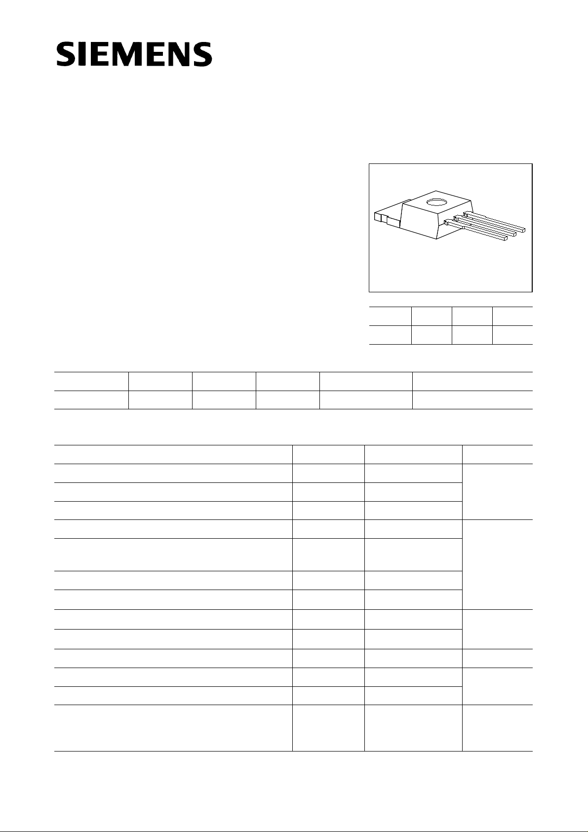
BTS 115A
Pin 1 2 3
GDS
3
2
1
Type
V
DS
I
D
R
DS(on)
Package Ordering Code
BTS 115A 50 V 15.5 A 0.12 Ω TO-220AB C67078-S5004-A2
Maximum Ratings
Parameter Symbol Values Unit
Drain-source voltage
Drain-gate voltage,
R
= 20 kΩ V
GS
Gate-source voltage
T
Continuous drain current,
= 25 °C I
C
ISO drain current
T
= 85 °C, VGS = 4.5 V, VDS = 0.5 V
C
T
Pulsed drain current,
Short circuit current,
Short circuit dissipation,
= 25 °C I
C
T
= – 55 ... + 150 °C
j
T
= – 55 ... + 150 °C
j
Power dissipation
Operating and storage temperature range
V
DS
DGR
V
GS
D
I
D-ISO
D puls
I
SC
P
SCmax
P
tot
T
j
, T
stg
50 V
50
± 10
15.5 A
3.2
62
37
550 W
50
– 55 ... + 150 °C
DIN humidity category, DIN 40 040 – E –
IEC climatic category, DIN IEC 68-1 – 55/150/56
Thermal resistance
Chip-case
Chip-ambient
R
R
th JC
th JA
≤ 2.5
≤ 75
K/W
Semiconductor Group 1 04.97
Page 2
BTS 115A
Electrical Characteristics
at Tj = 25 °C, unless otherwise specified.
Parameter Symbol Values Unit
min. typ. max.
Static Characteristics
Drain-source breakdown voltage
V
= 0, ID = 0.25 mA
GS
Gate threshold voltage
V
= V
, I
GS
DS
= 1.0 mA
D
Zero gate voltage drain current
V
= 0 V, VDS = 50 V
GS
T
= 25 °C
j
T
= 125 °C
j
Gate-source leakage current
V
= 20 V, VDS = 0
GS
T
= 25 °C
j
T
= 150 °C
j
Drain-source on-state resistance
V
= 4.5 V, ID = 7.8 A
GS
Dynamic Characteristics
Forward transconductance
V
≥ 2 × ID× R
DS
DS(on)max
, ID =7.8 A
Input capacitance
V
= 0, VDS = 25 V, f = 1 MHz
GS
Output capacitance
V
= 0, VDS = 25 V, f = 1 MHz
GS
Reverse transfer capacitance
V
= 0, VDS = 25 V, f = 1 MHz
GS
Turn-on time
V
= 30 V, VGS = 5 V, ID = 3 A, RGS = 50 Ω
CC
Turn-off time
V
= 30 V, VGS = 10 V, ID = 3 A, RGS = 50 Ω
CC
t
, (ton = t
on
t
, (t
off
off
= t
d(on)
d(off)
+ tr)
+ tf)
V
(BR)DSS
V
GS(th)
I
DSS
I
GSS
R
DS(on)
g
fs
C
iss
C
oss
C
rss
t
d(on)
t
r
t
d(off)
t
f
V
50 – –
1.5 2.0 2.5
µA
–
–
–
–
0.1
10
10
2
1.0
100
100
4
nA
µA
Ω
– 0.09 0.12
S
5.5 9.5 –
pF
– 550 735
– 220 320
– 85 150
–1525ns
– 70 100
–7090
–5070
Semiconductor Group 2
Page 3
BTS 115A
Electrical Characteristics (cont’d)
at Tj = 25 °C, unless otherwise specified.
Parameter Symbol Values Unit
min. typ. max.
Reverse Diode
Continuous source current
Pulsed source current
Diode forward on-voltage
I
= 34 A, VGS = 0
F
Reverse recovery time
I
= IS, diF/dt = 100 A/µs, VR = 30 V
F
Reverse recovery charge
I
= I S, diF/dt = 100 A/µs, VR = 30 V
F
Temperature Sensor
Forward voltage
I
= 5.0 mA, Tj = – 55 ... + 150 °C
TS(on)
Sensor override, tp≤ 100 µs
T
= – 55 ... + 160 °C
j
Forward current
T
= – 55 ... + 150 °C
j
Sensor override, tp≤ 100 µs
T
= – 55 ... + 160 °C
j
V
Holding current,
= 5 V, Tj = 25 °C
TS(off)
Switching temperature
V
= 5 V
TS
Turn-off time
V
= 5 V, I
TS
TS(on)
= 2 mA
T
= 150 °C
j
I
S
I
SM
V
SD
t
rr
Q
V
TS(on)
I
TS(on)
I
H
T
TS(on)
t
off
– – 15.5 A
––62
V
– 1.5 1.8
ns
–60–
rr
µC
– 0.10 –
V
1.3
–
–
1.4
10
mA
–
–
0.05
0.05
–
–
0.1
0.2
5
600
0.5
0.3
°C
150 – –
µs
0.5 – 2.5
Semiconductor Group 3
Page 4

BTS 115A
Examples for short-circuit protection
at Tj = – 55 ... + 150 °C, unless otherwise specified.
Parameter Symbol Examples Unit
12–
Drain-source voltage
Gate-source voltage
Short-circuit current
Short-circuit dissipation
Response time
T
= 25 °C, before short circuit
j
Short-circuit protection ISC = f (VDS)
Parameter:V
GS
DiagramtodetermineISCforTj=–55...+150°C
V
DS
V
GS
I
SC
P
SC
t
SC(off)
15 30 – V
5.0 3.5 –
37 17 – A
550 510 – W
25 25 –
Max. gate voltage V
Parameter: Tj= – 55 ... + 150 °C
GS(SC)
ms
= f (VDS)
Semiconductor Group 4
Page 5

BTS 115A
Max. power dissipation P
= f (TC)
tot
Typ. drain-source on-state resistance
R
= f (ID)
DS(on)
Parameter:V
GS
Typical output characteristics ID = f (VDS)
Parameter:tp =80µs
Safe operating area ID = f (VDS)
Parameter: D = 0.01, TC=25°C
Semiconductor Group 5
Page 6

BTS 115A
Drain-source on-state resistance
R
= f (Tj)
DS(on)
Parameter: ID= 7.8 A, VGS = 4.5 V
Gate threshold voltage V
GS(th)
= f (Tj)
Parameter:VDS = VGS, ID= – 1 mA
Typ. transfer characteristic
I
= f (VGS)
D
Parameter:tp = 80 µs, VDS = – 25 V
Typ. transconductance gfs = f (ID)
Parameter: tp = 80 µs, VDS = – 25 V
Semiconductor Group 6
Page 7

BTS 115A
Continuous drain current ID= f (TC)
Parameter: VGS≥ 4.5 V
Forward characteristics of reverse diode
I
= f (VSD)
F
Parameter:Tj,tp = 80 µs
Typ. gate-source leakage current
I
= f (TC)
GSS
Parameter: VGS = – 20 V, VDS = 0
Typ. capacitances C = f (VDS)
Parameter: VGS = 0, f = 1 MHz
Semiconductor Group 7
Page 8

BTS 115A
Transient thermal impedance Z
Parameter:D = tp/T
thJC
= f (tp)
Semiconductor Group 8
Page 9

BTS 115A
Package Outlines
TO 220 AB Ordering Code
Standard C67078-S5004-A2
9.9
9.5
3.7
2.8
17.5
12.8
1
2)
0.75
1) punch direction, burr max. 0.04
2) dip tinning
3) max. 14.5 by dip tinning press burr max. 0.05
4.6
1.05
2.542.54
4.4
1.3
1)
15.6
9.2
3)
13.5
0.5
2.4
GPT05155
TO 220 AB Ordering Code
SMD Version E 3045 C67078-S5004-A8
Semiconductor Group 9
 Loading...