

Page 1

Dual Differential Transceiver BTF1A
With Idle Bus Indicator
■
Features
Driver Features
■
Produces a logic zero in third state
■
400 mV difference voltage in third state
■
Two line drivers per package
■
Logic to convert TTL input logic levels to differential, pseudo-emmiter coupled logic (ECL) output
logic levels
■
No line loading when VCC = 0 V
■
High output driver for 50 Ω loads
■
200 mA short-circuit current (typical)
■
2.0 ns maximum propagation delay
■
<0.2 ns output skew (typical)
Receiver Features
■
Two line receivers per package
■
High input impedance ≅ 8 kΩ
■
Logic that converts differential input logic levels to
TTL output logic levels
■
4.0 ns maximum propagation delay
■
<0.20 V input sensitivity (typical)
−1.2 V to +7.2 V common-mode range
■
Common Device Features
■
Common enable for each driver/receiver pair
■
Operating temperature range: –40 °C to +125 °C
(wider than the 41 Series)
Electrostatic discharge (ESD) performance better
than the 41 Series
■
Lower power requirement than the 41 Series
Description
The BTF1A device is a dual differential transceiver
circuit that transmits and receives digital data over
balanced transmission lines and is compatible with
Lucent Technologies Microelectronics Group differential drivers and receivers. It is designed to provide
a strong logic zero when in the third state. The minimum difference voltage in the third state is 400 mV. It
is designed specifically for bus applications where a
well-defined logic state is needed when the bus is
idle. The driver puts out a logic
state mode, which is easily overriden by an active
buffer on the bus. When all the buffers on the bus are
inactive (third state), the signal on the bus is a
indicating that the bus is idle.
The dual drivers translate input TTL logic levels to differential pseudo-ECL output levels. The dual receiver
converts differential input logic levels to TTL output
levels. Each driver/receiver pair has its own common
enable control allowing serial data and a control clock
to be transmitted and received on a single integrated
circuit. The BTF1A tr ansceiv er re quires the customer
to supply termination resistors on the circuit board.
The powerdown loading characteristics of the
receiver input circuit are approximately 8 kΩ relative
to the power supplies; hence, it will not load the
transmission line when the circuit is powered down.
For those circuits with termination resistors, the line
will remain impedance matched when the circuit is
powered down. The driver does not load the line
when it is powered down.
Data Sheet
March 2001
when in the third
zero
zero
■
Single 5.0 V ± 5% supply
■
400 Mbits/s maximum data rate
■
Meets enhanced small device interface (ESDI)
standards
Page 2
Dual Differential Transceiver BTF1A
With Idle Bus Indicator
Pin Information
Data Sheet
March 2001
RO1
DI1
V
ED
ER
GND
DI2
RO2
1
2
CC
3
4
5
6
7
8
R1
D1
D2
R2
BTF1A
RI1
16
RI1
15
DO1
14
DO1
13
DO2
12
DO2
11
RI2
10
RI2
9
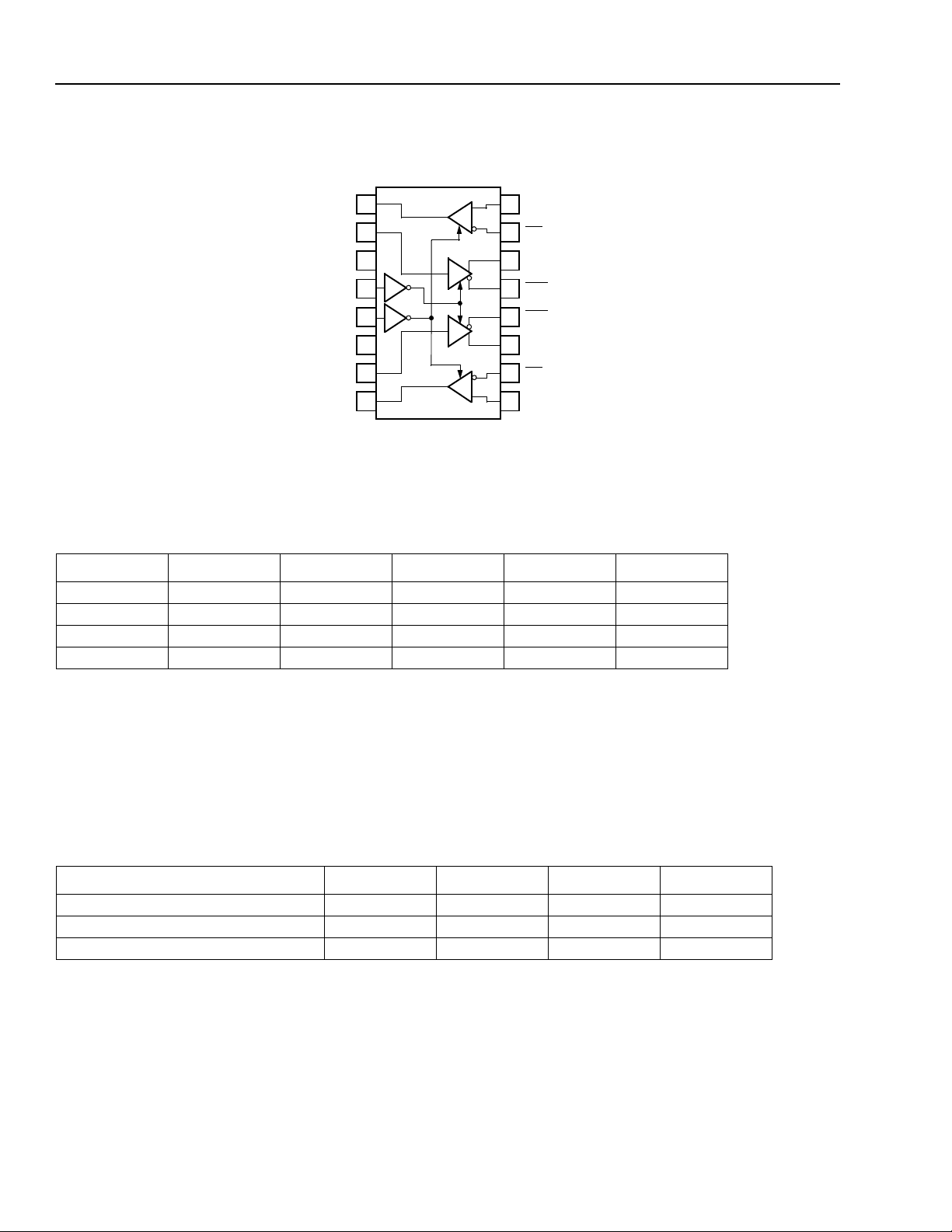
Figure 1. Differential Transceiver Logic Diagram
Table 1. Enable Truth Table
ED ER D1 D2 R1 R2
0 0 Active Active Active Active
1 0 Disabled Disabled Active Active
0 1 Active Active Disabled Disabled
1 1 Disabled Disabled Disabled Disabled
12-2747.a(F)
Absolute Maximum Ratings
Stresses in excess of the absolute maximum ratings can cause permanent damage to the device. These are absolute stress ratings only. Functional operation of the device is not implied at these or any other conditions in excess
of those given in the operational sections of the data sheet. Exposure to absolute maximum ratings for extended
periods can adversely affect device reliability.
Table 2. Absolute Maximum Ratings
Parameter Symbol Min Max Unit
Power Supply Voltage V
Ambient Operating Temperature T
Storage Temperature T
CC
A
stg
—6.5V
−40 125 °C
−55 150 °C
2 Agere Systems Inc.
Page 3

Data Sheet
March 2001
Dual Differential Transceiver BTF1A
With Idle Bus Indicator
Electrical Characteristics
For variations in electrical characteristics over the temperature range, see Figure 10 through Figure 12.
Table 3. Power Supply Current Characteristics
A
= −40 °C to +125 °C, V
T
CC
= 5 V ± 0.25 V.
Parameter Symbol Min Typ Max Unit
Power Supply Current (V
All Outputs Disabled
All Outputs Enabled
CC
= 5.5 V)
I
I
CC
CC
—
—
40
20
65
35
mA
mA
Third State
The BTF1A driver produces pseudo-ECL levels, and has a third-state mode, which is different than a conventional
TTL device. When a driver is placed in the third state, the base of the output transistors are pulled low, bringing the
outputs below the active-low level. The BTF1A is unique because it provides a logic zero at its output when in the
third state. If all the buffers on the bus are in the third state, the BTF1A is designed to deliver a logic zero to the bus
to act as an indicator that the bus is idle. The guaranteed zero level, Vdo
– Vdo, is 0.4 V.
Agere Systems Inc. 3
Page 4

Dual Differential Transceiver BTF1A
With Idle Bus Indicator
Data Sheet
March 2001
Electrical Characteristics
(continued)
Table 4. Driver Voltage and Current Characteristics
A
For variations in output voltage over the temperature range, see Figure 10 and Figure 11. T
= −40 °C to +125 °C.
Parameter Symbol Min Typ Max Unit
Output Voltages:
1
Low
1
High
:V
Differential Voltage (V
OH
– VOL)V
V
DIFF
OL
OH
OH –
V
1.4 V
CC
− 1.8 V
V
OH
− 1.1 V
CC
− 1V
OH
− 0.65 V
CC
− 0.8 V
0.65 1.1 1.4 V
Output Voltage Third State:
Difference Voltage Vdo
Third State, I
Output Voltages (T
1
Low
1
High
:V
OH
= –1.0 mA, VCC = 4.75 V V
A
Differential Voltage (V
- Vdo V
= 0 °C to 85 °C):
OH
– VOL)V
DIFZ
V
DIFF
OZ
OL
OH
0.4 0.6 — V
OL
——V
OH –
V
1.4 V
CC
− 1.5 V
V
OH
− 1.1 V
CC
− 1V
− 0.2 V
OH
− 0.8 V
CC
− 0.8 V
0.8 1.1 1.4 V
Input Voltages:
IH
OS
IH
IH
2
IL
3
IL
3
IL
2
IK
——0.8V
——0.8V
——0.7V
2.0 — — V
——−1.0 V
–100 — — mA
IL
——−400 µA
——20 µA
— — 100 µA
CC
Low, V
= 5.25 V: V
Data Input V
Enable Input V
High, V
Clamp, V
Short-circuit Output Current, V
Input Currents, V
Low, V
High, V
Reverse, V
1. Values are with terminations as per Figure 7.
2. The input levels and diff erence voltage provide zero noise immunity and should be tested only in a static, noise-free environment.
3. Test must be performed one lead at a time to prevent damage to the devi ce .
CC
= 4.75 V V
CC
= 4.75 V, II = –5.0 mA V
CC
= 5.25 V I
CC
= 5.25 V:
I
= 0.4 V I
I
= 2.7 V I
I
= 5.25 V I
4 Agere Systems Inc.
Page 5

Data Sheet
March 2001
Dual Differential Transceiver BTF1A
With Idle Bus Indicator
Electrical Characteristics
(continued)
Table 5. Receiver Voltage and Current Characteristics
OH
For variation in minimum V
and maximum VOL over the temperature range, see Figure 10. TA = –40 °C to +125 °C.
Parameter Symbol Min Typ Max Unit
CC
Output Voltages V
OL
Low, I
High, I
= 8.0 mA
OH
= −400 µA V
= 4.75 V:
1
OL
V
OH
——0.5V
2.4 — — V
Enable Input Voltages:
CC
Low, V
High, V
Clamp, V
Minimum Differential Input Voltages, V
−0.80 V < V
= 5.25 V V
CC
= 4.75 V V
CC
= 4.75 V, II = –5.0 mA V
IH – VIL
IH
< 7.2 V, −1.2 V < VIL < 6.8 V V
2
:
Input Offset Voltage V
Output Currents, V
Off-state (high Z), V
Off-state (high Z), V
CC
= 5.25 V:
O
= 0.4 V I
O
= 2.4 V I
Short Circuit I
Enable Input Currents, V
IN
Low, V
High, V
Reverse, V
= 0.4 V I
IN
= 2.7 V I
IN
= 5.5 V I
CC
= 5.25 V:
IL
IH
IK
TH
OFF
OZL
OZH
OS
IL
IH
IH
1
1
——0.7V
2.0 — — V
——−1.0 V
1
—0.10.20V
0.03 0.05 V
——–20µA
——20µA
3
–25 — –100 mA
— — –400 µA
——20µA
——100µA
Differential Input Currents:
IN
Low, V
High, V
1. The input levels and difference voltage provide zero noise immunity and should be tested only in a static, noise-free environment.
2. Outputs of unused receivers assume a logic 1 level when the inputs are left open. (It is recommended that all unused positive inputs
be tied to the positive power supply. No external series resistor is required.)
3. Test must be performed one lead at a time to prevent damage to the device.
= –1.2 V I
IN
= 7.2 V I
IL
IH
——−1.0 mA
——1.0mA
Agere Systems Inc. 5
Page 6

Dual Differential Transceiver BTF1A
With Idle Bus Indicator
Timing Characteristics
Data Sheet
March 2001
Table 6. Driver Timing Characteristics
P1
For t
and tP2 propagation delays over the temperature range, see Figure 13. Propagation delay test circuit con-
nected to output is shown in Figure 7. T
(See Figure 3 and Figure 4.)
A
= −40 °C to +125 °C, V
CC
= 5 V ± 0.25 V.
Parameter Symbol Min Typ Max Unit
Propagation Delay:
Input High to Output
Input Low to Output
1
1
2
P1
t
2
P2
t
0.8 1.2 2.0 ns
0.8 1.2 2.0 ns
Capacitive Delay ∆tp — 0.02 0.03 ns/pF
Disable Time (either E1 or E2):
High-to-High Impedance t
Low-to-High Impedance t
PHZ
PLZ
4812ns
4812ns
Enable Time (either E1 or E2):
High Impedance to High t
High Impedance to Low t
PZH
PZL
4812ns
4812ns
Output Skew:
P1
|t
– tP2|t
PHH – tPHL
|t
|, |t
PLH
PLL
– t
|t
Difference Between Drivers ∆t
Rise Time (20%—80%) t
Fall Time (80%—20%) t
1. CL = 5 pF. Capacitor is connected from each output to ground.
2. tP1 and tP2 are measured from the 1.5 V point of the input to the crossover point of the outputs (see Figure 3).
skew1
skew2
skew
tLH
tHL
—0.10.3ns
—0.20.5ns
——0.3ns
—0.7 2ns
—0.7 2ns
Table 7. Receiver Timing Characteristics
For propagation delays (t
PLH
and t
PHL
) over the temperature range, see Figure 14 and Figure 15. Propagation delay
test circuit connected to output is shown in Figure 8. T
(See Figure 5 and Figure 6.)
A
= −40 °C to +125 °C, V
CC
= 5 V ± 0.25 V.
Parameter Symbol M in Typ Ma x Unit
Propagation Delay:
Input to Output High t
Input to Output Low t
PLH
PHL
1.5 2.5 4.0 ns
1.5 2.5 4.0 ns
Pulse Width Distortion, ltpHL-tpLHI:
Load Capacitance (C
Load Capacitance (C
L
) = 15 pF tskew1 — — 0.7 ns
L
) = 150 pF tskew1 — — 4.0 ns
Output Waveform Skews:
Part-to-Part Skew, T
Part-to-Part Skew, T
A
= 75 °C ∆tskew1p-p — 0.8 1.4 ns
A
= –40 °C to +125 °C ∆tskew1p-p — — 1.5 ns
Same Part Skew ∆tskew — — 0.3 ns
Disable Time, C
High-to-high Impedance t
Low-to-high Impedance t
L
= 5 pF:
PHZ
PLZ
— 5 12 ns
— 5 12 ns
Enable Time:
High Impedance to High t
High Impedance to Low t
Rise Time (20%—80%) t
Fall Time (80%—20%) t
PZH
PZL
tLH
tHL
— 8 12 ns
— 8 12 ns
——3.0ns
——3.0ns
6 Agere Systems Inc.
Page 7

Data Sheet
March 2001
Dual Differential Transceiver BTF1A
With Idle Bus Indicator
Timing Characteristics
(continued)
7
(ns)
P
6
5
4
PLH
t
(TYP)
3
2
PHL
t
(TYP)
1
0
EXTRINSIC PROPAGATION DELAY, t
25 50 75 100 125 150
LOAD CAPACITANCE, C
L
(pF)
175 2000
12-3462(F)
Note: This graph is included as an aid to the system designers. Total circuit delay varies with load capacitance. The total delay is the sum of the
delay due to the external capacitance and the intrinsic delay of the device.
Figure 2. Typical Extrinsic Propagation Delay Versus Load Capacitance at 25 °C
INPUT
TRANSITION
OUTPUTS
OUTPUT
OUTPUT
OUTPUT
PHH
t
t
PHL
P1
t
80%
t
PLL
t
PLH
t
80%
20%
tLH
t
Figure 3. Driver Propagation Delay Timing
2.4 V
1.5 V
0.4 V
P2
OH
V
OL
V
OH
V
(VOH + VOL)/2
OL
V
OH
V
(VOH + VOL)/2
OL
V
OH
V
20%
tHL
t
OL
V
12-2677(F)
Agere Systems Inc. 7
Page 8

Dual Differential Transceiver BTF1A
With Idle Bus Indicator
Data Sheet
March 2001
Timing Characteristics
(continued)
ED
PHZ
OUTPUT
OUTPUT
– 0.4 V
t
OUTPUT
PLZ
t
Note: In the third state, OUTPUT is 0.4 V more negative than OUTPUT.
Figure 4. Driver Enable and Disable Timing
t
t
PZH
PZL
3.0 V
1.5 V
0.0 V
OH
V
OL
V
+ 0.2 V
OL
V
VOL – 0.1 V
OL
V
VOL – 0.1 V
12-2268.d(F)
INPUT
INPUT
OUTPUT
PHL
t
80%
20%
tHL
t
20%
Figure 5. Receiver Propagation Delay Timing
PLH
t
80%
3.7 V
3.2 V
2.7 V
OH
V
1.5 V
OL
V
tLH
t
12-2251.b(F)
8 Agere Systems Inc.
Page 9

Data Sheet
TO OUTPUT OF
DEVICE UNDER
TEST
C
L
15 pF*
5 k
Ω
2 k
Ω
+5 V
March 2001
Dual Differential Transceiver BTF1A
With Idle Bus Indicator
Timing Characteristics
E1*
†
E2
PHZ
t
OH
V
OUTPUT
OL
V
* E2 = 1 while E1 changes state.
†E1 = 0 while E2 changes state.
Test Conditions
(continued)
∆
V = 0.5 V
t
PZH
∆
V = 0.5 V
t
PLZ
∆
V = 0.5 V
Figure 6. Receiver Enable and Disable Timing
t
PZL
∆
V = 0.5 V
3 V
1.5 V
0 V
3 V
1.5 V
0 V
12-2538.b(F)
Parametric values specified under the Electrical Characteristics and Timing Characteristics sections for the
data transmission driver devices are measured with the
following output load circuits.
Ω
100
DO DO
200
Ω
200
Ω
12-2271.a(F)
Figure 7. Driver Propagation Delay Test Circuit
12-2249(F)
* Includes probe and jig capacitances.
Note: All 458E, IN4148, or equivalent diodes.
Figure 8. Receiver Propagation Delay Test Circuit
Agere Systems Inc. 9
Page 10

Dual Differential Transceiver BTF1A
With Idle Bus Indicator
Data Sheet
March 2001
Output Characteristics
Figure 9 illustrates typical driver output characteristics.
Included are load lines for two typical termination configurations.
OUTPUT VOLTAGE (V)
VCC – 2 V VCC – 1 V V
OH
V
Y LOAD
OL
V
π
LOAD
A. Output Current vs. Output Voltage for Loads
Shown in B and C
DO
60
Ω
90
60
Ω
DO
Ω
B. Y Load
CC
OUTPUT CURRENT (mA)
10
20
30
40
12-2269(F)
12-2270(F)
Temperature Characteristics
0
CC
–0.5
–1.0
–1.5
–2.0
OUTPUT VOLTAGE RELATIVE TO V
–2.5
Figure 10. V
1.2
1.0
0.8
0.6
VOH MAX
VOH MIN
VOL MAX
–25 0 25 50 75 100
TEMPERATURE (°C)
OL
and V
OH
Extremes for Drivers vs.
Temperature for 100 Ω Load
VOH – VOL TYP
VOH – VOL MIN
VOL MIN
125 150–50
2-3467(F)
Ω
100
DO DO
200
Ω
π
C.
Load
200
Ω
12-2271.a(F)
0.4
DIFFERENTIAL VOLTAGE (V)
0
–25 0 25 50 75 100
TEMPERATURE (°C)
Figure 11. Differential Voltage (VOH – VOL) for
125 150–50
12-3468(F)
Drivers vs. Temperature
Figure 9. Driver Output Current vs. Voltage
Characteristics
1010 Agere Systems Inc.
Page 11

Data Sheet
3.8
–25 0 25 50 75 100
1.00
3.00
TEMPERATURE (°C)
2.00
1.50
2.50
4.00
125 150
3.50
MAX
TYP
MIN
PROPAGATION DELAY (ns)
–50
–25 0 25 50 75
1.00
1.50
2.00
4.00
125 150–50
2.50
3.00
3.50
MAX
TYP
MIN
PROPAGATION DELAY (ns)
TEMPERATURE (°C)
100
March 2001
Dual Differential Transceiver BTF1A
With Idle Bus Indicator
Temperature Characteristics
3.6
3.2
2.8
2.4
2.0
1.6
VOLTAGE (V)
1.2
0.8
0.4
0.0
–25 0 25 50 75 100
–50
Figure 12. Minimum V
Temperature at V
Receiver
IOH MIN
IOL MAX
TEMPERATURE (°C)
OH
and Maximum V
CC
= 4.5 V for the
(continued)
125 150
12-3464.a(F)
OL
vs.
12-3465(F)
Figure 14. Propagation Delay for a High Output
PLH
(t
) vs. Temperature at VCC = 5.0 V for
the Receivers
2.3
2.1
PROPAGATION DELAY (ns)
1.9
1.7
1.5
1.3
1.1
0.9
0.7
0.5
0.3
RANGE FOR tP1 AND t
MAX
MIN
–25 0 25 50 75 100
TEMPERATURE (°C)
P2
125 150–50
12-3469.a(F)
Figure 13. Min and Max for tP1 and tP2 Propagation
Delays vs. Temperature for the Driver
12-3466(F)
Figure 15. Propagation Delay for a Low Output
PHL
(t
) vs. Temperature at VCC = 5.0 V for
the Receivers
Agere Systems Inc. 11
Page 12

Dual Differential Transceiver BTF1A
With Idle Bus Indicator
Data Sheet
March 2001
Handling Precautions
CAUTION: This device is susceptible to damage as a result of ESD. Take proper precautions during both
handling and testing. Follow guidelines such as JEDEC Publication No. 108-A (Dec. 1988).
When handling and mounting line driver products, proper precautions should be taken to avoid exposure to ESD.
The user should adhere to the following basic rules for ESD control:
1. Assume that all electronic components are sensitive to ESD damage.
2. Never touch a sensitive component unless properly grounded.
3. Never transport, store, or handle sensitive components except in a static-safe environment.
ESD Failure Models
Lucent employs two models for ESD events that can cause device damage or failure:
1. A human body model (HBM) that is used by most of the industry for ESD-susceptibility testing and protectiondesign evaluation. ESD voltage thresholds are dependent on the critical parameters used to define the model.
A standard HBM (resistance = 1500 Ω, capacitance = 100 pF) is widely used and, therefore, can be used for
comparison purposes.
2. A charged-device model (CDM), which many believe is the better simulator of electronics manufacturing exposure.
Table 8 and Table 9 illustrate the role these two models play in the overall prevention of ESD damage. HBM ESD
testing is intended to simulate an ESD event from a charged person. The CDM ESD testing simulates charging and
discharging events that occur in production equipment and processes, e.g., an integrated circuit sliding down a
shipping tube.
The HBM ESD threshold voltage presented here was obtained by using these circuit parameters.
Table 8. Typical ESD Thresholds for Data Transmission Transceivers
Device HBM Threshold CDM Threshold
Differential Inputs >800 >1000
All Other Pins >2000 >1000
Table 9. ESD Damage Protection
ESD Threat Controls
Personnel Processes
Control
Model
Wrist straps
ESD shoes
Antistatic flooring
Human body model (HBM) Charged-device model (CDM)
Static-dissipative materials
Air ionization
12 Agere Systems Inc.
Page 13

Data Sheet
March 2001
Dual Differential Transceiver BTF1A
With Idle Bus Indicator
Latch Up
Latch up evaluation has been performed on the data transmission receivers. Latch up testing determines if the
power-supply current exceeds the specified maximum due to the application of a stress to the device under test. A
device is considered susceptible to latch up if the power supply current exceeds the maximum level and remains at
that level after the stress is removed.
Lucent performs latch up testing per an internal test method which is consistent with JEDEC Standard No. 17 (previously JC-40.2)
Latch up evaluation involves three separate stresses to evaluate latch up susceptibility levels:
1. dc current stressing of input and output pins.
2. Power supply slew rate.
3. Power supply overvoltage.
Table 10. Latch Up Test Criteria and Test Results
CMOS Latch Up Standardized Test Procedure
.
Data Transmission
Receiver ICs
Minimum Criteria
Test Results
dc Current Stress
of I/O Pins
≥150 mA ≤1 µs ≥1.75 x Vmax
≥250 mA ≤100 ns ≥2.25 x Vmax
Power Supply
Slew Rate
Power Supply
Overvoltage
Agere Systems Inc. 13
Page 14

Dual Differential Transceiver BTF1A
With Idle Bus Indicator
Outline Diagrams
16-Pin SOIC (SONB/SOG)
Dimensions are in millimeters.
L
N
1
PIN #1 IDENTIFIER ZONE
Data Sheet
March 2001
B
W
H
SEATING PLANE
1.27 TYP
Package
Description
Small-Outline,
0.10
Number of
Pins
(N)
0.51 MAX
Maximum Length
(L)
0.28 MAX
Package Dimensions
Maximum Width
Without Leads
Maximum Width
Including Leads
(B)
16 10.49 7.62 10.64 2.67
(W)
0.61
5-4414(F)
Maximum Height
Above Board
(H)
Gull-Wing
(SOG)
Note: The dimensions in this oultine diagram are intended for informational purposes only . For detailed schematics to assist your design efforts,
please contact your Lucent Technologies sales representative.
14 Agere Systems Inc.
Page 15

Data Sheet
DIP
SOIC/NB
J-LEAD SOIC/GULL WING
AIRFLOW (ft/min)
200 400 600 800 1000 12000
40
50
60
70
80
90
100
110
120
130
140
THERMAL RESISTANCE
Θ
ja
(
°
C/W)
March 2001
Dual Differential Transceiver BTF1A
With Idle Bus Indicator
Power Dissipation
System designers incorporating Lucent data transmission drivers in their applications should be aware of
package and thermal information associated with these
components.
Proper thermal management is essential to the longterm reliability of any plastic encapsulated integrated
circuit. Thermal management is especially important
for surface-mount devices, given the increasing circuit
pack density and resulting higher thermal density. A
key aspect of thermal management involves the junction temperature (silicon temperature) of the integrated
circuit.
Several factors contribute to the resulting junction temperature of an integrated circuit:
■
Ambient use temperature
■
Device power dissipation
■
Component placement on the board
■
Thermal properties of the board
■
Thermal impedance of the package
Thermal impedance of the package is referred to as
ja
Θ
and is measured in °C rise in junction temperature
per watt of power dissipation. Thermal impedance is
also a function of airflow present in system application.
The following equation can be used to estimate the
junction temperature of any device:
The power dissipated in the output is a function of the:
■
Termination scheme on the outputs
■
Termination resistors
■
Duty cycle of the output
Package thermal impedance depends on:
■
Airflow
■
Package type (e.g., DIP, SOIC, SOIC/NB)
The junction temperature can be calculated using the
previous equation, after power dissipation levels and
package thermal impedances are known.
Figure 16 illustrates the thermal impedance estimates
for the various package types as a function of airflow.
This figure shows that package thermal impedance is
higher for the narrow-body SOIC package. Particular
attention should, therefore, be paid to the thermal management issues when using this package type.
In general, system designers should attempt to maintain junction temperature below 125 °C. The following
factors should be used to determine if specific data
transmission drivers in particular package types meet
the system reliability objectives:
■
System ambient temperature
■
Power dissipation
■
Pac kage type
■
Airflow
j
T
= TA + PD
Θ
ja
where:
j
T
is device junction temperature (°C).
A
T
is ambient temperature (°C).
D
P
is power dissipation (W).
ja
Θ
is package thermal impedance (junction to
ambient
—
°C/W).
The power dissipation estimate is derived from two factors:
■
Internal device power
■
Power associated with output terminations
Multiplying I
CC
times VCC provides an estimate of
12-2753(F)
internal power dissipation.
Agere Systems Inc. 15
Figure 16. Power Dissipation
Page 16

Dual Differential Transceiver BTF1A
With Idle Bus Indicator
Ordering Information
Data Sheet
March 2001
Part Number Driver
Terminating
1
Receiver
Terminating
2
Package Type Comcode
BTF1A16G None None 16-pin, Plastic SOIC 108648861
BTF1A16G-TR None None Tape and Reel SOIC 108698887
1. Indicates on-chip output terminating resistors from each driver output to ground.
2. Indicates on-chip input terminations across receiver inputs.
For additional information, contact your Agere Systems Account Ma na ger or the following:
INTERNET:
E-MAIL:
N. AMERICA: Agere Systems Inc., 555 Union Boulevard, Room 30L-15P-BA, Allentown, PA 18109-3286
ASIA PACIFIC: Agere Systems Singapore Pte. Ltd., 77 Science Park Drive, #03-18 Cintech III, Singapore 118256
CHINA: Agere Systems (Shanghai) Co., Ltd., 33/F Jin Mao Tower, 88 Century Boulevard Pudong, Shanghai 200121 PRC
JAPAN: Agere Systems Japan Ltd., 7-18, Higashi-Gotanda 2-chome, Shinagawa-ku, Tokyo 141, Japan
EUROPE: Data Requests: DATALINE:
Agere Systems Inc. reserves the right to make changes to the product(s) or information contained herein without notice. No liability is assumed as a result of their use or application.
Copyright © 2001 Agere Systems Inc.
All Rights Reserved
Printed in U.S.A.
http://www.agere.com
docmaster@micro.lucent.com
1-800-372-2447
Tel. (65) 778 8833
Tel. (86) 21 50471212
Tel. (81) 3 5421 1600
Tech ni cal Inquiries:GERMANY:
, FAX 610-712-4106 (In CANADA:
, FAX (65) 777 7495
, FAX (86) 21 50472266
, FAX (81) 3 5421 1700
Tel. (44) 7000 582 368
FRANCE:
(39) 02 6608131
ITALY:
(49) 89 95086 0
(33) 1 40 83 68 00
(Milan), SPAIN:
1-800-553-2448
, FAX (44) 1189 328 148
(Munich), UNITED KINGDOM:
(Paris), SWEDEN:
, FAX 610-712-4106)
(46) 8 594 607 00
(34) 1 807 1441
(Madrid)
(44) 1344 865 900
(Stockholm), FINLAND:
(Ascot),
(358) 9 3507670
(Helsinki),
March 2001
DS01-068ANET-1 (Replaces DS01-068ANET)
 Loading...