

Datasheet BTB41-800B, BTB41-600B, BTA41-800B, BTA41-600B Datasheet (SGS Thomson Microelectronics)
Page 1
BTA40 and BTA/BTB41 Series
STANDARD 40A TRIACS
MAIN FEATURES:
Symbol Value Unit
I
T(RMS)
V
DRM/VRRM
I
GT (Q1)
40 A
600 and 800 V
50 mA
DESCRIPTION
Available in high power packages, the BTA/
BTB40-41 series is suitable for general purpose
AC power switching. They can be used as an ON/
OFF function in applications such as static relays,
heating regulation, water heaters, induction motor
starting circuits, welding equipment... or for phase
control operation in high power motor speed controllers, soft start circuits...
Thanks to their clip assembly technique, they
provide a superior performance in surge current
handling capabilities.
By using an internal ceramic pad, the BTA series
provides voltage insulated tab (rated at 2500 V
RMS) complying with UL standards (File ref.:
E81734).
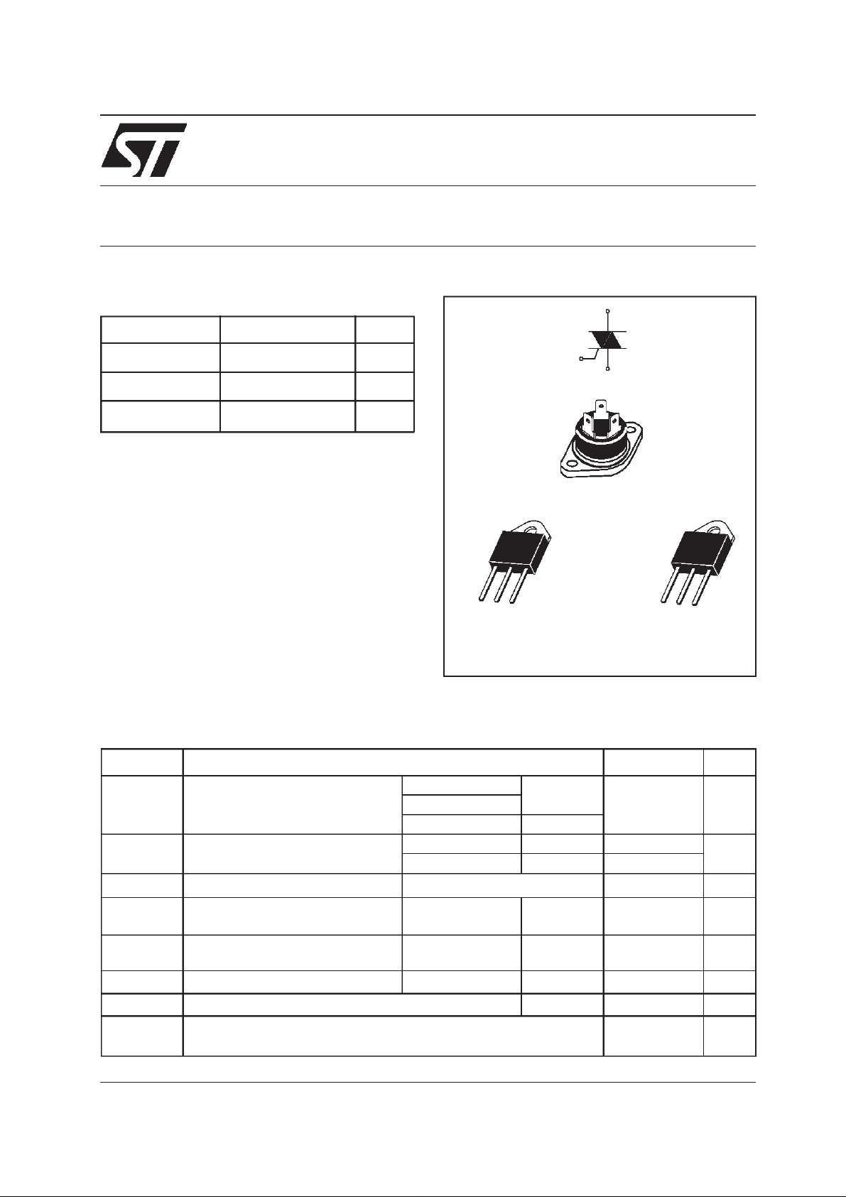
A1
A2
G
TOP3 Insulated
(BTA41)
A2
G
A1
A1
G
RD91
(BTA40)
A2
A1
A2
(BTB41)
A2
G
TOP3
ABSOLUTE MAXIMUM RATINGS
Symbol Parameter Value Unit
I
T(RMS)
I
TSM
I tI
dI/dt
V
DSM/VRSM
I
GM
P
G(AV)
T
stg
T
RMS on-state current
(full sine wave)
Non repetitive surge peak on-state
current (full cycle, Tj initial = 25°C)
t Valuefor fusing
Critical rate of rise of on-state current
I
=2xIGT,tr≤100 ns
G
Non repetitive surge peak off-state
voltage
Peak gate current tp = 20 µs Tj = 125°C8 A
Averagegate power dissipation Tj = 125°C1 W
Storage junction temperature range
Operating junction temperature range
j
October 2001 - Ed: 4
RD91
TOP3
Tc = 80°C
40
TOP3 Ins. Tc = 70°C
F = 60 Hz t = 16.7 ms 420 A
F = 50 Hz t = 20 ms 400
tp = 10 ms 880
F = 120 Hz Tj = 125°C50A/µs
V
tp = 10 ms Tj = 25°C
DRM/VRRM
+ 100
- 40 to + 150
- 40 to + 125
A
A
V
°C
s
1/6
Page 2
BTA40 and BTA/BTB41 Series
ELECTRICAL CHARACTERISTICS (Tj = 25°C, unless otherwise specified)
Symbol Test Conditions Quadrant Value Unit
(1)
I
GT
V
GT
V
GD
IH(2)
I
dV/dt (2) V
V
=12V RL=33Ω
D
VD=V
DRMRL
= 500 mA
I
T
IG= 1.2 I
L
=67%V
D
= 3.3 kΩ Tj = 125°C
GT
gate open Tj = 125°C
DRM
(dV/dt)c (2) (dI/dt)c = 20 A/ms Tj = 125°C MIN. 10 V/µs
STATIC CHARACTERISTICS
Symbol Test Conditions Value Unit
(2) ITM=60A tp=380µs
V
TM
V
(2)
to
Rd(2)
I
DRM
I
RRM
Threshold voltage Tj = 125°C MAX. 0.85 V
Dynamic resistance Tj = 125°C MAX. 10 mΩ
V
DRM=VRRM
I - II - III
IV
MAX.
50
100
mA
ALL MAX. 1.3 V
ALL MIN.
0.2 V
MAX. 80 mA
I - III - IV MAX. 70 mA
II 160
MIN. 500 V/µs
Tj = 25°C MAX. 1.55 V
Tj = 25°C
Tj = 125°C5mA
MAX.
5 µA
Note 1: minimum IGT is guaranted at 5% of IGT max.
Note 2: for both polarities of A2 referenced to A1
THERMAL RESISTANCES
Symbol Parameter Value Unit
R
th(j-c)
Junction to case (AC) RD91 (Insulated)
TOP3
0.9
TOP3 Insulated 1.2
R
th(j-a)
Junction to ambient TOP3
TOP3 Insulated
50
PRODUCT SELECTOR
Voltage (xxx)
Part Number
600 V 800 V
BTA40-xxxB X X 50 mA Standard RD91
BTA/BTB41-xxxB X X 50 mA Standard TOP3
BTB: Non insulated TOP3 package
Sensitivity Type
Package
°C/W
°C/W
2/6
Page 3

ORDERING INFORMATION
TRIAC
SERIES
INSULATION:
A: insulated
B: non insulated
OTHER INFORMATION
BTA40 and BTA/BTB41 Series
BT A 40 - 600 B
SENSITIVITY:
B: 50mA
VOLTAGE:
600: 600V
800: 800V
CURRENT:
40: 40A in RD91
41: 40A in TOP3
Part Number Marking Weight
BTA40-xxxB BTA40xxxB 20.0 g 25 Bulk
BTA/BTB41-xxxB BTA/BTB41xxxB 4.5 g 120 Bulk
Note: xxx= voltage
Fig. 1: Maximum power dissipation versus RMS
on-state current (full cycle).
P (W)
50
40
30
20
10
IT(RMS) (A)
0
0 5 10 15 20 25 30 35 40
Fig. 2: RMS on-state current versus case
temperature (full cycle).
IT(RMS) (A)
45
40
35
30
25
20
15
10
5
0
0 25 50 75 100 125
Base
quantity
BTA41
Tc(°C)
Packing
mode
BTA40/BTB41
3/6
Page 4

BTA40 and BTA/BTB41 Series
Fig. 3: Relative variation of thermal impedance
versus pulse duration.
K=[Zth/Rth]
1E+0
Zth(j-c)
1E-1
Zth(j-a)
BTA/BTB41
1E-2
tp (s)
1E-3
1E-3 1E-2 1E-1 1E+0 1E+1 1E+2 5E+2
Fig. 5: Surge peak on-state current versus
number of cycles.
ITSM (A)
450
400
350
300
Non repetitive
Tj initial=25°C
250
200
150
100
50
0
1 10 100 1000
Repetitive
Tc=70°C
Number of cycles
t=20ms
One cycle
Fig. 4: On-state characteristics (maximum
values).
ITM (A)
400
100
10
Tj max
Tj=25°C
Tj max.:
Vto = 0.85 V
VTM (V)
1
0.5 1.0 1.5 2.0 2.5 3.0 3.5 4.0 4.5 5.0
Rd = 10 mΩ
Fig. 6: Non-repetitive surge peak on-state
current for a sinusoidal pulse with width
tp < 10 ms, and corresponding value of I t.
ITSM (A),
3000
1000
100
0.01 0.10 1.00 10.00
I t
dI/dt limitation:
50A/µs
(A s)
tp (ms)
ITSM
I t
Tj initial=25°C
Fig. 7 : Relative variation of gate t rigger current,
holding current and l atching current versus
junction temperature (typical values).
IGT,IH,IL[Tj]/ IGT,IH,IL [Tj=25°C]
2.5
2.0
1.5
1.0
0.5
0.0
-40 -20 0 20 40 60 80 100 120 140
4/6
IGT
IH & IL
Tj(°C)
Fig. 8:Relativevariationofcritical rateofdecrease
of maincurrentversus(dV/dt)c(typical values).
(dI/dt)c [(dV/dt)c] / Specified (dI/dt)c
2.0
1.8
1.6
1.4
1.2
1.0
0.8
0.6
0.4
0.1 1.0 10.0 100.0
(dV/dt)c (V/µs)
Page 5

Fig. 9: Relative variation of critical rate of
decrease of main current versus junction
temperature.
(dI/dt)c [Tj] / (dI/dt)c [Tj specified]
6
5
4
3
2
BTA40 and BTA/BTB41 Series
1
0
0 25 50 75 100 125
Tj (°C)
PACKAGE MECHANICAL DATA
RD91 (Plastic)
L2 L1
B2
C
C2
N2
E3
A2
B1
C1
A1
N1
B
F
I
A
DIMENSIONS
REF.
Millimeters Inches
Min. Max. Min. Max.
A 40.00 1.575
A1 29.90 30.30 1.177 1.193
A2 22.00 0.867
B 27.00 1.063
B1 13.50 16.50 0.531 0.650
B2 24.00 0.945
C 14.00 0.551
C1 3.50 0.138
C2 1.95 3.00 0.077 0.118
E3 0.70 0.90 0.027 0.035
F 4.00 4.50 0.157 0.177
I 11.20 13.60 0.441 0.535
L1 3.10 3.50 0.122 0.138
L2 1.70 1.90 0.067 0.075
N1 33° 43° 33° 43°
N2 28° 38° 28° 38°
5/6
Page 6

BTA40 and BTA/BTB41 Series
PACKAGE MECHANICAL DATA
TOP3 Ins.(Plastic)
DIMENSIONS
REF.
Millimeters Inches
Min. Typ. Max. Min. Typ. Max.
A 4.4 4.6 0.173 0.181
B 1.45 1.55 0.057 0.061
C 14.35 15.60 0.565 0.614
D 0.5 0.7 0.020 0.028
E 2.7 2.9 0.106 0.114
F 15.8 16.5 0.622 0.650
G 20.4 21.1 0.815 0.831
H 15.1 15.5 0.594 0.610
J 5.4 5.65 0.213 0.222
K 3.4 3.65 0.134 0.144
L 4.08 4.17 0.161 0.164
P 1.20 1.40 0.047 0.055
R 4.60 0.181
Information furnished is believed to be accurate and reliable. However, STMicroelectronics assumes no responsibility for the consequences
of use ofsuch information nor forany infringement ofpatents or other rights of third parties whichmay result from its use. No license isgranted
by implication or otherwise under any patent or patent rights of STMicroelectronics. Specifications mentioned in this publication are subject
to change without notice. This publication supersedes and replaces all information previously supplied. STMicroelectronics products are not
authorized for use as critical components in life support devices or systems without express written approval of STMicroelectronics.
The ST logo is a registered trademark of STMicroelectronics
2001 STMicroelectronics - Printed in Italy - All Rights Reserved
Australia - Brazil - China - Finland - France- Germany - Hong Kong - India - Italy - Japan - Malaysia
Malta - Morocco - Singapore - Spain - Sweden - Switzerland - United Kingdom - U.S.A
STMicroelectronics GROUP OF COMPANIES
http://www.st.com
6/6
 Loading...