

Page 1
Bt8954
Voice Pair Gain Framer
The Bt8954 framer has been tailored specifically to meet the needs of voice pair gain
systems (also referred to as “cable relief systems” and “digital subscriber line carriers”)
by providing a direct connection to the DSL modem and the CODEC. It performs data,
clock, and format conversions necessary to construct a Pulse Code Multiplexed (PCM)
channel from a Symmetrical Digital Subscriber Line (SDSL) or a High-Bit-Rate Digital
Subscriber Line (HDSL) channel. The PCM channel consists of transmit and receive
data, clock, and frame sync signals configured for 2–18 voice channels. The PCM
channel connects directly to popular PCM codecs. The Digital Subscriber Line (DSL)
channel interface consists of serial data and clock connected to a RS8973, Bt8970 or a
Bt8960 DSL Transceiver. The Bt8954 supports clear and compressed voice system.
When coupled with a Bt8960, the Bt8954 provides PCM4 functions at greater than 5 km
reach with no voice compression, allowing V.34 modem operation.
At one end, Bt8954 multiplexes payload data from several PCM codecs with the
appropriate overhead and signaling bits into one transport frame that is passed on to the
bit-pump, for transport over a single twisted pair. At the other end, Bt8954
demultiplexes the DSL bit stream into payload data sent to the PCM codec, and
overhead data written into microcomputer-accessible registers.
Embedded Operations Channel (EOC) and signaling overhead can be inserted via the
Microcomputer Interface (MCI). Control and status registers are accessed via the MCI.
One common register group configures the PCM interface formatter, Phase-Locked
Loop (PLL), and PCM Loopback (LB). Another group of DSL channel registers
configures the elastic store FIFOs, overhead muxes, receive framer, payload mapper , and
the DSL loopback. Status registers monitor received overhead, PLL, FIFO, and framer
operations, including CRC and FEBE error counts.
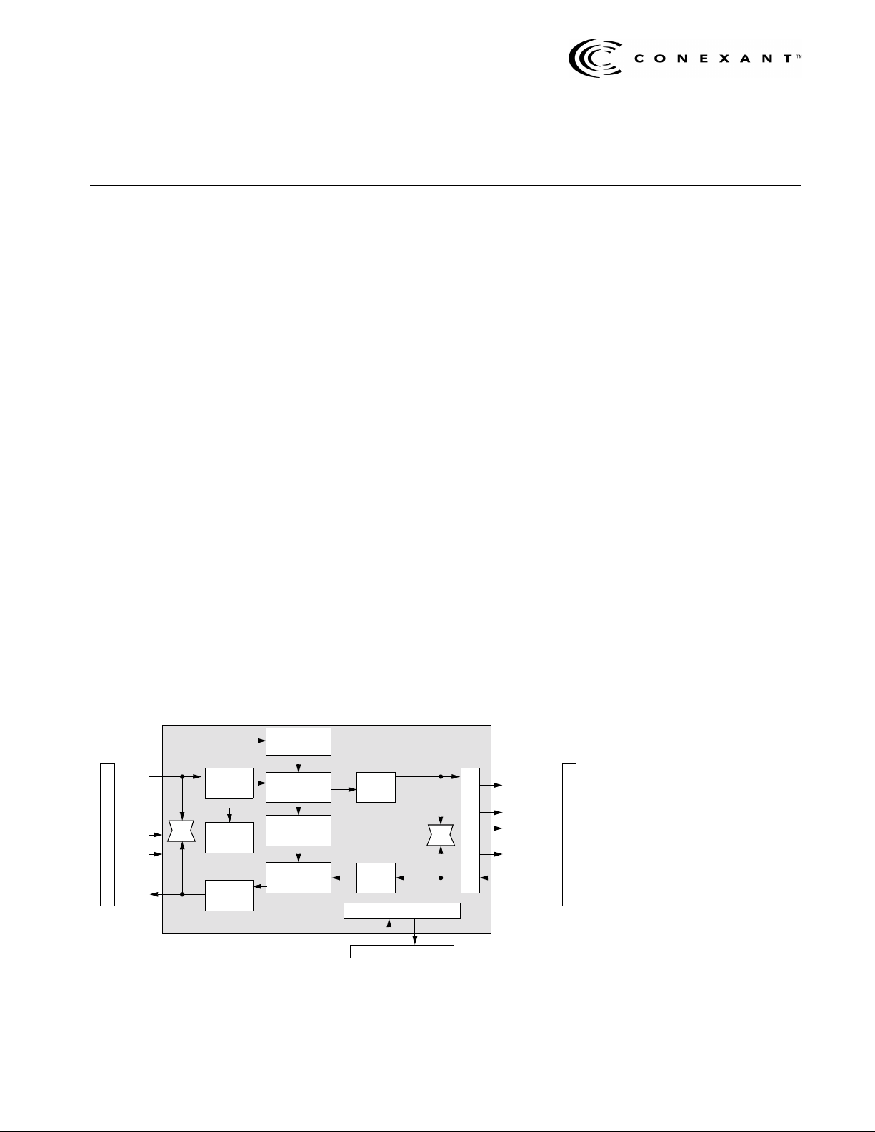
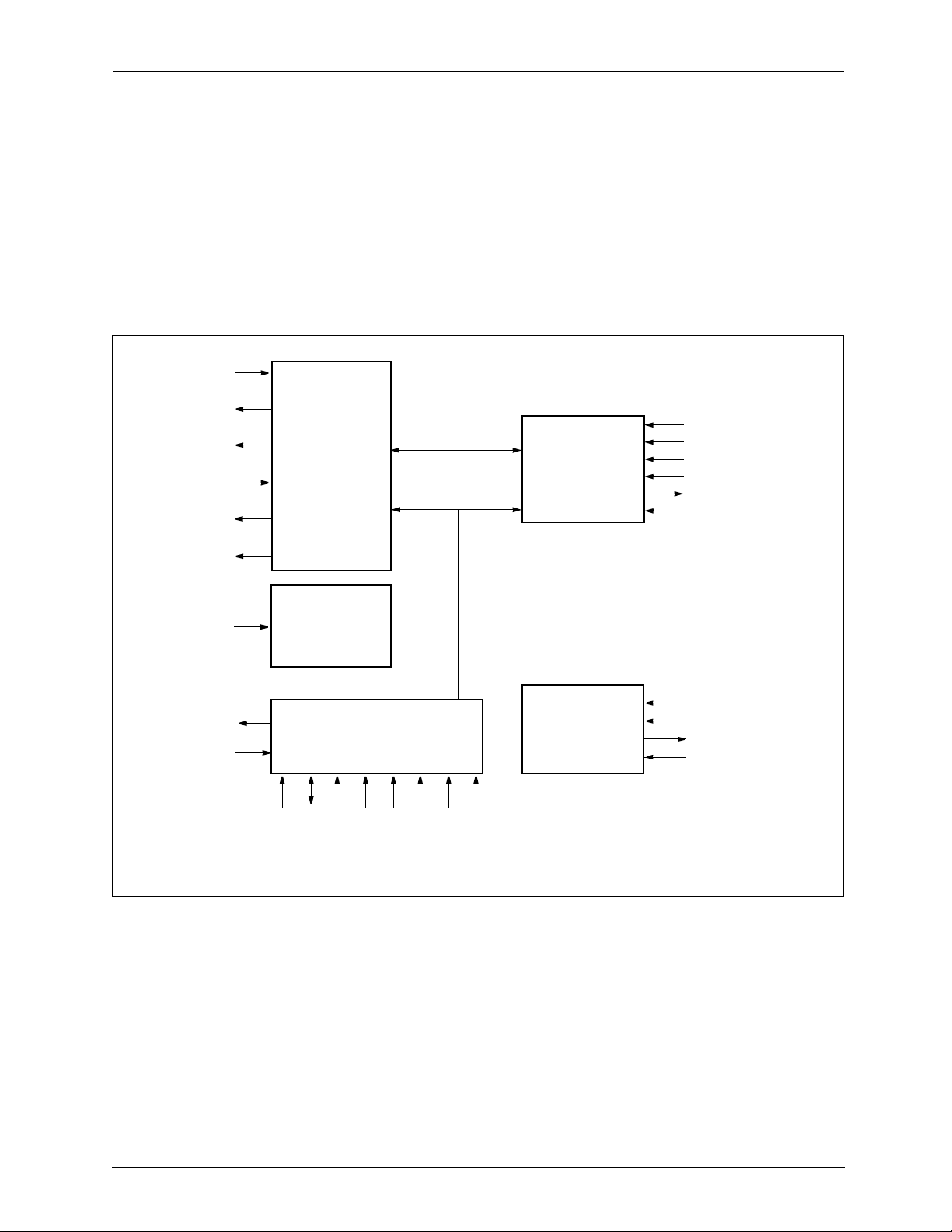
Functional Block Diagram
Receive
Framer
DSL Bit Pump
RDAT
HCLK
BCLK
QCLK
TDAT
LB
2B1Q
Decoder
PLL
2B1Q
Encoder
Payload
Demux
OH/Signaling
Registers
Payload
Mux
PCM
RFIFO
LB
PCM
TFIFO
Microcomputer Interface
PCM Formatter
PCMR
ADPCMCK
PCMCLK
PCMF[18:1]
PCMT
ADPCM/PCM Codecs
Distinguishing Features
• Voice Pair Gain Framer
– Frames and transports PCM data
streams over 12–18,000 ft.
(3.7–5.5 km) distances when
coupled with Bt8960 or Bt8970
• PCM Interface
– Supports popular PCM codecs
– Programmable payload to
support 2–18 64 kbps voice
channels
– 2.048, 1.536 MHz PCM reference
clock generation
– 6.144, 8.192, 20.48 MHz ADPCM
reference clock generation
• DSL Interface
– Connects to Bt8960 or Bt8970
– Supports 160–1168 kbps bit rates
– Error performance monitoring
– Auto tip/ring reversal
• Microcomputer Interface
– Glueless interface to Intel 8051
and Motorola 68302 processors
– Access to overhead and signaling
registers
• Supports ADPCM codecs (32 kbps)
• PCM and DSL loopbacks
• CMOS technology, 5 V operation
• Low-power operation
– Enables compatibility with
line-powered systems
• 68-pin PLCC
• JTAG/IEEE Std 1149.1-1990
• –40 °C to +85 °C operation
Applications
• Voice Pair Gain Systems (Clear)
– PCM2, PCM4(PCM1+3), PCM6,
– PCM8, PCM10/11, PCM12,
PCM18
• ADPCM Voice Pair Gain Systems
(Compressed)
– ADPCM12, ADPCM24, ADPCM36
Microcomputer
Data Sheet N8954DSC
April 7, 1999
Page 2

Ordering Information
Model Number Package Ambient Temperature
Bt8954 68-Pin Plastic Leaded Chip Carrier (PLCC) –40 °C to +85 °C
Information provided by Conexant Systems, Inc. (Conexant) is believed to be accurate and reliable. However, no responsibility is
assumed by Conexant for its use, nor any infringement of patents or other rights of third parties which may result from its use. No
license is granted by implication or otherwise under any patent rights of Conexant other than for circuitry embodied in Conexant
products. Conexant reserves the right to change circuitry at any time without notice. This document is subject to change without
notice.
Conexant and “What’s Next in Communications Technologies” are trademarks of Conexant Systems, Inc.
Product names or services listed in this publication are for identification purposes only, and may be trademarks or registered
trademarks of their respective companies. All other marks mentioned herein are the property of their respective holders.
© 1999 Conexant Systems, Inc.
Printed in U.S.A.
All Rights Reserved
Reader Response:
To improve the quality of our publications, we welcome your f eedbac k. Please send comments or
suggestions via e-mail to Conexant Reader Response@conexant.com. Sorry, we can't answer your technical
questions at this address. Please contact your local Conexant sales office or local field applications engineer if you
have technical questions.
N8954DSC
Conexant
Page 3

Table of Contents
Table of Contents
List of Figures
List of Tables
1.0 DSL Systems
1.1 Voice Pair Gain Applications
1.1.1 Repeaters
1.1.2 Subscriber Modem
1.2 System Interfaces
2.0 Pin Descriptions
. . . . . . . . . . . . . . . . . . . . . . . . . . . . . . . . . . . . . . . . . . . . . . . . . . . . . . . . . . . . . . . . iii
. . . . . . . . . . . . . . . . . . . . . . . . . . . . . . . . . . . . . . . . . . . . . . . . . . . . . . . . . . . . . . . . . . vii
. . . . . . . . . . . . . . . . . . . . . . . . . . . . . . . . . . . . . . . . . . . . . . . . . . . . . . . . . . . . . . . . . . . . ix
. . . . . . . . . . . . . . . . . . . . . . . . . . . . . . . . . . . . . . . . . . . . . . . . . . . . . . . . . . . . . . . . . . . 1-1
. . . . . . . . . . . . . . . . . . . . . . . . . . . . . . . . . . . . . . . . . . . . . . . . . . . . . . . . . . . . . . . . 2-1
3.0 Circuit Descriptions
3.1 Overview
3.2 DSL Frame Format
3.2.1 Detailed Frame Structure
3.2.2 Differences Between the DSL and HDSL T1/E1 Frame Formats
3.2.3 Overhead Bit Allocation
. . . . . . . . . . . . . . . . . . . . . . . . . . . . . . . . . . . . . . . . . . . . . . . . . . . . . . . . . . . . . . . . . . 3-1
3.2.2.1 EXTRA_Z_BIT Option
. . . . . . . . . . . . . . . . . . . . . . . . . . . . . . . . . . . . . . . . . . . . . . . . . . . 1-1
. . . . . . . . . . . . . . . . . . . . . . . . . . . . . . . . . . . . . . . . . . . . . . . . . . . . . . . . . . . 1-2
. . . . . . . . . . . . . . . . . . . . . . . . . . . . . . . . . . . . . . . . . . . . . . . . . . . . . 1-4
. . . . . . . . . . . . . . . . . . . . . . . . . . . . . . . . . . . . . . . . . . . . . . . . . . . . . . . . . . . 1-5
. . . . . . . . . . . . . . . . . . . . . . . . . . . . . . . . . . . . . . . . . . . . . . . . . . . . . . . . . . . . . 3-1
. . . . . . . . . . . . . . . . . . . . . . . . . . . . . . . . . . . . . . . . . . . . . . . . . . . . . . . . . . 3-2
. . . . . . . . . . . . . . . . . . . . . . . . . . . . . . . . . . . . . . . . . . . . . . . . 3-2
. . . . . . . . . . . . . . . . . . . . . 3-3
. . . . . . . . . . . . . . . . . . . . . . . . . . . . . . . . . . . . . . . . . . 3-3
. . . . . . . . . . . . . . . . . . . . . . . . . . . . . . . . . . . . . . . . . . . . . . . . . 3-3
3.3 Receiver
3.4 Transmitter
N8954DSC
. . . . . . . . . . . . . . . . . . . . . . . . . . . . . . . . . . . . . . . . . . . . . . . . . . . . . . . . . . . . . . . . . . 3-5
3.3.1 2B1Q Decoder
3.3.2 Receive Framer
3.3.3 CRC Check
3.3.4 Descrambler
3.3.5 Payload Demux
. . . . . . . . . . . . . . . . . . . . . . . . . . . . . . . . . . . . . . . . . . . . . . . . . . . . . . . . . . . . . . . 3-10
3.4.1 OH/Signaling Registers
3.4.2 Transmit Signaling FIFOs
3.4.3 Payload Mux
3.4.4 CRC Calculation
3.4.5 Scrambler
3.4.6 2B1Q Encoder
. . . . . . . . . . . . . . . . . . . . . . . . . . . . . . . . . . . . . . . . . . . . . . . . . . . . . . . . 3-5
. . . . . . . . . . . . . . . . . . . . . . . . . . . . . . . . . . . . . . . . . . . . . . . . . . . . . . . 3-6
. . . . . . . . . . . . . . . . . . . . . . . . . . . . . . . . . . . . . . . . . . . . . . . . . . . . . . . . . . . 3-7
. . . . . . . . . . . . . . . . . . . . . . . . . . . . . . . . . . . . . . . . . . . . . . . . . . . . . . . . . 3-8
. . . . . . . . . . . . . . . . . . . . . . . . . . . . . . . . . . . . . . . . . . . . . . . . . . . . . . . 3-9
. . . . . . . . . . . . . . . . . . . . . . . . . . . . . . . . . . . . . . . . . . . . . . . . . . . . . . . . 3-11
. . . . . . . . . . . . . . . . . . . . . . . . . . . . . . . . . . . . . . . . . . . . . . . . . . . . . . 3-12
. . . . . . . . . . . . . . . . . . . . . . . . . . . . . . . . . . . . . . . . . . . . . . . . . . . . . . . . . . 3-12
. . . . . . . . . . . . . . . . . . . . . . . . . . . . . . . . . . . . . . . . . . . . . . . . . . . . . . . 3-13
. . . . . . . . . . . . . . . . . . . . . . . . . . . . . . . . . . . . . . . . . . . . . . . . . 3-10
. . . . . . . . . . . . . . . . . . . . . . . . . . . . . . . . . . . . . . . . . . . . . . . 3-11
Conexant
iii
Page 4

Table of Contents
Bt8954
3.5 PCM Formatter
3.6 Loopbacks
3.7 Synchronization
3.7.1 COTF Transmitter Synchronization
3.7.2 RTF Receiver Synchronization
3.7.3 RTF Transmitter Synchronization
3.7.4 COTF Receiver Synchronization
3.7.5 Round Trip Delay
3.8 Microcomputer Interface
3.8.1 Microcomputer Read/Write
3.8.2 Interrupt Request
3.8.3 Reset
3.9 PLL
4.0 Registers
4.1 Register Types
Voice Pair Gain Framer
. . . . . . . . . . . . . . . . . . . . . . . . . . . . . . . . . . . . . . . . . . . . . . . . . . . . . . . . . . . . 3-14
. . . . . . . . . . . . . . . . . . . . . . . . . . . . . . . . . . . . . . . . . . . . . . . . . . . . . . . . . . . . . . . . 3-16
. . . . . . . . . . . . . . . . . . . . . . . . . . . . . . . . . . . . . . . . . . . . . . . . . . . . . . . . . . . 3-17
. . . . . . . . . . . . . . . . . . . . . . . . . . . . . . . . . . . . . . . . 3-17
. . . . . . . . . . . . . . . . . . . . . . . . . . . . . . . . . . . . . . . . . . . . 3-18
. . . . . . . . . . . . . . . . . . . . . . . . . . . . . . . . . . . . . . . . . 3-18
. . . . . . . . . . . . . . . . . . . . . . . . . . . . . . . . . . . . . . . . . . 3-19
. . . . . . . . . . . . . . . . . . . . . . . . . . . . . . . . . . . . . . . . . . . . . . . . . . . . . 3-19
. . . . . . . . . . . . . . . . . . . . . . . . . . . . . . . . . . . . . . . . . . . . . . . . . . . . . 3-20
. . . . . . . . . . . . . . . . . . . . . . . . . . . . . . . . . . . . . . . . . . . . . . 3-21
3.8.1.1 Multiplexed Address/Data Bus
3.8.1.2 Separated Address/Data Bus
. . . . . . . . . . . . . . . . . . . . . . . . . . . . . . . . . . . 3-21
. . . . . . . . . . . . . . . . . . . . . . . . . . . . . . . . . . . . 3-21
. . . . . . . . . . . . . . . . . . . . . . . . . . . . . . . . . . . . . . . . . . . . . . . . . . . . . 3-22
. . . . . . . . . . . . . . . . . . . . . . . . . . . . . . . . . . . . . . . . . . . . . . . . . . . . . . . . . . . . . . 3-23
. . . . . . . . . . . . . . . . . . . . . . . . . . . . . . . . . . . . . . . . . . . . . . . . . . . . . . . . . . . . . . . . . . . . . 3-24
. . . . . . . . . . . . . . . . . . . . . . . . . . . . . . . . . . . . . . . . . . . . . . . . . . . . . . . . . . . . . . . . . . . . . . 4-1
. . . . . . . . . . . . . . . . . . . . . . . . . . . . . . . . . . . . . . . . . . . . . . . . . . . . . . . . . . . . . 4-1
4.2 Register Groups
4.3 Address Map
4.4 Transmitter Registers
0x80, 0x81—Transmit Embedded Operations Channel (TEOC_LO, TEOC_HI)
0x82, 0x83—Transmit Indicator Bits (TIND_LO, TIND_HI)
0x84—Transmit Signaling FIFOs (TSFIFO_I, TSFIFO_O)
0x85—Transmit FIFO Water Level (TFIFO_WL)
0x86—Transmit Command Register 1 (TCMD_1)
0x87—Transmit Command Register 2 (TCMD_2)
4.5 Receiver Registers
0x90—Receive Command Register 1 (RCMD_1)
0x91—Receive Command Register 2 (RCMD_2)
4.6 DSL Channel Configuration
0xA0—DSL Frame Length (DFRAME_LEN)
0xA1—Sync Word (SYNC_WORD)
0xA2, 0xA3—Rx FIFO Water Level (RFIFO_WL_LO, RFIFO_WL_HI)
4.7 PLL Configuration
0xB0—PLL_INT Register (PLL_INT)
0xB1—PLL_FRAC_HI Register (PLL_FRAC_HI)
0xB2—PLL_FRAC_LO Register (PLL_FRAC_LO)
0xB3—PLL_A Register (PLL_A)
0xB4—PLL_B Register (PLL_B)
0xB5—PLL_SCALE Register (PLL_SCALE)
. . . . . . . . . . . . . . . . . . . . . . . . . . . . . . . . . . . . . . . . . . . . . . . . . . . . . . . . . . . . 4-1
. . . . . . . . . . . . . . . . . . . . . . . . . . . . . . . . . . . . . . . . . . . . . . . . . . . . . . . . . . . . . . . 4-2
. . . . . . . . . . . . . . . . . . . . . . . . . . . . . . . . . . . . . . . . . . . . . . . . . . . . . . . . 4-4
. . . . . . . . . . . . . . . . . . . . . . . . . . . . . . . . . . . . . . . . . . . . . . . . . . . . . . . . . . 4-9
. . . . . . . . . . . . . . . . . . . . . . . . . . . . . . . . . . . . . . . . . . . . . . . . . . . . . . . . . . 4-14
. . . . . . . . . . 4-4
. . . . . . . . . . . . . . . . . . . . . . . . 4-4
. . . . . . . . . . . . . . . . . . . . . . . . . . 4-5
. . . . . . . . . . . . . . . . . . . . . . . . . . . . . . . . 4-6
. . . . . . . . . . . . . . . . . . . . . . . . . . . . . . 4-7
. . . . . . . . . . . . . . . . . . . . . . . . . . . . . . 4-8
. . . . . . . . . . . . . . . . . . . . . . . . . . . . . . . 4-9
. . . . . . . . . . . . . . . . . . . . . . . . . . . . . . 4-10
. . . . . . . . . . . . . . . . . . . . . . . . . . . . . . . . . . . . . . . . . . . . . . . . . . . 4-12
. . . . . . . . . . . . . . . . . . . . . . . . . . . . . . . . . . 4-12
. . . . . . . . . . . . . . . . . . . . . . . . . . . . . . . . . . . . . . . . 4-12
. . . . . . . . . . . . . . . . 4-13
. . . . . . . . . . . . . . . . . . . . . . . . . . . . . . . . . . . . . . . 4-14
. . . . . . . . . . . . . . . . . . . . . . . . . . . . . . 4-14
. . . . . . . . . . . . . . . . . . . . . . . . . . . . . . 4-14
. . . . . . . . . . . . . . . . . . . . . . . . . . . . . . . . . . . . . . . . . . 4-15
. . . . . . . . . . . . . . . . . . . . . . . . . . . . . . . . . . . . . . . . . . 4-15
. . . . . . . . . . . . . . . . . . . . . . . . . . . . . . . . . . 4-15
iv
Conexant
N8954DSC
Page 5

Bt8954
Table of Contents
Voice Pair Gain Framer
4.8 Common
4.9 Interrupt
4.10 Reset
4.11 Receive/Transmit Status
. . . . . . . . . . . . . . . . . . . . . . . . . . . . . . . . . . . . . . . . . . . . . . . . . . . . . . . . . . . . . . . . . 4-16
0xC0—Command Register 1 (CMD_1)
0xC1—Revision Identification (REV_ID)
. . . . . . . . . . . . . . . . . . . . . . . . . . . . . . . . . . . . . 4-16
. . . . . . . . . . . . . . . . . . . . . . . . . . . . . . . . . . . . 4-17
. . . . . . . . . . . . . . . . . . . . . . . . . . . . . . . . . . . . . . . . . . . . . . . . . . . . . . . . . . . . . . . . . 4-18
0xD0—Interrupt Status Register (ISR)
0xD1—Interrupt Mask Register (IMR)
. . . . . . . . . . . . . . . . . . . . . . . . . . . . . . . . . . . . . 4-18
. . . . . . . . . . . . . . . . . . . . . . . . . . . . . . . . . . . . . 4-19
. . . . . . . . . . . . . . . . . . . . . . . . . . . . . . . . . . . . . . . . . . . . . . . . . . . . . . . . . . . . . . . . . . . 4-20
0xD3—Scrambler Reset (SCR_RST)
0xD4—Transmit FIFO Reset (TFIFO_RST)
0xD5—Reset Pointer to Transmit Signaling FIFOs (TSFIFO_PTR_RST)
0xD6—Reset Pointer to Receive Signaling FIFOs (RSFIFO_PTR_RST)
0xD7—Receive Elastic Store FIFO Reset (RFIFO_RST)
0xD8—Receive Framer Synchronization Reset (SYNC_RST)
0xD9—Error Count Reset (ERR_RST)
0xDA—Reset Receiver (RX_RST)
0xDB—Update TSFIFO_O (UPDATE_TSFIFO_O)
0xDC—Update RSFIFO_O (UPDATE_RSFIFO_O)
. . . . . . . . . . . . . . . . . . . . . . . . . . . . . . . . . . . . . . . 4-20
. . . . . . . . . . . . . . . . . . . . . . . . . . . . . . . . . . . 4-20
. . . . . . . . . . . . . . 4-20
. . . . . . . . . . . . . . 4-20
. . . . . . . . . . . . . . . . . . . . . . . . . 4-21
. . . . . . . . . . . . . . . . . . . . . 4-21
. . . . . . . . . . . . . . . . . . . . . . . . . . . . . . . . . . . . . . 4-21
. . . . . . . . . . . . . . . . . . . . . . . . . . . . . . . . . . . . . . . . . 4-21
. . . . . . . . . . . . . . . . . . . . . . . . . . . . . . 4-21
. . . . . . . . . . . . . . . . . . . . . . . . . . . . . . 4-21
. . . . . . . . . . . . . . . . . . . . . . . . . . . . . . . . . . . . . . . . . . . . . . . . . . . . . 4-22
0xE0, 0xE1—Receive Embedded Operations Channel (REOC_LO, REOC_HI)
0xE2, 0xE3—Receive Indicator Bits (RIND_LO, RIND_HI)
0xE4—Receive Signaling FIFOs (RSFIFOs)
0xE5—Receive Status 1 (RSTATUS_1)
0xE6—Receive Status 2 (RSTATUS_2)
0xE7—Transmit Status 1 (TSTATUS_1)
0xE8—CRC Error Count (CRC_CNT)
0xE9—Far End Block Error Count (FEBE_CNT)
. . . . . . . . . . . . . . . . . . . . . . . . . . . . . . . . . . 4-23
. . . . . . . . . . . . . . . . . . . . . . . . . . . . . . . . . . . . . 4-24
. . . . . . . . . . . . . . . . . . . . . . . . . . . . . . . . . . . . . 4-26
. . . . . . . . . . . . . . . . . . . . . . . . . . . . . . . . . . . . 4-27
. . . . . . . . . . . . . . . . . . . . . . . . . . . . . . . . . . . . . . . 4-28
. . . . . . . . . . . . . . . . . . . . . . . . . . . . . . . 4-28
. . . . . . . . . . . . . . . . . . . . . . . 4-22
. . . . . . . . . 4-22
4.12 PCM Formatter
. . . . . . . . . . . . . . . . . . . . . . . . . . . . . . . . . . . . . . . . . . . . . . . . . . . . . . . . . . . . 4-28
0xF0—PCM Frame Length (PFRAME_LEN)
0xF1—PCM Format (PCM_FORMAT1)
5.0 Electrical and Mechanical Specifications
5.1 Electrical Specifications
5.1.1 Absolute Maximum Ratings
5.1.2 Recommended Operating Conditions
5.1.3 Electrical Characteristics
5.1.4 DSL Interface Timing
5.1.5 PCM Interface Timing
5.1.6 Microcomputer Interface Timing
5.1.7 Test and Diagnostic Interface Timing
5.2 Mechanical Specifications
. . . . . . . . . . . . . . . . . . . . . . . . . . . . . . . . . . . . . . . . . . . . . . . . . . . . . . 5-1
. . . . . . . . . . . . . . . . . . . . . . . . . . . . . . . . . . . . . . . . . . . . . . 5-1
. . . . . . . . . . . . . . . . . . . . . . . . . . . . . . . . . . . . . . . . . . . . . . . . . 5-2
. . . . . . . . . . . . . . . . . . . . . . . . . . . . . . . . . . . . . . . . . . . . . . . . . . . 5-2
. . . . . . . . . . . . . . . . . . . . . . . . . . . . . . . . . . . . . . . . . . . . . . . . . . . 5-4
. . . . . . . . . . . . . . . . . . . . . . . . . . . . . . . . . . . . . . . . . . . . . . . . . . . 5-11
. . . . . . . . . . . . . . . . . . . . . . . . . . . . . . . . . . 4-29
. . . . . . . . . . . . . . . . . . . . . . . . . . . . . . . . . . . . . 4-29
. . . . . . . . . . . . . . . . . . . . . . . . . . . . . . . . . . . . . . . . . 5-1
. . . . . . . . . . . . . . . . . . . . . . . . . . . . . . . . . . . . . . . 5-1
. . . . . . . . . . . . . . . . . . . . . . . . . . . . . . . . . . . . . . . . . . . 5-5
. . . . . . . . . . . . . . . . . . . . . . . . . . . . . . . . . . . . . . . . 5-9
N8954DSC
Conexant
v
Page 6

Table of Contents
Bt8954
Appendix A: Applications
A.1 Interfacing to the Bt8960/Bt8970 HDSL Transceiver
A.2 Interfacing to the Texas Instrument TP3054A PCM Codec
A.3 Interfacing to the Motorola 68302 16-Bit Processor
A.4 Interfacing to the Intel 8051 8-Bit
A.5 References
. . . . . . . . . . . . . . . . . . . . . . . . . . . . . . . . . . . . . . . . . . . . . . . . . . . . . . . . . . . . . . . . A-4
Voice Pair Gain Framer
. . . . . . . . . . . . . . . . . . . . . . . . . . . . . . . . . . . . . . . . . . . . . . . . . . . . . . . . . . . . . . A-1
. . . . . . . . . . . . . . . . . . . . . . . . . . . . . . . . . . A-1
. . . . . . . . . . . . . . . . . . . . . . . . . . . . . A-2
. . . . . . . . . . . . . . . . . . . . . . . . . . . . . . . . . . A-3
. . . . . . . . . . . . . . . . . . . . . . . . . . . . . . . . . . . . . . . . . . . . . . . A-4
vi
Conexant
N8954DSC
Page 7

Bt8954
List of Figures
Voice Pair Gain Framer
List of Figures
Figure 1-1. Block Diagram of a PCM4 Voice Pair Gain Modem . . . . . . . . . . . . . . . . . . . . . . . . . . . . . . . 1-2
Figure 1-2. Repeater Block Diagram . . . . . . . . . . . . . . . . . . . . . . . . . . . . . . . . . . . . . . . . . . . . . . . . . . . 1-3
Figure 1-3. Subscriber Modem (Terminal) System Block Diagram . . . . . . . . . . . . . . . . . . . . . . . . . . . . 1-4
Figure 1-4. Bt8954 System Interfaces. . . . . . . . . . . . . . . . . . . . . . . . . . . . . . . . . . . . . . . . . . . . . . . . . . 1-5
Figure 2-1. Pin Diagram . . . . . . . . . . . . . . . . . . . . . . . . . . . . . . . . . . . . . . . . . . . . . . . . . . . . . . . . . . . . 2-1
Figure 2-2. Bt8954 Functional Pinout . . . . . . . . . . . . . . . . . . . . . . . . . . . . . . . . . . . . . . . . . . . . . . . . . . 2-2
Figure 3-1. Block Diagram. . . . . . . . . . . . . . . . . . . . . . . . . . . . . . . . . . . . . . . . . . . . . . . . . . . . . . . . . . . 3-1
Figure 3-2. Basic DSL Frame Format. . . . . . . . . . . . . . . . . . . . . . . . . . . . . . . . . . . . . . . . . . . . . . . . . . . 3-2
Figure 3-3. Receiver Block Diagram . . . . . . . . . . . . . . . . . . . . . . . . . . . . . . . . . . . . . . . . . . . . . . . . . . . 3-5
Figure 3-4. Receive Framer Finite State Machine. . . . . . . . . . . . . . . . . . . . . . . . . . . . . . . . . . . . . . . . . .3-6
Figure 3-5. Threshold Correlation Effect on Expected SYNC Locations . . . . . . . . . . . . . . . . . . . . . . . . . 3-7
Figure 3-6. LFSR Structure for Transmission in the Remote → Central Office Direction. . . . . . . . . . . . 3-8
Figure 3-7. LFSR Structure for Transmission in the Central Office → Remote Direction. . . . . . . . . . . . 3-8
Figure 3-8. Transmitter Block Diagram . . . . . . . . . . . . . . . . . . . . . . . . . . . . . . . . . . . . . . . . . . . . . . . . 3-10
Figure 3-9. Double Buffering, Using Transmit S-Bits Registers. . . . . . . . . . . . . . . . . . . . . . . . . . . . . . 3-11
Figure 3-10. LFSR Structure for Transmission in the Remote → Central Office Direction. . . . . . . . . . . 3-12
Figure 3-11. LFSR Structure for Transmission in the Central Office → Remote Direction. . . . . . . . . . . 3-13
Figure 3-12. PCM Formatter Detail . . . . . . . . . . . . . . . . . . . . . . . . . . . . . . . . . . . . . . . . . . . . . . . . . . . . 3-14
Figure 3-13. PCMF [18:1] Waveforms for Encoded and Decoded Frame SYNC Modes. . . . . . . . . . . . . 3-15
Figure 3-14. PCM and DSL Loopbacks . . . . . . . . . . . . . . . . . . . . . . . . . . . . . . . . . . . . . . . . . . . . . . . . . 3-16
Figure 3-15. COTF and RTF Synchronization. . . . . . . . . . . . . . . . . . . . . . . . . . . . . . . . . . . . . . . . . . . . .3-17
Figure 3-16. COTF Transmitter Synchronization . . . . . . . . . . . . . . . . . . . . . . . . . . . . . . . . . . . . . . . . . .3-17
Figure 3-17. RTF Receiver Synchronization. . . . . . . . . . . . . . . . . . . . . . . . . . . . . . . . . . . . . . . . . . . . . . 3-18
Figure 3-18. RTF Transmitter Synchronization . . . . . . . . . . . . . . . . . . . . . . . . . . . . . . . . . . . . . . . . . . .3-18
Figure 3-19. COTF Receiver Synchronization. . . . . . . . . . . . . . . . . . . . . . . . . . . . . . . . . . . . . . . . . . . . . 3-19
Figure 3-20. MCI Port . . . . . . . . . . . . . . . . . . . . . . . . . . . . . . . . . . . . . . . . . . . . . . . . . . . . . . . . . . . . . . 3-20
Figure 3-21. Functional Diagram of the Read and Write Controls . . . . . . . . . . . . . . . . . . . . . . . . . . . . . 3-21
Figure 3-22. Interrupt Logic . . . . . . . . . . . . . . . . . . . . . . . . . . . . . . . . . . . . . . . . . . . . . . . . . . . . . . . . . 3-22
Figure 3-23. Functional Diagram of the PLL . . . . . . . . . . . . . . . . . . . . . . . . . . . . . . . . . . . . . . . . . . . . . 3-24
Figure 4-1. Transmit Signaling FIFOs . . . . . . . . . . . . . . . . . . . . . . . . . . . . . . . . . . . . . . . . . . . . . . . . . . 4-5
Figure 4-2. Example of Three Signaling Bits . . . . . . . . . . . . . . . . . . . . . . . . . . . . . . . . . . . . . . . . . . . . . 4-6
Figure 4-3. Receive Signaling FIFOs . . . . . . . . . . . . . . . . . . . . . . . . . . . . . . . . . . . . . . . . . . . . . . . . . . 4-23
Figure 4-4. Example of Three Signaling Bits . . . . . . . . . . . . . . . . . . . . . . . . . . . . . . . . . . . . . . . . . . . . 4-24
N8954DSC
Conexant
vii
Page 8

List of Figures
Bt8954
Figure 5-1. QCLK Timing. . . . . . . . . . . . . . . . . . . . . . . . . . . . . . . . . . . . . . . . . . . . . . . . . . . . . . . . . . . . 5-2
Figure 5-2. DSL Interface Timing. . . . . . . . . . . . . . . . . . . . . . . . . . . . . . . . . . . . . . . . . . . . . . . . . . . . . . 5-3
Figure 5-3. PCM Interface Timing . . . . . . . . . . . . . . . . . . . . . . . . . . . . . . . . . . . . . . . . . . . . . . . . . . . . . 5-4
Figure 5-4. MCI Write Timing, Intel Mode (MOTEL = 0) . . . . . . . . . . . . . . . . . . . . . . . . . . . . . . . . . . . . 5-6
Figure 5-5. MCI Write Timing, Motorola Mode (MOTEL = 1). . . . . . . . . . . . . . . . . . . . . . . . . . . . . . . . . 5-7
Figure 5-6. MCI Read Timing, Intel Mode (MOTEL = 0). . . . . . . . . . . . . . . . . . . . . . . . . . . . . . . . . . . . . 5-7
Figure 5-7. MCI Read Timing, Motorola Mode (MOTEL = 1). . . . . . . . . . . . . . . . . . . . . . . . . . . . . . . . . 5-8
Figure 5-8. Internal Write Timing. . . . . . . . . . . . . . . . . . . . . . . . . . . . . . . . . . . . . . . . . . . . . . . . . . . . . . 5-8
Figure 5-9. JTAG Interface Timing. . . . . . . . . . . . . . . . . . . . . . . . . . . . . . . . . . . . . . . . . . . . . . . . . . . . . 5-9
Figure 5-10. Input Waveforms for Timing Tests . . . . . . . . . . . . . . . . . . . . . . . . . . . . . . . . . . . . . . . . . .5-10
Figure 5-11. Output Waveforms for Timing Tests . . . . . . . . . . . . . . . . . . . . . . . . . . . . . . . . . . . . . . . . . 5-10
Figure 5-12. Output Waveforms for Three-State Enable and Disable Tests . . . . . . . . . . . . . . . . . . . . . . 5-10
Figure 5-13. 68-Pin PLCC Package Drawing . . . . . . . . . . . . . . . . . . . . . . . . . . . . . . . . . . . . . . . . . . . . .5-11
Figure A-1. Bt8954 to Bt8960/Bt8970 DSL Transceiver Interconnection. . . . . . . . . . . . . . . . . . . . . . . . A-1
Figure A-2. Bt8954 to Texas Instrument TP3054A PCM Codec Interconnection . . . . . . . . . . . . . . . . . . A-2
Figure A-3. Bt8954 to Motorola 68302 Processor Interconnection . . . . . . . . . . . . . . . . . . . . . . . . . . . . A-3
Figure A-4. Bt8954 to Intel 8051 Controller Interconnection . . . . . . . . . . . . . . . . . . . . . . . . . . . . . . . . . A-4
Voice Pair Gain Framer
viii
Conexant
N8954DSC
Page 9

Bt8954
List of Tables
Voice Pair Gain Framer
List of Tables
Table 2-1. Hardware Signal Definitions . . . . . . . . . . . . . . . . . . . . . . . . . . . . . . . . . . . . . . . . . . . . . . . . . 2-3
Table 3-1. DSL Frame Structure and Overhead Bit Allocation . . . . . . . . . . . . . . . . . . . . . . . . . . . . . . . 3-3
Table 3-2. 2B1Q Decoder Alignment. . . . . . . . . . . . . . . . . . . . . . . . . . . . . . . . . . . . . . . . . . . . . . . . . . . 3-5
Table 3-3. 2B1Q Encoder Alignment. . . . . . . . . . . . . . . . . . . . . . . . . . . . . . . . . . . . . . . . . . . . . . . . . . 3-13
Table 3-4. PCM and DSL Loopbacks . . . . . . . . . . . . . . . . . . . . . . . . . . . . . . . . . . . . . . . . . . . . . . . . .3-16
Table 3-5. PLL_X Register Mapping . . . . . . . . . . . . . . . . . . . . . . . . . . . . . . . . . . . . . . . . . . . . . . . . . . 3-25
Table 3-6. PLL_C Register Bit Representation of PLL_W and PLL_Y . . . . . . . . . . . . . . . . . . . . . . . . 3-26
Table 3-7. PLL_P Register Bit Representation of P_FACTOR . . . . . . . . . . . . . . . . . . . . . . . . . . . . . . 3-26
Table 3-8. Factors for fPLL = 196.608 MHz. . . . . . . . . . . . . . . . . . . . . . . . . . . . . . . . . . . . . . . . . . . . .3-27
Table 3-9. Factors for fPLL = 204.800 MHz. . . . . . . . . . . . . . . . . . . . . . . . . . . . . . . . . . . . . . . . . . . . .3-28
Table 4-1. Address Map. . . . . . . . . . . . . . . . . . . . . . . . . . . . . . . . . . . . . . . . . . . . . . . . . . . . . . . . . . . . . 4-2
Table 4-2. Transmitter Register Summary . . . . . . . . . . . . . . . . . . . . . . . . . . . . . . . . . . . . . . . . . . . . . . . 4-4
Table 4-3. DSL Receive Write Registers . . . . . . . . . . . . . . . . . . . . . . . . . . . . . . . . . . . . . . . . . . . . . . . . 4-9
Table 4-4. DSL Channel Configuration Write Register . . . . . . . . . . . . . . . . . . . . . . . . . . . . . . . . . . . . 4-12
Table 4-5. PLL Configuration Write Registers . . . . . . . . . . . . . . . . . . . . . . . . . . . . . . . . . . . . . . . . . . .4-14
Table 4-6. Common Command Write Registers . . . . . . . . . . . . . . . . . . . . . . . . . . . . . . . . . . . . . . . . . 4-16
Table 4-7. Interrupt Registers . . . . . . . . . . . . . . . . . . . . . . . . . . . . . . . . . . . . . . . . . . . . . . . . . . . . . . . 4-18
Table 4-8. Reset Write Registers. . . . . . . . . . . . . . . . . . . . . . . . . . . . . . . . . . . . . . . . . . . . . . . . . . . . . 4-20
Table 4-9. Receive and Transmit Status Read Registers . . . . . . . . . . . . . . . . . . . . . . . . . . . . . . . . . . 4-22
Table 4-10. PCM Formatter Register Summary . . . . . . . . . . . . . . . . . . . . . . . . . . . . . . . . . . . . . . . . . . 4-28
Table 5-1. Absolute Maximum Ratings . . . . . . . . . . . . . . . . . . . . . . . . . . . . . . . . . . . . . . . . . . . . . . . . . 5-1
Table 5-2. Recommended Operating Conditions. . . . . . . . . . . . . . . . . . . . . . . . . . . . . . . . . . . . . . . . . . 5-1
Table 5-3. Electrical Characteristics . . . . . . . . . . . . . . . . . . . . . . . . . . . . . . . . . . . . . . . . . . . . . . . . . . . 5-2
Table 5-4. QCLK Timing Requirements. . . . . . . . . . . . . . . . . . . . . . . . . . . . . . . . . . . . . . . . . . . . . . . . . 5-2
Table 5-5. DSL Interface Switching Characteristics . . . . . . . . . . . . . . . . . . . . . . . . . . . . . . . . . . . . . . . .5-3
Table 5-6. PCM Interface Switching Characteristics . . . . . . . . . . . . . . . . . . . . . . . . . . . . . . . . . . . . . . . 5-4
Table 5-7. Microcomputer Interface Timing Requirements . . . . . . . . . . . . . . . . . . . . . . . . . . . . . . . . . . 5-5
Table 5-8. Microcomputer Interface Switching Characteristics . . . . . . . . . . . . . . . . . . . . . . . . . . . . . . . 5-6
Table 5-9. Test and Diagnostic Interface Timing Requirements . . . . . . . . . . . . . . . . . . . . . . . . . . . . . . 5-9
Table 5-10. Test and Diagnostic Interface Switching Characteristics . . . . . . . . . . . . . . . . . . . . . . . . . . . 5-9
N8954DSC
Conexant
ix
Page 10

List of Tables
Bt8954
Voice Pair Gain Framer
x
Conexant
N8954DSC
Page 11

1
1.0 DSL Systems
1.1 Voice Pair Gain Applications
A well-established market exists for voice pair gain systems. In such systems,
several simultaneous phone conversations are transported over a single twisted
pair. These systems are used by telecommunications service providers to
maximize the utilization of the existing copper plant and allow it to provision
many more telephone circuits than is possible with ordinary 4 kHz analog
transport. The external interfaces of voice pair gain systems, at both the Central
Office and remote ends, are analog POTS lines. Two carrier techniques facilitate
single pair gain transmission: Frequency Domain Multiplexed Systems (FDM)
and Time Domain Multiplexed Systems (TDM). In FDM systems each voice
channel is modulated by a successively higher carrier such that the composite
transmission consists of several frequency bands. In TDM systems the voice data
is digitized and sampled in a channel-multiplexed fashion. Although FDM
systems are currently fielded, recent trends are clearly toward TDM systems
because of the inherent advantages associated with digital transmission.
N8954DSC
Traditional PCM4 (also called “1+3”) voice pair gain systems use a
combination of 2:1 Adaptive Differential Pulse Code Modulation (ADPCM)
compression and basic rate Integrated Service Digital Network (ISDN)
U-interface devices to transport four-voice conversations on one twisted pair . The
disadvantage of this scheme is that clear 64 kbps channel capacity is lost due to
the ADPCM voice compression algorithm. This may prevent high-speed
facsimile and data transmissions from being transported reliably. Since
telecommunication service providers want to provision telephone equipment that
can be used for business purposes, this disadvantage has caused them to seek
alternative solutions that can handle data as well as voice. When used with a
Digital Subscriber Line (DSL) bit pump, such as the Bt8960, PCM4 systems can
be constructed to transmit clear 64 kbps channels, thereby enabling voice, fax,
and data transmission.
The Bt8954 with a higher speed DSL bit pump, such as the Bt8970, allows a
greater number of voice conversations to be simultaneously carried over a single
twisted pair. The Bt8954/Bt8970 comb ination can facilitate up to 18 64-kbps time
slots. If clear channel capability is needed, this combination results
18 (PCM18) systems. When used with 2:1 ADPCM voice compression,
the Bt8954/Bt8970 combination makes up to 36 voice channels possible.
Conexant
in up to
1-1
Page 12
1.0 DSL Systems
Bt8954
1.1 Voice Pair Gain Applications
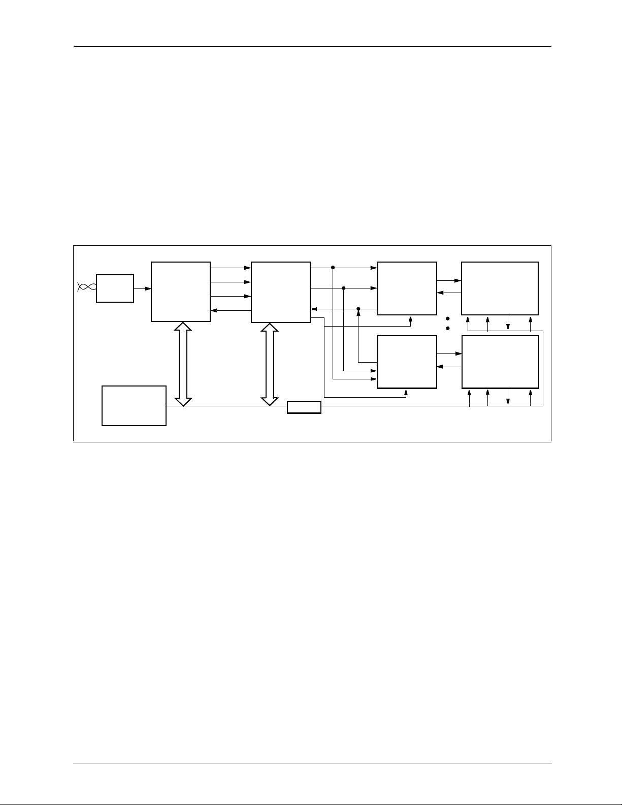
Bt8954’s position among the key elements of a PCM4 (4-channel) voice pair
gain modem is illustrated in Figure 1-1. The Pulse Code Multiplexed (PCM)
codec and Subscriber Line Interface Circuit (SLIC) chips for each channel
perform the transmit encoding (A/D conversion) and receive decoding (D/A
conversion) of voice signals. The time-division multiplexing of the voice signals
on the PCMT and PCMR serial buses is as follows: Bt8954 informs PCM
Codec_n with the PCMFn frame sync when to expect the next byte from Bt8954
on the PCMR bus, and when to put its next byte on the PCMT bus. In this way,
Bt8954 uses the PCMFn frame sync to designate the time slot that Codec_n has
access to the PCMR and PCMT buses.
Figure 1-1. Block Diagram of a PCM4 Voice Pair Gain Modem
QCLK
BCLK
RDAT
TDAT
Bt8954
VPG Framer
Hybrid
Bt8960/70
Bit Pump
PCMCLK
PCMR
PCMT
CODEC1
FSX1/FSR1
PCMF1
Voice Pair Gain Framer
SLIC1
C1 C2 DET* E0
.
Microcomputer
1.1.1 Repeaters
CODEC4
FSX4/FSR4
PCMF4
Logic
SLIC4
C1 C2 DET* E0
Figure 1-2 illustrates a pair of Bt8954 repeaters placed in line between Central
Office and remote terminals to extend the transmission distance. For each Bt8954
repeater, the BCLK/QCLK is connected to the BCLK/QCLK of its source
transceiver while the BCLK_REP/QCLK_REP is connected to the BCLK/QCLK
of its destination transceiver. The Central Office Bt8954 gets its
HCLK/BCLK/QCLK from the Central Office transceiver, which generates them
from a free-running crystal. The repeater transceiver connected to the Central
Office recovers its HCLK, BCLK, and QCLK from the HDSL line. These signals
then drive the HCLK, BCLK, and QCLK pins of the Central Of fice to Remote
Terminal Bt8954, and the HCLK, BCLK_REP, and QCLK_REP pins of the
Remote Terminal to Central Office Bt8954. The repeater transceiver connected to
the Remote Terminal receives HCLK from the repeater transceiver connected to
the Central Office. The repeater transceiver connected to the Remote Terminal
generates BCLK/QCLK and drives the BCLK/QCLK pins of the Remote
Terminal to Central Office Terminal Bt8954. The repeater transceiver drives the
BCLK_REP/QCLK_REP pins of the Central Office Terminal to Remote
Terminal Bt8954.
1-2
In Repeater Mode, the Bt8954 does not use the FIFOs. First, data received
from the bit pump is descrambled.
Conexant
N8954DSC
Page 13
Bt8954
1.0 DSL Systems
Voice Pair Gain Framer
registers. The CRC is then calculated and inserted. Then the data is scrambled and
transmitted to the destination bit pump.
descrambles like Bt8954 in the remote terminal. That is, SCRAM_TAP = 0
[TCMD2; 0x87.1] but DSCRAM_TAP = 1 [RCMD_2; 0x91.4].
like Bt8954 in the Central Office terminal. That is, SCRAM_TAP = 1
[TDMD2; 0x87.1] but DSCRAM_TAP = 0 [RCMD_2; 0x91.4].
Figure 1-2. Repeater Block Diagram
Central Office Terminal
Bt8954
TDAT
RDAT
Bt8960/
Bt8970
1.1 Voice Pair Gain Applications
Next, EOC and IND overhead are inserted from the Bt8954 EOC and IND
Bt8954 (C→R) scrambles like Bt8954 in the Central Office terminal but
Bt8954 (R→C) scrambles like Bt8954 in the remote terminal but descrambles
Repeater
Bt8954 (C→R)
Bt8960/
Bt8970
BCLK
QCLK
RDAT TDAT
HCLK
BCLK_REP
QCLK_REP
Bt8960/
Bt8970
Remote Terminal
Bt8960/
Bt8970
Bt8954
RDAT
TDAT
XTAL
XTAL
Bt8954 (R→C)
TDAT
QCLK_REP
BCLK_REP
RDAT
QCLK
BCLK
XTAL
N8954DSC
Conexant
1-3
Page 14
1.0 DSL Systems
Bt8954
1.1 Voice Pair Gain Applications
1.1.2 Subscriber Modem
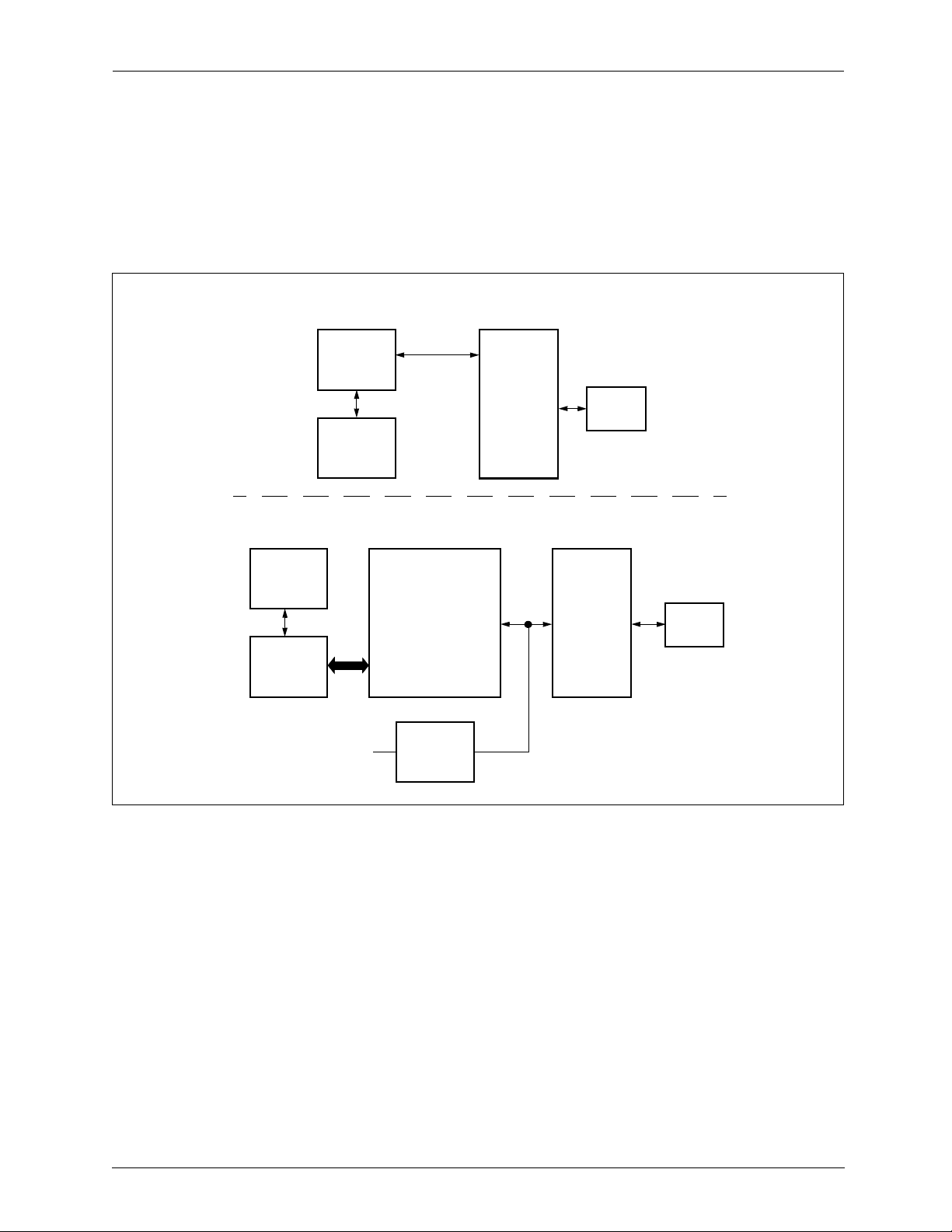
Figure 1-3 illustrates a DSL data modem application where a Central Processing
Unit (CPU) delivers PCM data directly to Bt8954. Alternatively, a multichannel
communications controller such as Bt8472/4 can be used to manage the transfer
of data between the CPU and the PCM channel through a local shared memory.
Figure 1-3. Subscriber Modem (Terminal) System Block Diagram
Single Channel Payload
CPU
PCM Serial
Port
Bt8954
Memory
Multichannel Payload
Voice Pair Gain Framer
Bit Pump
CPU
Shared
Memory
PCI
Bt8472/4
HDLC Controller
CODECPOTS
PCM
Bt8954
Bit Pump
1-4
Conexant
N8954DSC
Page 15
Bt8954
1.0 DSL Systems
Voice Pair Gain Framer
1.2 System Interfaces
System interfaces and associated signals for the Bt8954 functional circuit blocks
are illustrated in Figure 1-4. Circuit blocks are described in the following
sections, and signals are defined in Table 2-1.
Figure 1-4. Bt8954 System Interfaces
PCMT
ADPCMCK
PCMCKO
PCMCKI
PCMR
PCM
Interface
DSL
Interface
1.2 System Interfaces
BCLK_REP
QCLK_REP
BCLK
QCLK
TDAT
RDAT
PCMF[18:1]
HCLK
IRQ*
RST*
ADDR[7:0]
PLL
Microcomputer
Interface
CS*
AD[7:0]
ALE
RD*/DS*
WR*/R/W*
MOTEL*
MUXED
Test
Access
TCK
TDI
TDO
TMS
N8954DSC
Conexant
1-5
Page 16

1.0 DSL Systems
Bt8954
1.2 System Interfaces
Voice Pair Gain Framer
1-6
Conexant
N8954DSC
Page 17
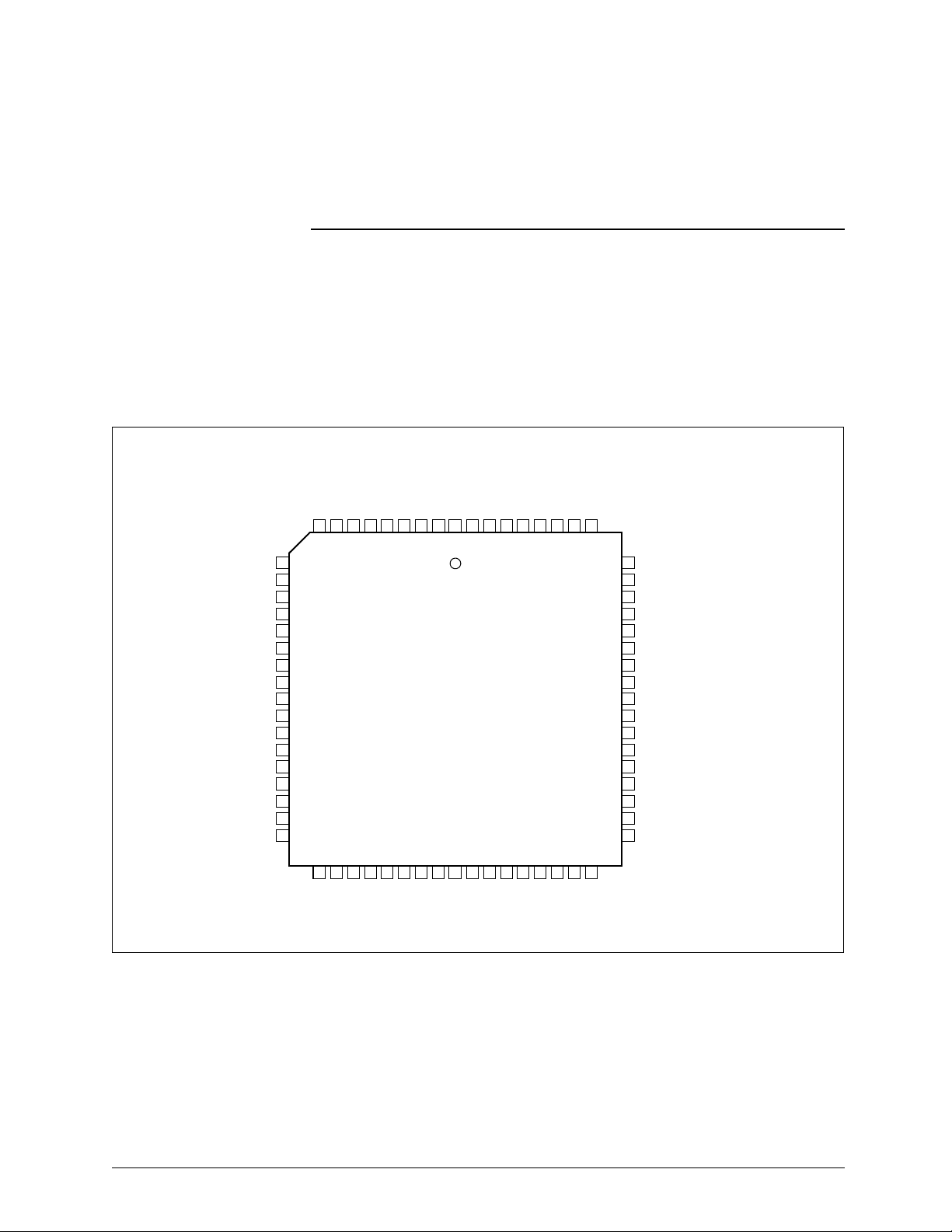
Figure 2-1. Pin Diagram
2
2.0 Pin Descriptions
Bt8954 pin assignments for the 68-pin Plastic Leaded Chip Carrier (PLCC)
package are illustrated in Figure 2-1. The functional pinout for the Bt8954 is
illustrated in Figure 2-2, and the signals are defined in Table 2-1.
QCLK
QCLK_REP
CS*
RD*/DS*
WR*/R/W*
ALE
ADDR[6]
VDD
GND
ADDR[5]
ADDR[4]
ADDR[3]
ADDR[2]
ADDR[1]
ADDR[0]
IRQ*
GND
10
11
12
13
14
15
16
17
18
19
20
21
22
23
24
25
26
HCLK
DTEST
8
9
28
27
VDD
AD[7]
BCLK_REP
BCLK
5
6
7
30
29
AD[5]
AD[6]
TDAT
RDAT
4
32
31
AD[3]
AD[4]
PLL_VDD
PCMF[18]
2
3
Bt8954
34
33
AD[1]
AD[2]
PCMF[16]
PCMF[17]
PLL_GND
1
67
68
37
36
35
AD[0]
MUXED
MOTEL*
PCMR
PCMF[14]
PCMF[15]
64
65
66
40
39
38
TCK
TDO
RST*
PCMCKO
PCMCKI
VDD
61
62
63
43
42
41
TDI
TMS
GND
60
ADPCMCK
59
PCMF[13]
58
PCMF[12]
57
PCMF[11]
56
PCMF[10]
55
PCMF[9]
54
VDD
53
GND
52
PCMF[8]
51
PCMF[7]
50
PCMF[6]/EPCMF[6]
49
PCMF[5]/EPCMF[5]
48
PCMF[4]/EPCMF[4]
47
PCMF[3]/EPCMF[3]
46
PCMF[2]/EPCMF[2]
45
PCMF[1]/EPCMF[1]
44
PCMT
N8954DSC
Conexant
2-1
Page 18
2.0 Pin Descriptions
Bt8954
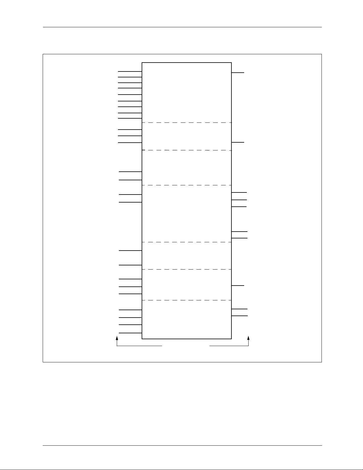
Figure 2-2. Bt8954 Functional Pinout
Motorola/Intel
Write*/Read/Write
Address Latch Enable
Interrupt Request
Address Data
Reset
Chip Select
Read/Data Strobe
Quaternary Clock
Receive Data
Bit Clock
BCLK Repeater
QCLK Repeater
PCM Transmit Data Input
PCM Clock Input
I
I
I
I
I/O
16, 19-24
I
I
I
I
I
I
I
I
I
I
I
36
14
15
37
28-35
38
12
13
10
5
6
7
11
43
63
MOTEL*
WR*/R/W*
ALE
MUXED
AD[7:0]
ADDR[6:0]Address Bus
RST*
CS*
RD*/DS*
QCLK
RDAT
BCLK
BCLK_REP
QCLK_REP
PCMT
PCMCKI
Microcomputer
Interface
DSL Interface
Repeater Pins
PCM Interface
IRQ* Interrupt Request
TDAT
PCMCKO
ADPCMCK
PCMR
PCMF[18:1]
EPCMFn[6:1]
25
4
62
59
64
44-51
54-58
65-68,3
44-49
Voice Pair Gain Framer
OD
O
Transmit Data
PCM Clock Output
O
ADPCM Clock Output
O
O
PCM Receive Data Output
PCM Frame Sync
O
PCM Frame SyncO
HCLK Input
Digital Test
JTAG Test Data In
JTAG Test Mode Select
Power Supply
Power Supply
8
I
I
I
I
I
HCLK
9
DTEST
41
TDI
42
TMS TDO JTAG Test Data Out
39
TCKJTAG Test Clock
61, 27
VDD
17, 53
VDD
2
PLL_VDDPLL Power Supply
1
PLL_GNDPLL Ground
I/O = Bidirectional, OD = Open Drain
Test and Diagnostic
I = Input, O = Output,
PLL
Interface
Power and
Ground
GND_O
GND_IC
40
26, 60
18, 52
O
Ground
GroundI
2-2
Conexant
N8954DSC
Page 19

Bt8954
2.0 Pin Descriptions
Voice Pair Gain Framer
Table 2-1. Hardware Signal Definitions
Pin Label
MOTEL* 36 Motorola/Intel* I Selects between Motorola and Intel hands hake conventions
ALE 15 Address Latch Enable I Falling-edge-sensitive input. The value of AD[7:0] when
CS* 12 Chip Select I Active-low input used to enable read/write operations on the
RD*/DS* 13 Read/Data Strobe I Bimodal input for controlling read/write access on the MCI.
Pin
Number
(1 of 4)
Signal Name I/O Definition
for the RD*/DS* and WR*/R/W* signals.
MOTEL* = 1 for Motorola protocol: DS*, R/W*;
MOTEL* = 0 for Intel protocol: RD*, WR*.
MUXED = 1, or of ADDR[7:0] when MUXED = 0, is internally
latched on the falling edge of ALE.
Microcomputer Interface (MCI).
When MOTEL* = 1 and CS* = 0, RD*/DS* behaves as an
active-low data strobe, DS*. Internal data is output on
AD[7:0] when DS* = 0 and R/W* = 1. External data is
internally latched from AD[7:0] on the rising edge of DS*
when R/W* = 0.
When MOTEL* = 0 and CS* = 0, RD*/DS* behaves as an
active-low read strobe RD*. Internal data is output on
AD[7:0] when RD* = 0. Write operations are not controlled
by RD* in this mode.
WR*/R/W* 14 Write/Read/Write I Bimodal input for controlling read/write access on the MC I.
When MOTEL* = 1 and CS* = 0, WR*/R/W* behaves as a
read/write select line, R/W*. Internal data is output on
AD[7:0] when DS* = 0 and R/W* = 1. External data is
internally latched from AD[7:0] on the rising edge of DS*
when R/W* = 0.
When MOTEL* = 0 and CS* = 0, WR*/R/W* behaves as
an active-low write strobe, WR*. External data is internally
latched from AD[7:0] on the rising edge of WR*. Rea d
Microcomputer Interface (MCI)
AD[7:0] 28–35 Address-Data[7:0] I /O Eight-bit bidirectional multiplexed address-data bus.
ADDR[6:0] 19–24, 16Address Bus [6:0]
(Not Multiplexed)
MUXED 37 Addressing Mo de Select I Controls the MCI addressing mode.
IRQ* 25 Interrupt Request O,ODActive-low open-drain output that indicate requests for
operations are not controlled by WR* in this mode.
AD[7] = MSB, AD[0] = LSB. Usage is controlled using the
MUXED signal.
I Provides a glueless interface to microcomputers with
separate address and data buses. ADDR[6] = MSB, ADDR[0]
= LSB. Usage is controlled using the MUXED signal.
When MUXED = 1, the MCI uses AD[7:0] as a multiplexed
signal for address and data (typical of Intel processors).
When MUXED = 0, the MCI uses ADDR[7:0] as the
address input and AD[7:0] for data only (typical of Motorola
processors).
interrupt. Asserted whenever at least one unmasked interrupt
flag is set. Remains inactive whenever no unmasked
interrupt flags are present.
RST* 38 Reset I Asynchronous, active-low, level-sensitive input that resets
the framer .
N8954DSC
Conexant
2-3
Page 20

2.0 Pin Descriptions
Bt8954
Table 2-1. Hardware Signal Definitions
Pin Label
BCLK 6 Bit Clock I Corresponds to the DSL channel. BCLK operates at the 2B1Q
QCLK 10 Quaternary Clock I Operates at the 2B1Q symbol rate (1/2 bit rate) and identifies
DSL Interface
Pin
Number
(2 of 4)
Signal Name I/O Definition
symbol rate. The rising edge of BCLK outputs 2x TDAT. The
falling edge of BCLK samples QCLK at the RDAT input. (In
the repeater terminal, BCLK is the BCLK from the bit pump to
which RDAT is connected.)
NOTE(S):
The BCLK signal from the bit-pump to the channel unit
device is sensitive to overshoot and undershoot. The BCLK
sensitivity could cause bit-errors in the system . A 100 Ω
series terminating resistor might be required to help dampen
the overshoot and undershoot. The bit-pump line cards
include a 74HCT244 to drive the long traces through the
motherboard 96-pin connectors.
sign and magnitude alignment of both the RDAT and TDAT
serially encoded bit streams.
1 = magnitude bit. In the Repeater Terminal, BCLK is the
BCLK from the bit pump to which RDAT is connected.
Refer to Appendix A, page 81.
The falling edge of BCLK samples QCLK: 0 = sign bit;
Voice Pair Gain Framer
TDAT 4 Transmit Data O DSL transmit data output at the bit rate on the rising edge of
BCLK. Serially encoded with the 2B1Q sign bit aligned to the
QCLK low level and the 2B1Q magnitude bit aligned to the
QCLK high level.
RDAT 5 Receive Data I DSL receive data input sampled on the falling edge of BCLK.
The serially encoded 2B1Q sign bit is sampled when QCLK is
low, and the 2B1Q magnitude bit is sampled when QCLK is
high.
BCLK_REP 7 BCLK from destination
bit pump in a repeater
terminal
QCLK_REP 11 QCLK from destination
Repeater Pins
bit pump in a repeater
terminal
I BCLK from the bit pump to which the Bt8954 TDAT is
connected in a repeater terminal. It is used only in the
repeater mode and should be tied to VDD or GND in
non-repeater terminals.
I QCLK from the bit pump to which the Bt8954 TDAT is
connected in a repeater terminal. It is used only in the
repeater mode and should be tied to VDD or GND in
non-repeater terminals.
2-4
Conexant
N8954DSC
Page 21

Bt8954
2.0 Pin Descriptions
Voice Pair Gain Framer
Table 2-1. Hardware Signal Definitions
Pin Label
PCMCKO 62 PCM Clock Output O Outpu t P CM clock for sending and receiving bits from PCM
PCMCKI 63 PCM Clock Input I Sends and receives bits from PCM codecs. Controls the PCM
ADPCMCK 59 ADPCM Clock Output O Used by ADPCM chips. It is 10x or 4x PCMCKO.
PCMFn 3,
PCM Interface
EPCMFn 44-49 Encoded PCM Frame
Pin
Number
44-51,
54-58,
65-68
PCM Frame Sync (n =
1,...,18)
Sync
(n = 1,...,6)
(3 of 4)
Signal Name I/O Definition
codecs. It is generated by the PLL and is 1.536 MHz or
2.048 MHz depending on the PLL configu r ation. Connect to
receive/transmit bit clocks and receive/transmit master
clocks of PCM codecs. In normal operation, tie to PCMCKI.
Formatter, reads from the RFIFO, and writes into the TFIFO.
In normal operation, tie to PCMCKO.
O Frame sync pulse for receiving bits from and transmitting
bits to a PCM codec. Connect to receive/transmit frame
syncs of the PCM codec. This signal is low if not connected
to any PCM codec. It supports both short-frame and
long-frame operations.
O Channel number of bits received from and transmitte d to
PCM codecs. Connect to a decoder to generate
receive/transmit frame syncs for PCM codecs. For n = 1,..,6,
EPCMFn is multiplexed with PCMFn depending on the
ENC_FSYNC configuration in the PCM Format register
[PCM_FORMAT; 0xF1.6].
PCMR 64 PCM Receive Data
Output
PCMT 43 PCM Transmit Data
Input
HCLK 8 HCLK Input I Connects to the HCLK output of the Bt8960/70 bit pump. It is
PLL
DTEST 9 Digital Test I DTEST–Active high test input used by Conexant to enable an
O Serial bit stream to PCM codecs is shifted out at the rising
edge of PCMCKI.
I Serial bit stream from the PCM codecs is sampled at the
falling edge of PCMCKI.
32xBCLK or 64xQCLK and is used as the PLL clock
reference.
internal test mode. This input should be tied to ground
(GND).
N8954DSC
Conexant
2-5
Page 22

2.0 Pin Descriptions
Bt8954
Table 2-1. Hardware Signal Definitions
Pin Label
TDI 41 JTAG Test Data Input I Test data input per IEEE Std 1149.1-1990. Used for loading
TMS 42 JTAG Test Mode Select I Test mode select input per IEEE Std 1149.1-1990. Internally
TDO 40 JTAG Test Data Output O Test data output per IEEE Std 1149.1-1990. Three-state
Test and Diagnostic Interface
TCK 39 JTAG Test Clock I Test clock input per IEEE Std 1149.1-1990. Used for all test
VDD 17,
Pin
Number
Power Supply I Power supply pins for the I/O buffers and core logic
27,
53,
61
(4 of 4)
Signal Name I/O Definition
all serial instructions and data into internal test l ogi c.
Sampled on the rising edge of TCK. TDI can be left
unconnected if it is not being used because it is pulled up
internally.
pulled-up input signal that controls the test-logic state
machine. Sampled on the rising edge of TCK. TMS can be left
unconnected if it is not being used because it is pulled up
internally.
output used for reading all serial configuration and test data
from internal test logic. Updated on the falling edge of TCK.
interface and internal test-logic operations. If unus ed, TCK
should be pulled low.
functions.
5VDC±5%.
Voice Pair Gain Framer
GND 18,
26,
52,
60
Power and Ground
PLL_VDD 2 PLL Power Supply P Dedicated supply pin for the PLL circuitry. Connect to VDD
PLL_GND 1 PLL Ground G Dedicated ground pin for the PLL circuitry. Must be held at
Ground G Ground pins for the I/O buffers and core logic functions.
Must be held at the same potential as PLL_GND.
externally.
the same potential as GND.
2-6
Conexant
N8954DSC
Page 23
3
3.0 Circuit Descriptions
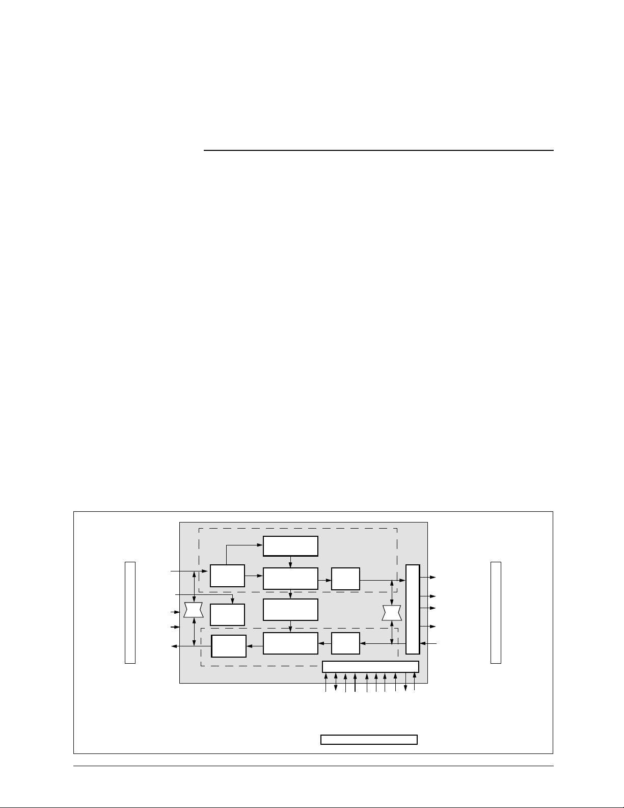
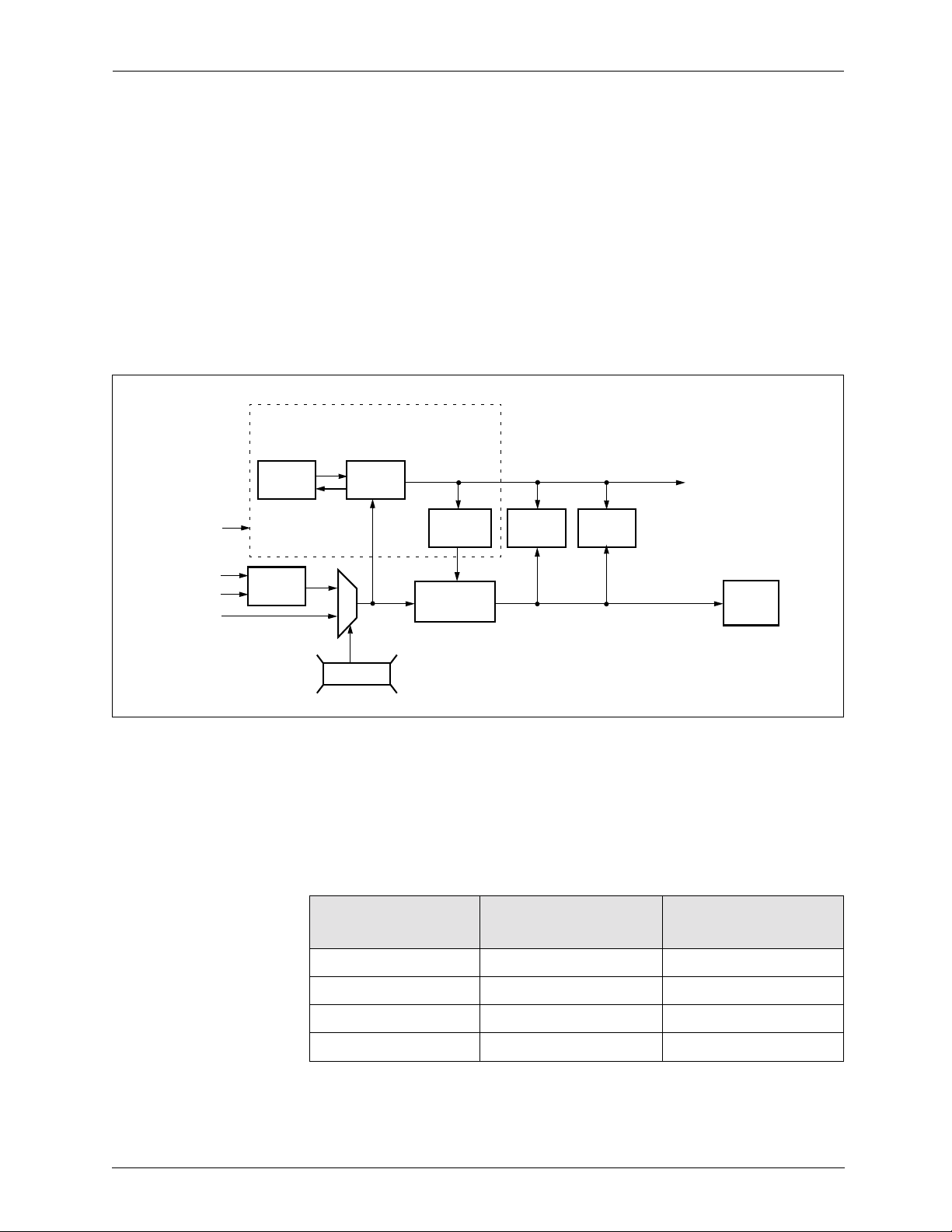
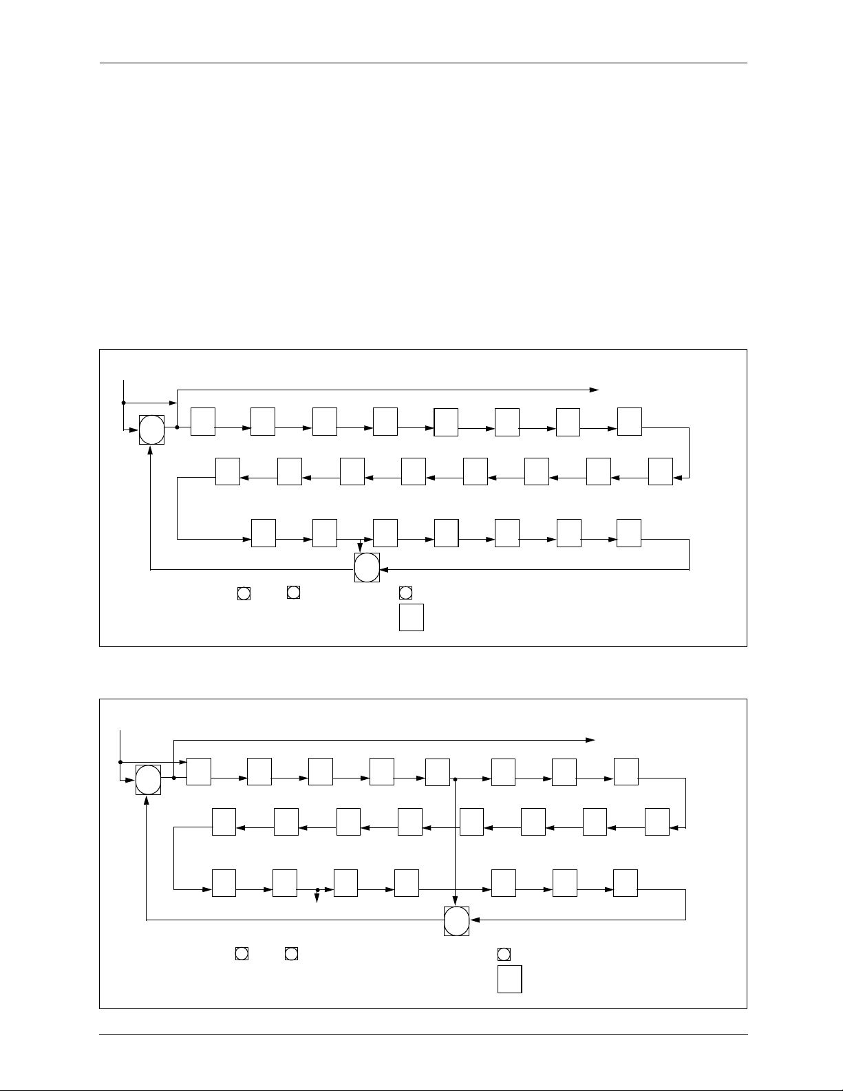
3.1 Overview
Figure 3-1 details the major blocks and pins of Bt8954. After the 2B1Q decode of
the bit stream is received from the DSL bit pump, the Receive Framer detects the
beginning of the Digital Subscriber Line (DSL) frame, and generates the required
pulses for synchronizing the different demultiplexing functions. The Payload
Demux block strips overhead bits from the DSL frame and puts the payload for
the different Pulse Code Multiplexed (PCM) time slots into the PCM RFIFO.
The PCM RFIFO is emptied through the PCMR pin.
On the transmit side, the PCM TFIFO is filled with serial data on PCMT.
Payload data from the TFIFO is multiplexed with signaling data from the
signaling registers and overhead from the OH (overhead) registers. The
multiplexed data is then sent to the DSL bit pump, through the TDAT pin, after
being 2B1Q encoded.
PCM and DSL loopback functions are performed using the loopback blocks.
The PCMCLK, ADPCMCK, and the internal clock are generated and
synchronized to BCLK with the PLL. The PLL uses HCLK as its clock reference.
Figure 3-1. Block Diagram
RDAT
HCLK
BCLK
QCLK
DSL Bit-Pump
TDAT
N8954DSC
Receiver
LB
Transmitter
2B1Q
Decoder
PLL
2B1Q
Encoder
Receive
Framer
Payload
Demux
OH/Signaling
Registers
Payload
Mux
Conexant
PCM
RFIFO
LB
PCM
TFIFO
Microcomputer Interface
CS*
DS*
ALE
AD[7:0]
MUXED
ADDR[7:0]
Microcomputer
WR/RW*
IRQ*
MOTEL*
PCM Formatter
RST*
PCMR
ADPCMCK
PCMCLK
PCMF[18:1]
PCMT
ADPCM/PCM Codecs
3-1
Page 24
3.0 Circuit Descriptions
Bt8954
3.2 DSL Frame Format
3.2 DSL Frame Format
The DSL frame is the fundamental data element of the bit streams transmitted and
received by Bt8954 at the DSL interface. It is patterned after the 2 T1, 2 E1, and
3 E1 frame structures. Figure 3-2 illustrates the basic format of a DSL frame.
Figure 3-2. Basic DSL Frame Format
0 ms
1Q
7Q
S
S
Sync
t
t
Word
q
q
1
2
D
B
O
0
H
1
12x(4N+0.5S)
B
0
2
DSL Frame
#Quats = 4 x (48N + 6S) + 24 = 192N + 24S + 24
#Bits = 2 x (192N + 24S + 24)
Bit Rate (kbps) = 2 x (192N + 24S + 24)
5Q
B
D
B
1
2
B
O
1
1
H
3
4
6 ms
5Q 5Q
B
D
B
2
O
2
4
H
5
= (64N + 8S + 8)
B
2
6
Voice Pair Gain Framer
6 ms
1Q1Q
S
B
D
B
3
6
B
O
3
3
H
7
8
S
B
4
8
Sync
t
t
Word
q
q
1
2
1/(32N + 4S + 4) ms
S-Bits Byte1 Byte2 Byte3 Byte_N
0-8 Bits 8 Bits
3.2.1 Detailed Frame Structure
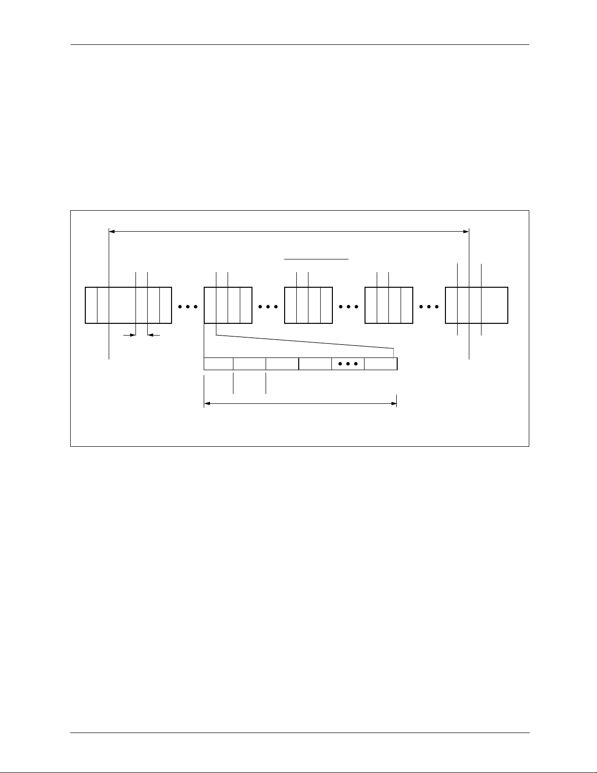
Each frame has a 6 ms duration and is made up of 48 payload blocks. Each block
contains S number of S-bits (for data signaling) and N number of bytes where N
is the number of PCM time slots. The microcomputer selects the number of S-bits
in the NUM_SBITS [3:0] field of Transmit Command register 2
[TCMD_2; 0x87.5:2] and the N number of PCM time slots in the NUM_
CHAN[4:0] field of the PCM Format register [PCM_FORMAT; 0xF1.4:0]. S-bits
vary from 0 to 8 bits, while N varies from 1 to 18 time slots. Groups of 12 payload
blocks are concatenated, and each group is separated by an ordered set of DOH
(DSL ov erhead) bits. A 14-bit SYNC word pattern identifies the beginning of the
DSL frame.
Forty-eight overhead bits are defined in one DSL frame with the last 2 bits
used for stuffing. This corresponds to an 8 kbps (48 bits/6 ms) overhead bit rate.
The 2 bits of stuffing are the average number of stuffing bits per frame since the
transmitter alternatively transmits 0 bits of stuffing or 4 bits of stuffing in each
frame.
Bnn
#Quats = (4N + 0.5S)
#Bits = 2 x (4N + 0.5S)
“6+”“6-”
LEGEND:
Bnn = Payload Blocks 1-48
DOH = DSL Overhead
S-bits = Data Signaling Bits
N = # of Voice Channels
3-2
Conexant
N8954DSC
Page 25
Bt8954
3.0 Circuit Descriptions
Voice Pair Gain Framer
3.2.2 Differences Between the DSL and HDSL T1/E1 Frame Formats
The DSL frame format is similar to the T1/E1 frame formats that are transported
on one HDSL loop. The main difference is due to the number of S-bits. While
fixed as 1 F-bit/block and 1 Z-bit/block for the T1 and E1 HDSL frame f ormats, it
can vary between 0 and 8 bits for the DSL frame format. The number of S-bits is
allow e d to v ary up to 8 bits so that a v ariab le numb er of D-channel bit r ates (up to
64 kbps) can be supported.
3.2.2.1 EXTRA_Z_BIT Option
Some systems (e.g., PCM11) require an extra 8 kbps Z-bit field in addition to the
basic frame structure outlined in Figure 3-2. T o accommodate such systems, each
block of the DSL frame has an extra Z-bit (preceding the S-bits field) that can be
enabled for transmit when EXTRA_Z_BIT in Command register 1
[CMD_1; 0xC0.5] is set. For example, a PCM11 system can have a 784 kbps bit
rate consisting of 704 kbps (11x64 kbps) of payload, 8 kbps of ov er head, 64 kbps
of signaling information, and 8 kbps of the extra Z-bit. This extra Z-bit field is a
dummy field and is not accessible through the MC.
3.2.3 Overhead Bit Allocation
The overhead bit allocation of the DSL frame is the same as that of the HDSL
frame given in Table 3-1.
3.2 DSL Frame Format
Table 3-1. DSL Frame Structure and Overhead Bit Allocation
DOH Bit
Number
1–14 SW1–SW14 SYNC Word —
15 losd Loss of Signal IND[12]
16 febe Far End Block Error IND[11]
17–20 eoc1–eoc4 Embedded Operations Channel EOC[12]–EOC[9]
21–22 crc1–crc2 Cyclic Redundancy Check —
23 ps1 HTU-R Power Status IND[10]
24 ps2 Power Status Bit 2 IND[9]
25 bpv Bipolar Violation IND[8]
26 eo c5 Embedded Operations Channel EOC[8]
27–30 eoc6–eoc9 Embedded Operati ons Channel EOC[7]–EOC[4]
31–32 crc3–crc4 Cyclic Redundancy Check —
33 hrp HDSL Repeater Present IND[7]
Symbol Bit Name DOH Register Bit
Payload Blocks 1–12
Payload Blocks 13–24
(1 of 2)
N8954DSC
34 rrbe Repeater Remote Block Error IND[6]
35 rcbe Repeater Central Block Error IND[5]
36 rega Repeater Alarm IND[4]
Conexant
3-3
Page 26
3.0 Circuit Descriptions
Bt8954
3.2 DSL Frame Format
Voice Pair Gain Framer
Table 3-1. DSL Frame Structure and Overhead Bit Allocation
DOH Bit
Number
37–40 eoc10–eoc13 Embedded Operations Channel EOC[3]–EOC[0]
41–42 crc5–crc6 Cyclic Redundancy Check —
43 rta Remote Terminal Alarm IND[3]
44 rtr Ready to Receive IND[2]
45 uib Unspecified Indicator Bit IND[1]
46 uib Unspecified Indicator Bit IND[0]
Symbol Bit Name DOH Register Bit
Payload Blocks 25–36
Payload Blocks 37–48
(2 of 2)
3-4
Conexant
N8954DSC
Page 27
Bt8954
3.0 Circuit Descriptions
Voice Pair Gain Framer
3.3 Receiver
The receiver performs SYNC word detection, overhead extraction, descrambling
of payload data, error performance monitoring, and payload mapping of DSL data
from the received DSL frame into the PCM RFIFO. Figure 3-3 illustrates the
receiver block diagram. The receiver consists of the 2B1Q decoder, receive
framer, descramb ler, CRC check, and payload demux.
Figure 3-3. Receiver Block Diagram
Receive Framer
State
CNT
BCLK
Sync
Detector
STUFF
Detector
CRC
CHK
3.3 Receiver
RDSL_6ms
Payload
Demux
QCLK
RDAT
TDAT
2B1Q
Decoder
3.3.1 2B1Q Decoder
0
1
PD_LOOP
Descrambler
RDAT_DESCR
PCM
RFIFO
The 2 Binary, 1 Quaternary (2B1Q) decoder provides the capability to connect
directly to the Bt8960/70 DSL transceivers. The 2B1Q decoder samples and
aligns the incoming sign and magnitude data. Refer to Table 3-2 for 2B1Q
mapping.
Table 3-2. 2B1Q Decoder Alignment
First Bit
(Sign)
10+3
11+1
01–1
Second Bit
(Magnitudes)
Quaternary Symbol
(Quat)
N8954DSC
00–3
Conexant
3-5
Page 28
3.0 Circuit Descriptions
Bt8954
3.3 Receiver
3.3.2 Receive Framer
Voice Pair Gain Framer
The receive framer generates the RDSL_6ms pulse after detecting the SYNC
WORD. RDSL_6ms generates pointers that control overhead extraction in the
CRC and OH demux circuitry. The MC initializes the framer to the OUT_OF
SYNC state by writing an y data value to SYNC_RST [0xD8]. F rom the OUT_OF
SYNC state, the framer advances to SYNC_A CQUIRED when the SYNC w ord is
detected. The framer searches all bits received on RDAT to locate a match with
the SYNC word pattern, SYNC_WORD [0xA1].
Due to the possibility of Tip/Ring connector reversal, all sign bits received on
RDAT might be inverted. Therefore, the receive framer searches for both the
programmed SYNC word value and the sign-inverted SYNC word value.
Consequently, a maximum of two values of the SYNC word are used in finding
the frame location. If the SYNC word detected is a sign-in verted version of the
configured SYNC word, the framer sets the Tip/Ring Inversion [TR_INVERT]
status bit of the Receive Status 1 register [RSTATUS_1; 0xE5.6] and
automatically inverts the sign of all quats received on RDAT.
After detecting the SYNC WORD and changing to the SYNC_ACQUIRED
state, the framer progresses through a programmable number of intermediate
SYNC_ACQUIRED states before entering the IN_SYNC state. In each
SYNC_ACQUIRED state, the framer searches for the previously detected SYNC
word v alue in one of tw o locations based upon the absence or presence of the four
STUFF bits (detected by the STUFF Detector). If the SYNC word is detected in
one of the two possible locations, the STATE_CNT[2:0] counter is incremented
[RSTATUS_2; 0xE6.2:0]. When STATE_CNT[2:0] increments to the value
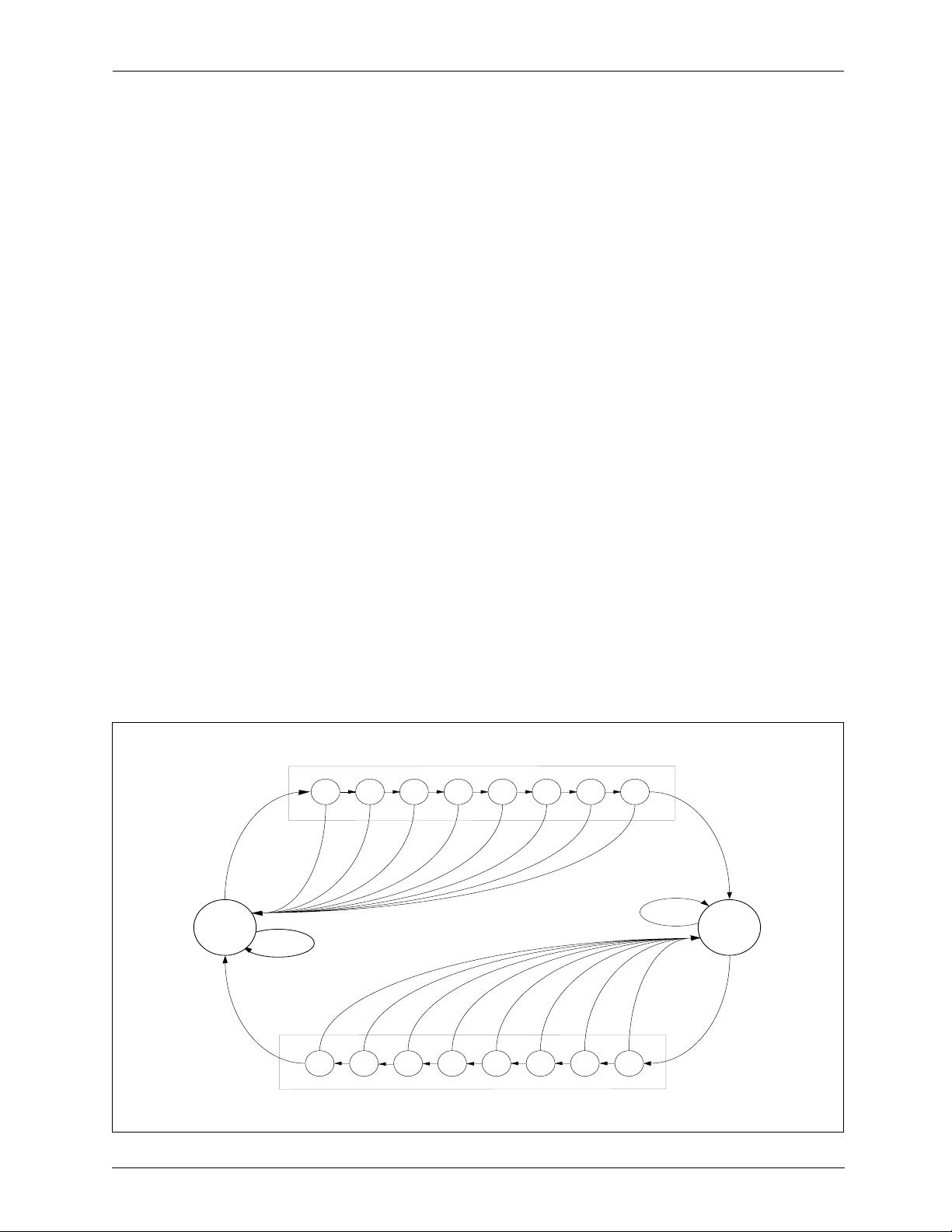
selected by the REACH_SYNC[2:0] criteria [RCMD_1; 0x90.2:0], the framer
changes to the IN_SYNC state. During the SYNC_ACQUIRED state, if valid
SYNC is not detected at one of the two possible locations, the framer returns to
the OUT_OF_SYNC state as illustrated in Figure 3-4.
Figure 3-4. Receive Framer Finite State Machine
Consecutive SYNC_ACQUIRED states per REACH_SYNC criteria
SYNC
NO SYNC
OUT_OF
SYNC
NO SYNC
NO
SYNC
87654321
Consecutive SYNC_ERRORED states per LOSS_SYNC criteria
87654321
SYNC
SYNC
IN_SYNC
SYNC
NO SYNC
3-6
Conexant
N8954DSC
Page 29
Bt8954
3.0 Circuit Descriptions
Voice Pair Gain Framer
After entering IN_SYNC, the framer either remains IN_SYNC as successive
SYNC words are detected or regresses to the SYNC_ERRORED state if SYNC
pattern errors are found. During SYNC_ERRORED states, the number of
matching bits from each comparison of received SYNC word and the
programmed SYNC word pattern must meet or exceed the programmed pattern
match tolerance specified by THRESH_CORR [RCMD_2; 0x91.3:0]. If the
number of matching bits falls below tolerance, the framer expands the locations
searched to quats on either side of the expected location, as illustrated in
Figure 3-5. After detecting a SYNC pattern error and changing to the
SYNC_ ERRORED state, the framer passes through a programmable number of
intermediate SYNC_ERRORED states, before entering the OUT_OF SYNC
state. STATE_CNT increments for each frame in which SYNC is not detected
until the count reaches the LOSS_SYNC[2:0] criteria [RCMD_1; 0x90.5–3] and
the framer enters the OUT_OF SYNC state. If at any time during the
SYNC_ERRORED state the framer detects a completely correct SYNC word
pattern at one of the valid frame locations, then framer returns to the IN_SYNC
state. The ETSI standard, for HDSL transport, recommends the
REACH_SYNC = 2 and LOSS_SYNC = 6 framing criteria.
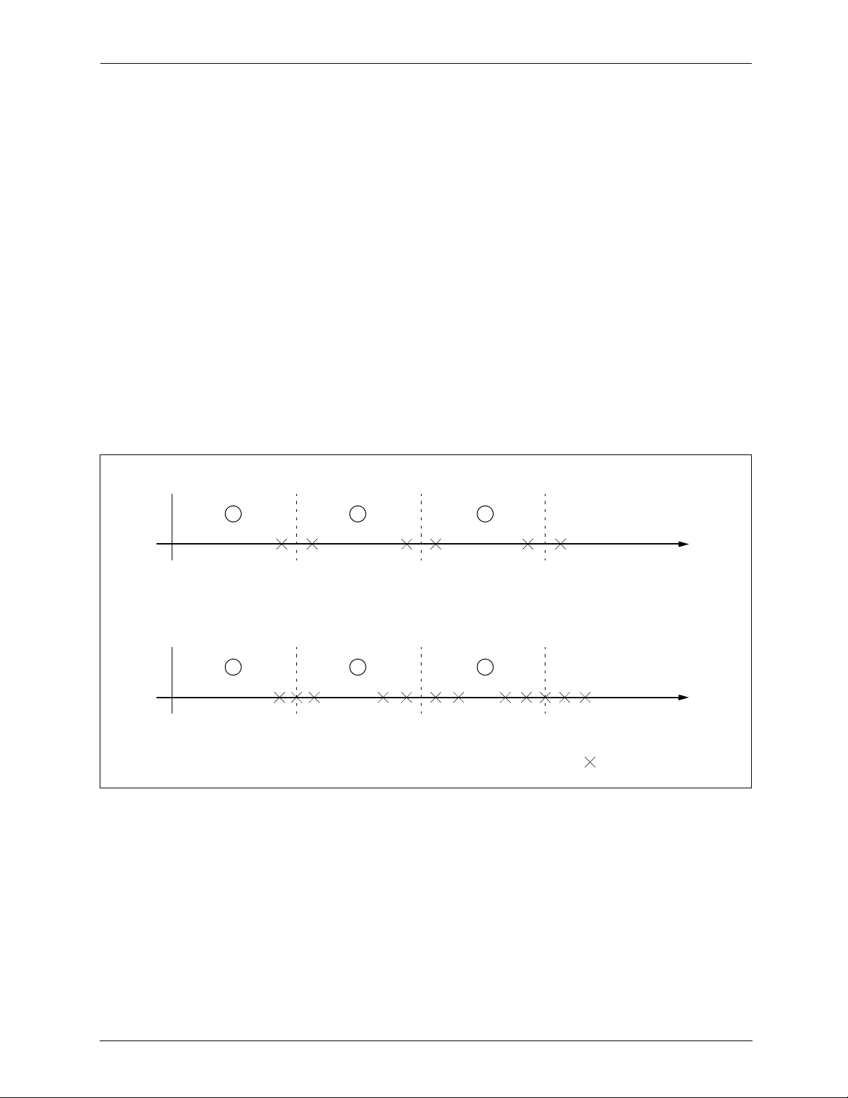
Figure 3-5. Threshold Correlation Effect on Expected SYNC Locations
3.3 Receiver
SYNC Pattern ≥ THRESH_CORR
SYNC_ERRORED
SYNC Pattern < THRESH_CORR
SYNC_ERRORED
3.3.3 CRC Check
SYNC_ERRORED
1
–1q +1q –1q +1q –1q +1q
6 ms 12 ms 18 ms0
SYNC_ERRORED
1
–2q +2q –1q +1q –2q +2q
6 ms 12 ms 18 ms0
2
2
–3q +3q +4q–4q
SYNC_ERRORED
SYNC_ERRORED
The CRC Check block calculates a CRC value for every receiv ed DSL frame. The
CRC Check block reports an error if the CRC in the current frame (calculated at
the other end’s transmitter) does not match the CRC that was calculated for the
previous DSL receive frame. Individual DSL block errors are reported in the
CRC_ERROR bit of the Receive Status 2 register [RSTATUS_2; 0xE6.5] and
accumulated in the CRC Error Count register [CRC_CNT; 0xE8]. The CRC
calculation in the receiver is exactly the same as that in the transmitter.
3
t
3
t
q = 2 bits = 1 quat
= Search Location
N8954DSC
Conexant
3-7
Page 30
3.0 Circuit Descriptions
Bt8954
3.3 Receiver
3.3.4 Descrambler
The MC enables the descrambler by setting DSCRAM_EN bit of the Receive
Command register and selects the descrambler algorithm via the DSCRAM_ TAP
[RCMD_2; 0x91.5,4]. The descrambler, if enabled, descrambles all DSL receive
data except the SYNC word. The algorithm is chosen from one of two possible
choices, depending on whether Bt8954 is located at the Central Office or at a
Remote Site.
The descrambler is basically a 23-bit-long Linear Feedback Shift register
(LFSR). The algorithm chosen determines the feedback points. The LFSR
structure and polynomials for the two descrambler algorithms are illustrated in
Figure 3-6 and Figure 3-7. The descrambler is clocked with BCLK.
Figure 3-6. LFSR Structure for Transmission in the Remote
Scrambled Input (bk)
x
-1
k-1
z
x
-1
k-2
z
x
-1
k-3
z
x
-1
z
+
x
k-16
x
-1
k-15
z
x
-1
k-14
z
x
-1
k-13
z
z
→
Central Office Direction
x
-1
z
k-12
x
k-5
-1
z
k-4
-1
z
x
-1
k-11
Voice Pair Gain Framer
Unscrambled Output (ck)
x
k-6
-1
z
z
x
-1
k-10
x
k-7
-1
z
x
-1
k-8
z
x
-1
k-9
z
x
-1
k-17
z
x
-1
k-18
z
x
-1
k-19
z
+
Polynomial: ck = xk-23
xk-18 b
+
Figure 3-7. LFSR Structure for Transmission in the Central Office
Scrambled Input (bk)
x
-1
z
k-1
-1
z
+
k
x
k-2
x
-1
k-3
z
+
= Modulo-2 Summation (XOR gate)
-1
= Delay Element (D flip-flop clocked with BCLK)
z
x
k-4
-1
z
-1
z
+
x
k-16
x
-1
k-15
z
x
-1
k-17
z
x
-1
k-14
z
x
-1
k-18
z
x
-1
k-13
z
x
-1
k-19
z
x
-1
k-12
z
-1
z
x
-1
k-20
z
→
Remote Direction
x
k-5
-1
z
x
k-20
z
x
z
-1
z
-1
k-11
-1
x
x
x
k-21
k-6
z
k-21
x
-1
k-22
z
Unscrambled Output (ck)
x
-1
k-7
z
x
-1
z
k-10
-1
x
z
k-22
-1
x
-1
k-23
z
x
-1
k-8
z
x
-1
k-9
z
x
-1
k-23
z
Polynomial: ck = xk-23
3-8
xk-5
+
b
+
k
Conexant
+
+
= Modulo-2 Summation (XOR gate)
-1
= Delay Element (D flip-flop clocked with BCLK)
z
N8954DSC
Page 31

Bt8954
3.0 Circuit Descriptions
Voice Pair Gain Framer
3.3.5 Payload Demux
3.3 Receiver
The Payload Demux block extracts the Indicator (IND), Embedded Operations
Channel (EOC), and the S-bits from each receive frame and places them in
microcomputer-accessible registers:
• Receive Indicator Bits [RIND 0xE2, 0xE3]
• Receive Embedded Operations Channel [REOC 0xE0, 0x61]
• Receive Signaling FIFOs [RSFIFO_O; 0xE4]
Double-buffering is u sed to ensure that the OH and signaling information read
by the microcomputer is not corrupted by newly arriving data. The
microcomputer must read the contents of the OH registers within 6 ms for every
frame; otherwise the data is overwritten with new received data. The
microcomputer must read the contents of the RSFIFO_O register within 6 ms, 3
ms, 2 ms, or 1 ms, depending on the EXTRA_SIG_UPDATE configuration bits
that are programmed in Command register 1 [CMD_1; 0xC0].
N8954DSC
Conexant
3-9
Page 32

3.0 Circuit Descriptions
Bt8954
3.4 Transmitter
3.4 Transmitter
The transmitter muxes payload data from the PCM channel with overhead and
signaling data into serially encoded 2B1Q data th at is sent to the bit pump through
the TDAT pin. Figure 3-8 details the transmitter block diagram, which consists of
Overhead (OH) registers, the Payload Mux, and the 2B1Q Encoder.
Figure 3-8. Transmitter Block Diagram
S-BIT
IND
EOC
PCM
TFIFO
4-level 1
CRC REG
CRC
OH/Signaling
Registers
Payload
MUX
1
Scrambler
0
SYNC
Word
1
0
Voice Pair Gain Framer
BCLK
QCLK
2B1Q
Encoder
TDAT
= Command Register Bit
3.4.1 OH/Signaling Registers
The OH/Signaling registers are the S-Bits, IND, EOC, CRC, and SYNC word
registers. Refer to the Overhead Bit Allocation section, Table 3-1, for the OH bit
positions in the DSL transmit frame. The OH/Signaling registers are accessible b y
the microcomputer for writing and reading.
RDAT_DESCR
DD_LOOP
Stuff
SCRAM_EN
3-10
Conexant
N8954DSC
Page 33

Bt8954
3.0 Circuit Descriptions
Voice Pair Gain Framer
3.4.2 Transmit Signaling FIFOs
Using two sets of transmit signaling FIFOs (TSFIFO_I and TSFIFO_O), double
buffering ensures that the MC has enough time to write new signaling
information without corrupting the signaling information being transmitted, as
illustrated in Figure 3-9.
Figure 3-9. Double Buffering, Using Transmit S-Bits Registers
Blocks In DSL Frame
TSFIFO Output Regs
LD_TSIG
TSFIFO Input Regs
LD_TSIG
Block1
S
Payload
TSFIFO_O[1]
TSFIFO_I[1] TSFIFO_I[48]TSFIFO_I[2]
Block2
S
Payload
TSFIFO_O[2]
LD
MC Loads TSFIFO_I REGS
Computer
µ
TSFIFO_I
TSFIFO_O
3.4 Transmitter
Block48
S
Payload
TSFIFO_O[48]
LDLD
→
Transmit TSFIFO_O REGS
DSL_SUBFRAME_N (6 ms, 3 ms, 2 ms, 1 ms) DSL_SUBFRAME_N+1 (6ms, 3ms, 2ms, 1ms)
3.4.3 Payload Mux
The MC loads the TSFIFO_I registers after receiving the LD_TSIG interrupt.
In the default case, LD_TSIG is the same as the DSL 6 ms receive frame interrupt
that occurs upon the arrival of the 6 ms DSL frame. The LD_TSIG interrupt can
be made to occur more frequently than 6 ms by programming non-00 values in
the EXTRA_SIG_UPDATE bits in the CMD_1 register [0xC0]. Six, three, two,
or one millisecond(s) later, TSFIFO_I registers are loaded into TSFIFO_O
registers at the next LD_TSIG. TSFIFO_O, which is then transmitted, is not
thereby corrupted by the new TSFIFO_I values being written by the MC during
the next interval.
The Payload Mux multiplexes the overhead bits from the OH registers, payload
data from the PCM TFIFO, the SYNC w ord and the CRC bits that were calculated
for the previous transmit frame.
N8954DSC
Conexant
3-11
Page 34

3.0 Circuit Descriptions
Bt8954
3.4 Transmitter
3.4.4 CRC Calculation
Voice Pair Gain Framer
The CRC calculation is performed on all transmit data, and the Payload Mux
inserts the resulting 6-bit CRC into the subsequent output frame. CRC is
calculated over all bits in the (N)th frame except the SYNC WORD, STUFF, and
CRC bits and then is inserted into the (N+1) frame. The MPU can choose to inject
CRC errors on a per-frame basis by setting the ICRC_ERR bit [TCMD_1;
addr 0x86.1]. The six CRC bits are calculated as follows:
1.
All bits of the (N) frame — except the 14 SYNC and 6 CRC bits, for a total
of M bits — are used in order of occurrence to construct a polynomial in X
M-1
such that bit 0 of the (N) frame is the coefficient of the term X
0
M-1 of the (N) frame is the coefficient of the term X
2.
The polynomial is multiplied by the factor X6, and the result is divided,
modulo 2, by the generator polynomial X
6
⊕X⊕1. Coefficients of the
.
and bit
remainder polynomial are used, in order of occurrence, as an ordered set of
check bits, CRC1–CRC6, for the (N+1) frame. Ordering is such that the
5
coefficient of term X
the coefficient of term X
3.
Check bits CRC1–CRC6 contained in a frame are associated with the
in the remainder polynomial is check bit CRC1, and
0
is check bit CRC6.
contents of the preceding frame. When there is no immediately preceding
frame, check bits may be assigned any value.
3.4.5 Scrambler
Figure 3-10.
Unscrambled Input (Bk)
LFSR Structure for Transmission in the Remote → Central Office Direction
-1
z
+
x
k-16
The MC enables the scrambler b y setting SCRAM_EN [TCMD_1; 0x86.0] and
selects the descrambler algorithm via SCRAM_TAP [TCMD_2; 0x87.2]. The
scrambler, if enab led , scrambles all DSL transmit data except the SYNC w ord and
STUFF bits. The algorithm is chosen from one of two possible choices,
depending on whether Bt8954 is located at the Central Office or at a Remote Site.
Scrambler Algorithms:
The scrambler is basically a 23-bit-long Linear
Feedback Shift register (LFSR). The algorithm chosen determines the feedback
points. The LFSR structure and polynomials for the two scrambler algorithms are
illustrated in Figure 3-10 and Figure 3-11.
Scrambled Output (ck)
x
z
k-14
z
x
-1
k-3
-1
z
x
-1
k-18
x
k-1
-1
z
x
z
k-15
z
x
-1
k-2
-1
z
x
-1
k-17
x
z
k-13
z
x
k-4
-1
-1
z
x
-1
k-19
x
-1
z
k-12
-1
z
x
x
k-5
z
k-20
-1
z
x
z
-1
k-11
-1
x
x
k-6
z
k-21
x
-1
k-7
z
x
-1
z
k-10
-1
x
z
k-22
-1
x
-1
k-8
z
x
-1
k-9
z
x
-1
k-23
z
Polynomial: ck = xk-23
3-12
+
xk-18
+
b
+
k
+
= modulo-2 summation (XOR gate)
-1
= Delay Element (D flip-flop clocked with BCLK)
z
Conexant
N8954DSC
Page 35

Bt8954
3.0 Circuit Descriptions
Voice Pair Gain Framer
Figure 3-11. LFSR Structure for Transmission in the Central Office → Remote Direction
Scrambled Input (bk)
x
-1
k-1
z
x
-1
k-2
z
x
-1
k-3
z
x
k-4
-1
z
x
-1
k-5
z
x
-1
k-6
z
z
+
x
k-16
x
-1
k-15
z
-1
z
x
z
k-17
x
-1
k-14
-1
z
x
z
k-18
x
-1
k-13
-1
z
x
-1
z
k-19
x
k-12
-1
z
x
z
k-20
x
-1
k-11
-1
z
z
x
-1
k-21
x
+
Polynomial: ck = xk-23
+ +
3.4.6 2B1Q Encoder
xk-5
b
k
+
= modulo-2 summation (XOR gate)
-1
= Delay Element (D flip-flop clocked with BCLK)
z
Unscrambled Output (ck)
x
-1
k-7
-1
k-10
z
x
-1
k-22
z
3.4 Transmitter
x
-1
k-8
z
x
-1
k-9
z
x
-1
k-23
z
The 2B1Q encoder converts the data to be transmitted to the bit pump into sign
and magnitude data according to the quaternary alignment provided on the QCLK
input. Table 3-3 depicts how sign and magnitude bits generate 2B1Q coded
outputs on TDAT.
Table 3-3. 2B1Q Encoder Alignment
First Input Bit
(Sign)
00–3
01–1
11+1
10+3
Second Input Bit
(Magnitude)
Quaternary Symbol
N8954DSC
Conexant
3-13
Page 36

3.0 Circuit Descriptions
Bt8954
3.5 PCM Formatter
Voice Pair Gain Framer
3.5 PCM Formatter
The PCM formatter shifts out the PCMR data at the rising edge of PCMCKI,
samples the PCMT data at the falling edge of PCMCKI, and generates the PCM
frame SYNC signals based on the PCM Format Configuration register [0xF1] as
illustrated in Figure 3-12. The PCM formatter supports direct connection to
popular PCM codecs. Because the formatter generates only one frame SYNC
signal for each PCM codec, codecs like the T e xas Instruments TP3054A that hav e
two frame SYNC signals (FSX for transmit and FSR for receive) must have both
frame SYNCs tied before being connected to the Bt8954.
Figure 3-12. PCM Formatter Detail
PCM
RFIFO
PCM
TFIFO
PCM Formatter
PCMR
ADPCMCK
PCMCKO
PCMCKI
PCMF[18:1]
PCMT
PCM Codecs
3-14
All time slots carry clear voice or compressed voice channels depending on
the COMPRESSED bit configuration in the PCM Format register [0xF1.5]. Only
2:1 ADPCM compression is allowed. Therefore, a 64 kbps time slot is carrying
either 2 x 32 kbps of compressed voice or 64 kbps or clear voice. The Bt8954 has
a maximum capacity of 18 clear or 36 compressed voice channels.
The frame SYNCs are in an encoded or decoded form depending on the
ENC_FSYNC bit configuration in PCM_FORMAT [0xF1.6]. If ENC_FSYNC is
reset, the PCM formatter can generate up to 18 frame SYNCs (PCMF[18:1]). In
this case, the frame SYNCs of all the unused time slots are held low. For e xample,
for a PCM4 system, PCMF[4:1] are active but PCMF[18:5] are held low.
If ENC_FSYNC is set, the PCM formatter generates the frame SYNCs in the
Encoded_Frame_SYNC mode, driving the channel numbers through
EPCMF[6:1], but holding PCMF[18:7] low. Externally, decoders can be used to
generate frame SYNCs from the channel numbers.
The period of PCMF[18:1] or EPCMF[6:1] for clear channels is 8 times the
PCMCKI period, while the period for compressed channels is 4 times the
PCMCKI period.
Conexant
N8954DSC
Page 37

Bt8954
3.0 Circuit Descriptions
Voice Pair Gain Framer
The PCMF[18:1] (EPCMF[6:1]) waveforms for various scenarios are
illustrated in Figure 3-13.
Figure 3-13. PCMF [18:1] Waveforms for Encoded and Decoded Frame SYNC Modes
1) PCM2: 2 Clear Channels
PCMCKI
(2.048 MHz)
PCMF1
PCMF2
PCMF[18:3]
30 Unused Timeslots
PCMT/
PCMR
2) PCM18: 18 Clear Channels
Time Slot 2Time Slot 1
BYTE1 BYTE2
3.9056µs
3.5 PCM Formatter
BYTE1
PCMCKI
(2.048 MHz)
PCMF1
PCMF18
PCMT/
PCMR
3) ADPCM36: 18 Compressed Channels
PCMCKI
(2.048 MHz)
EPCMF[6:1]
PCMF[18:7]
PCMT/
PCMR
BYTE1[7:4] BYTE1[3:0] BYTE18[7:4] BYTE18[3:0] BYTE1[7:4]
BYTE1 BYTE2 BYTE17 BYTE18
[00 0001] [00 0010]
125µs
[00 0011] [10 0010]
[0000 0000 0000]
BYTE2[7:4] BYTE17[3:0]
[10 0011]
[10 0100]
14 Unused
Time Slots
[00 0000]
BYTE1
[00 0001]
NOTE(S):
N8954DSC
SYNC_WIDTH (PCM_FORMAT_4) = 0001; FSYNC2BYTE (PCM_FORMAT_4) = 0001.
Conexant
3-15
Page 38

3.0 Circuit Descriptions
Bt8954
3.6 Loopbacks
3.6 Loopbacks
Bt8954 provides multiple PCM and DSL loopbacks as illustrated in Figure 3-14.
The output towards which data is looped is called the test direction. Loopback
activation in the test direction does not disrupt the through-data path in the
non-test direction. Table 3-4 lists the loopback controls which are designated by
initials corresponding to test direction and the channel from which data is looped.
Figure 3-14. PCM and DSL Loopbacks
DSL Channel
RDAT
DD_LOOP
TDAT
PD_LOOP
DP_LOOP
Voice Pair Gain Framer
PCM Channel
PCMR
PP_LOOP
PCMT
Table 3-4. PCM and DSL Loopbacks
Loopback Command Register Test Direction Loopback Description
PP_LOOP CMD_1; 0xC0 Receive PCM Loopback on PCM Side
DP_LOOP CMD_1; 0xC0 Transmit DSL Loopback on PCM Side
PD_LOOP RCMD_2; 0x91 Receive PCM Loopback on DSL Channel
DD_LOOP TCMD_2; 0x87 Transmit DSL Loopback on DSL Channel
3-16
Conexant
N8954DSC
Page 39

Bt8954
3.0 Circuit Descriptions
Voice Pair Gain Framer
3.7 Synchronization
3.7 Synchronization
All signals are synchronized to TDSL_6ms, RDSL_6ms, TPCM_6ms, and
RPCM_6ms. All status registers are synchronized to either TDSL_6ms or
RDSL_6ms. The transmitter signals at the DSL (PCM) interface are synchronized
to TDSL_6ms (TPCM_6ms). The receiver signals at the DSL (PCM) interface are
synchronized to RDSL_6ms (RPCM_6ms). The main contributor to the phase
differences between the DSL_6ms and PCM_6ms signals is that while data is
received and transmitted in a bursty fashion at the PCM interface, it is received
and transmitted in a continuous fashion at the DSL interface.
The detailed relationship between the DSL_6ms and PCM_6ms signals
depends on whether the framer is at the Central Office (COTF) or at the Remote
Site (RTF). Ev en though TPCM _6ms and RPCM_6ms may not be phase-aligned,
TFIFO and RFIFO prov ide sufficient data buffering for PCMF to mark coincident
PCM receive and transmit 125µs frame boundaries. The synchronization
between COTF and RTF is illustrated in Figure 3-15.
Figure 3-15. COTF and RTF Synchronization
COT Framer
TPCM_6 ms
(Master)
RPCM_6 ms
(Slave)
Transmitter.COT
Receiver.COT
TDSL_6 ms
(Slave)
Variable
RDSL_6 ms
(Master)
3.7.1 COTF Transmitter Synchronization
In the COTF, TPCM_6 ms is always a free-running 6 ms-period signal. At the
Central Office, the DSL transmit frames are slaved to the PCM frame timing. As
illustrated in Figure 3-16, TDSL_6 ms is a 6 ms-period signal that is phase-offset
from TPCM_6ms by TFIFO_WL.COT (TFIFO Water Level in the COTF).
TFIFO_WL.COT determines the amount of PCM data written into the TFIFO
before the transmitter begins extracting DSL frames from the TFIFO.
Figure 3-16. COTF Transmitter Synchronization
Path
Delay
RDSL_6 ms
(Master)
TDSL_6 ms
(Slave)
RT Framer
Receiver.RT
Transmitter.RT
RPCM_6 ms = TPCM_6 msRPCM_6 ms!= TPCM_6 ms
RPCM_6 ms
(Slave)
TPCM_6 ms
(Master)
TPCM_6 ms
TDSL_6 ms
N8954DSC
TFIFO_WL.COT
6 ms
Conexant
6 ms
3-17
Page 40

3.0 Circuit Descriptions
Bt8954
3.7 Synchronization
3.7.2 RTF Receiver Synchronization
The RDSL_6 ms signal in the RTF is generated after SYNC_WORD has been
detected on RDAT. As illustrated in Figure 3-17, RPCM_6 ms is phase-offset
from RDSL_6ms by RFIFO_WL.RT (RFIFO Water Level in the RTF). The PCM
receive frames are slaved to the DSL receive frame timing at the Remote Site.
Figure 3-17. RTF Receiver Synchronization
SYNC_WORD
RDAT
RDSL_6 ms
RPCM_6 ms
RFIFO_WL.RT
Voice Pair Gain Framer
SYNC_WORD
6 ms
6 ms
3.7.3 RTF Transmitter Synchronization
In the RTF, the RPCM_6 ms and TPCM_6 ms signals are the same because the
same PCM frame SYNC is used for transmitting and receiving PCM frames from
the PCM codecs. As illustrated in Figure 3-18, TDSL_6ms is phase-offset from
TPCM_6 ms by TFIFO_WL.RT (TFIFO Water Level in the RTF). The DSL
transmit frames are slaved to the PCM transmit frame timing, which in turn is
slaved to the DSL receive frame timing at the Remote Site.
TFIFO_WL.RT = TFIFO_WL.COT.
Figure 3-18. RTF Transmitter Synchronization
TPCM_6 ms
TDSL_6 ms
TFIFO_WL.RT = TFIFO_WL.COT
6 ms
6 ms
3-18
Conexant
N8954DSC
Page 41

Bt8954
3.0 Circuit Descriptions
Voice Pair Gain Framer
3.7.4 COTF Receiver Synchronization
The RDSL_6ms signal in the COTF is generated after SYNC_WORD has been
detected as illustrated in Figure 3-19. RPCM_6ms is phase-offset from
RDSL_6ms by RFIFO_WL.RT (RFIFO Water Level in the RTF) plus time to
realign to the next TPCM_125 µs. At the Central Office, the PCM receive frames
are slaved to the DSL frame timing and aligned to the transmit PCM_125 µs
frame. The re-alignment time is added because the same PCM frame SYNC
signal is used for transmitting and recei ving PCM frames from the PCM codecs.
Figure 3-19. COTF Receiver Synchronization
SYNC_WORD
RDAT
RDSL_6 ms
125 µs
TPCM_125 µs
RPCM_6 ms
3.7 Synchronization
SYNC_WORD
6 ms
125 µs
6 ms
RFIFO_WL.RT
3.7.5 Round Trip Delay
Realign to
TPCM_125 µs
The microcomputer determines the round-trip delay by measuring the time that
elapses between the Tx and Rx interrupts in the Interrupt Status register
[ISR; 0xD0] at the Central Office.
N8954DSC
Conexant
3-19
Page 42

3.0 Circuit Descriptions
Bt8954
3.8 Microcomputer Interface
Voice Pair Gain Framer
3.8 Microcomputer Interface
The microcomputer interface (MCI) port (Figure 3-20) configure s and controls
operating modes, manages overhead protocol, and reads status inform a tion from
Bt8954. In addition, Bt8954 may signal its need for attention from th e
microcomputer (MC) by requesting an interrupt. The port can be directly
connected to common MCs like the Motorola 68302 or the In tel 8051.
Figure 3-20. MCI Port
Microcomputer Interface
AD[7:0]
MUXED
ADDR[6:0]
Microcomputer
CS*
ALE
MOTEL*
WR/RW*
IRQ*
DS*
RST*
3-20
Conexant
N8954DSC
Page 43

Bt8954
3.0 Circuit Descriptions
Voice Pair Gain Framer
3.8.1 Microcomputer Read/Write
The MCI provides access to a 128-byte internal address space. Figure 3-21
depicts the read/write controls. The MCI uses either an 8-bit-wide multiplexed
address-data bus (Intel style) or one 8-bit-wide data bus and another separate
7-bit-wide address bus (Motorola style) for external data communications. The
interface is configured with the inputs, MOTEL* and MUXED. MOTEL* low
selects Intel-type microcomputer and control signals: ALE, CS*, RD*, WR*.
MOTEL* high selects Motorola-type microcomputer and control signals: ALE,
CS*, DS*, R/W*. MUXED high configures the interface to use the multiplexed
address-data bus with both the address and data on the AD[7:0] pins. MUXED
low configures the interface to use separate address and data buses with the data
on the AD[7:0] pins and the address on the ADDR[6:0] pins.
Figure 3-21. Functional Diagram of the Read and Write Controls
MUXED
MOTEL*
ALE
ADDR[7:0]
AD[7:0]
3.8 Microcomputer Interface
Address
To Registers
RD*/DS*
WR*/R/W*
CS*
3.8.1.1 Multiplexed Address/Data Bus
From Registers
Read Strobe
Write Strobe
The timing for a read or write cycle is stated in Chapter 5.0,
Mechanical Specifications
. During a read operation, an external microcomputer
Electrical and
places an address on the address-data bus which is then latched on the falling
edge of ALE. Data is placed on the address-data bus after CS* and RD* (or DS*)
go low. The read cycle is completed with the rising edge of CS* and RD* (or
DS*).
A write operation latches the address from the address-data bus at the falling
edge of ALE. The microcomputer places data on the address-data bus after CS*
and WR* (or DS*) go low. Motorola MCI has R/W* falling edge preceding the
falling edge of CS* and DS*. The rising edge of R/W* occurs after the rising
edge of CS* and DS*. Data is latched on the address-data bus on the rising edge
of WR* or DS*.
3.8.1.2 Separated Address/Data Bus
N8954DSC
The timing for a read or write cycle using the separated address and data buses is
essentially the same as over the multiplexed bus. The one exception is that the
address must be driven onto the ADDR[6:0] bus rather than the AD[7:0] bus.
Conexant
3-21
Page 44

3.0 Circuit Descriptions
Bt8954
3.8 Microcomputer Interface
3.8.2 Interrupt Request
Voice Pair Gain Framer
The open drain interrupt request output (IRQ*) indicates when a particular set of
transmit, receive, or common status registers has been updated. Eight maskable
interrupt sources are requested on the common IRQ* pin:
1.
TX = Transmit 6 ms Frame
2.
TX_ERR = Transmit Channel Errors or Transmit HDSL Frame
Repositioned
3.
RX = Receive 6 ms Frame
4.
RX_ERR = Receive Channel Errors or Framer State Transition to
IN_SYNC
5.
PLL_ERR = PLL Error
6.
LD_TSIG = Load Transmit Signaling Interrupt
7.
RD_RSIG = Read Receive Signaling Interrupt
8.
SIG_FIFO_ERR = Signaling FIFO Error Interrupt
All interrupt events are edge-sensitive. Tx and Rx interrupts are synchronized
to the DSL channel’s 6 ms frame. The LD_TSIG, RD_RSIG, and
SIG_FIFO_ERR occur ev ery 1 ms, 2 ms, 3, ms, or 6 ms. The rate is depend ent on
the value of EXTRA_SIG_UPDATE in CMD_1. TX_ERR, RX_ERR, and
PLL_ERR occur whenever these errors are detected.
The basic structure of each interrupt source is illustrated in Figure 3-22 and
has two associated registers: Interrupt Mask register [IMR; 0xD1], and Interrupt
Status register [ISR; 0xD0]. A 0 in a given bit of the IMR enables the
corresponding interrupt. A 1 in a given bit of the IMR disables the corresponding
interrupt, thereby preventing it from activating IRQ*. By reading the ISR, the MC
can determine the cause of an interrupt event. Active interrupts are indicated by
ISR bits that are read high while inactive interrupts are indicated by ISR bits that
are read low. Writing a 0 to an Interrupt Status register bit [ISR; 0xD0] clears the
corresponding interrupt, and if no other interrupts are pending, deactivates IRQ*.
Writing a 1 to any ISR bit has no effect. IRQ* is an open-drain output and must be
tied to a pullup resistor. This allows IRQ* to be tied together with a common
interrupt request.
Figure 3-22. Interrupt Logic
Read IMR
Data
Write IMR
Read ISR
Interrupt
Event
Write ISR
3-22
Set
Reset
Mask
Status
Other Interrupt
Conexant
IRQ*
Sources
N8954DSC
Page 45

Bt8954
3.0 Circuit Descriptions
Voice Pair Gain Framer
3.8.3 Reset
3.8 Microcomputer Interface
The reset input (RST*) is an active-low input that presets all IMR bits and clears
all interrupt enables (disabling the IRQ* output). The following registers are reset
synchronously b y the GCLK to a value of 0x00: ISR, RCMD_1, RCMD_2,
DFRAME_LEN, SYNC_WORD, CMD_1, PFRAME_LEN, and
PCM_FORMAT. This means the f
must be programmed, and then a reset must
PLL
be applied to the RST* pin. When a reset is applied to the RST* pin, the IMR is
asynchronously set to a value of 0xFF.
The following configuration of the Bt8954 is not valid:
NUM_SBITS [TCMD2] = 0
EXTRA_Z_BIT [CMD_1] = 1
NUM_CHAN [PCM_FORMAT1] = 0x0B
DFRAME_LEN = 0x58
N8954DSC
Conexant
3-23
Page 46

3.0 Circuit Descriptions
Bt8954
3.9 PLL
Voice Pair Gain Framer
3.9 PLL
The bit pump is the clock master of Bt8954, which in turn is a clock master of the
codecs. The PLL synthesizes a variety of (ADPCMCK, PCMCKO) frequency
pairs from HCLK (HCLK is 32 times the bit clock, BCLK). Figure 3-23 details
the PLL architecture. First, HCLK is scaled by 1/PLL_X in the prescaler to
produce f
multiple (PLL_INT.FRACP) of f
. The PLL output frequency, f
REF
REF
. The f
give ADPCMCK, which in turn is scaled by 1/PLL_Y to give PCMCKO. The
frequency of GCLK, f
GCLK
, is f
divided by P_FACTOR. GCLK clocks all the
PLL
registers in the microcomputer interface.
P_FACTOR is given by the PLL_P[1:0] bits of the PLL_SCALE register
[0xB5.6:5]. When PLL_P[1] = 1 and PLL_P[0] = 1, then the P_FACTOR is set to
8. When PLL_P[1] = 1 and PLL_P[0] = 0, then the P_FACTOR is set to 4. When
PLL_P[1] = 0, then the P_FACTOR is dependent on the value of PLL_W. This
allows you to adjust the value of GCLK. A lower value of GCLK lowers the
power requirements of the device and the maximum speed of the microprocessor
bus. The value for f
is either 196.608 MHz or 204.800 MHz.
PLL
, is in general a non-integer
PLL
is post-scaled by 1/PLL_W to
PLL
Figure 3-23. Functional Diagram of the PLL
HCLK
NOTE(S):
f
H
1/PLL_X
Legend—fH = HCLK frequency; fP = PCMCKO frequency; fG = GCLK frequency; fA = ADPCMCK frequency.
FREF = f
_X
H/PLL
1/PLL_INT.FRACP
PLL
CORE
=PLL_INT.FRACP x f
f
PLL
1/P_FACTOR
REF
1/PLL_W
1/PLL_Y
OUT_OF_LOCK
ADPCMCK
PCMCKO
GCLK
3-24
Conexant
N8954DSC
Page 47

Bt8954
f
f
f
3.0 Circuit Descriptions
Voice Pair Gain Framer
ADPCMCK and PCMCKO are related to BCLK and HCLK through the
following equations:
64
N x
B
32 x
=
H
------------------
=
f
REF
PLL
=
PLLfREF
f
ADPCMCK
f
PCMCKO
kbps Non PayloadBitRate
f
B
f
H
_X
x
PLL_INT.FRACP
f
------------------- -
=
PLL
f
ADPCMCK
--------------------------
=
PLL
–+=
PLL
_W
_Y
The fractional part, FRACP, is scaled as follows:
A
---
FRACP
()
FRAC
------------------------------ -
=
65536
+
B
3.9 PLL
The OUT_OF_LOCK output is the PLL_ERR interrupt. PLL_INT[5:0] bits
are in the PLL_INT register [0xB0], FRAC bits are in the PLL_FRA C_HI and
PLL_FRAC_LO registers [0xB1 and 0xB2], the A Bit is in the PLL_A register
[0xB3], and the B bit is in the PLL_B register [0xB4]. PLL_X is represented by
the PLL_X register bits of the PLL_SCALE register [0xB5.0,1], as given in
Table 3-5.
Table 3-5. PLL_X Register Mapping
PLL_X[1] PLL_X[0] fH/f
00 1
01 2
11 4
1 0 Sleep Mode
REF
N8954DSC
Conexant
3-25
Page 48

3.0 Circuit Descriptions
Bt8954
3.9 PLL
Voice Pair Gain Framer
PLL_W and PLL_Y are represented by the PLL_C[2:0] register bits of the
PLL_SCALE register [0xB5.4:2], as given in Table 3-6. PLL_P bits are also
selected in the PLL_SCALE register to control the internal GCLK frequency, as
detailed in Table 3-7.
Table 3-6. PLL_C Register Bit Representation of PLL_W and PLL_Y
f
PLL
204.800 MHz 0 0 0 10 20.480 MHz 10 2.048 MHz
196.608 MHz 0
Table 3-7. PLL_P Register Bit Representation of P_FACTOR
PLL_P[1] PLL_P[0] PLL_W P_FACTOR f
0
0
0
0
0
0
PLL_C[2] PLL_C[1] PLL_C[0] PLL_W f
0
0
0
0
0
1
1
1
1
10
24
32
10
24
32
10
12
1
24 8.192 MHz 4 2.048 MHz
0
= f
GCLK
5
6
4
8
/ P_FACTOR Max µP Freq = f
PLL
f
/ 5
PLL
/ 6
f
PLL
/ 4
f
PLL
f
/ 10
PLL
/ 12
f
PLL
/ 8
f
PLL
ADPCMCK
PLL_Y f
f
/ 10
PLL
/ 12
f
PLL
/ 8
f
PLL
f
/ 20
PLL
/ 24
f
PLL
/ 16
f
PLL
PCMCKO
GCLK
/2
10X4 f
11X8 f
/ 4 f
PLL
/ 8 f
PLL
PLL
PLL
/ 8
/ 16
3-26
Conexant
N8954DSC
Page 49

Bt8954
3.0 Circuit Descriptions
Voice Pair Gain Framer
Ideally, the Voltage Crystal Oscillator (VCO) should be operated around
200 MHz. Therefore, f
factors that synthesize different frequencies for f
is approximately 50 MHz. Table 3-8 lists the v arious
GCLK
= 196.608 MHz. Not all
PLL
possible configurations are illustrated.
Table 3-9 lists the various factors that synthesize different frequencies for
= 204.800 MHz.
f
PLL
Table 3-8. Factors for f
N x 64
N
(kbps)
2 128 8 136 4.352 1 4.352 45 11565 3/17
4 256 8 264 8.448 1 8.448 23 17873 5/11
= 196.608 MHz
PLL
Non-Payload
Bit Rate (kHz)
16 144 4.608 1 4.608 42 43690 2/3
32 160 5.120 1 5.120 38 26214 2/5
40 168 5.376 1 5.376 36 37449 1/7
64 192 6.144 1 6.144 32 0 0/1
72 200 6.400 1 6.400 30 47185 23/25
(1 of 2)
fB (kHz) fH (MHz) fH/f
REFfREF
(MHz) INT FRAC A/B
3.9 PLL
16 272 8.704 1 8.704 22 38550 10/17
32 288 9.216 1 9.216 21 21845 1/3
40 296 9.472 1 9.472 20 49594 30/37
64 320 10.240 1 10.240 19 13107 1/5
72 328 10.496 1 10.496 18 47953 7/41
6 384 8 392 12.544 1 12.544 15 44136 24/49
16 400 12.800 1 12.800 15 23592 24/25
32 416 13.312 1 13.312 14 50412 4/13
40 424 13.568 1 13.568 14 32149 39/53
64 448 14.336 1 14.336 13 46811 3/7
72 456 14.592 1 14.592 13 31043 7/19
8 512 8 520 16.640 1 16.640 11 53437 3/65
16 528 16.896 1 16.896 11 41704 8/11
32 544 17.408 1 17.408 11 19275 5/17
40 552 17.664 1 17.664 11 8548 4/23
64 576 18.432 1 18.432 10 43690 2/3
72 584 18.688 1 18.688 10 34114 46/73
N8954DSC
Conexant
3-27
Page 50

3.0 Circuit Descriptions
Bt8954
3.9 PLL
Table 3-8. Factors for f
N x 64
N
(kbps)
12 768 8 776 24.832 2 12.416 15 54725 91/97
18 1152 8 1160 37.120 4 9.280 21 12203 37/145
= 196.608 MHz
PLL
Non-Payload
Bit Rate (kHz)
16 784 25.088 2 12.544 15 44136 24/49
32 800 25.600 2 12.800 15 23592 24/25
40 808 25.856 2 12.928 15 13626 30/101
64 832 26.624 2 13.312 14 50412 4/13
72 840 26.880 2 13.440 14 41194 2/35
16 1168 37.376 4 9.344 21 2693 19/73
32 1184 37.888 4 9.472 20 49594 30/37
40 1192 38.144 4 9.536 20 40465 27/149
64 1216 38.912 4 9.728 20 13797 1/19
72 1224 39.168 4 9.792 20 5140 4/51
(2 of 2)
fB (kHz) fH (MHz) fH/f
REFfREF
(MHz) INT FRAC A/B
Voice Pair Gain Framer
Table 3-9. Factors for f
N x 64
N
(kbps)
2 128 8 136 4.352 1 4.352 47 3855 1/17
4 256 8 264 8.448 1 8.448 24 15887 17/33
= 204.800 MHz
PLL
Non-Payload
Bit Rate (kHz)
16 144 4.608 1 4.608 44 29127 1/9
32 160 5.120 1 5.120 40 0 0/1
40 168 5.376 1 5.376 38 6241 11/21
64 192 6.144 1 6.144 33 21845 1/3
72 200 6.400 1 6.400 32 0 0/1
16 272 8.704 1 8.704 23 34695 9/17
32 288 9.216 1 9.216 22 14563 5/9
40 296 9.472 1 9.472 21 40738 22/37
64 320 10.240 1 10.240 20 0 0/1
72 328 10.496 1 10.496 19 33567 9/41
(1 of 2)
fB (kHz) fH (MHz) fH/f
REFfREF
(MHz) INT FRAC A/B
3-28
Conexant
N8954DSC
Page 51

Bt8954
3.0 Circuit Descriptions
Voice Pair Gain Framer
Table 3-9. Factors for f
N x 64
N
(kbps)
6 384 8 392 12.544 1 12.544 16 21399 25/49
8 512 8 520 16.640 1 16.640 12 20164 60/65
= 204.800 MHz
PLL
Non-Payload
Bit Rate (kHz)
16 400 12.800 1 12.800 16 0 0/1
32 416 13.312 1 13.312 15 25206 2/13
40 424 13.568 1 13.568 15 6182 34/53
64 448 14.336 1 14.336 14 18724 4/7
72 456 14.592 1 14.592 14 2299 29/57
16 528 16.896 1 16.896 12 7943 25/33
32 544 17.408 1 17.408 11 50115 13/17
40 552 17.664 1 17.664 11 38941 47/69
64 576 18.432 1 18.432 11 7281 7/9
72 584 18.688 1 18.688 10 62842 54/73
(2 of 2)
fB (kHz) fH (MHz) fH/f
REFfREF
(MHz) INT FRAC A/B
3.9 PLL
12 768 8 776 24.832 2 12.416 16 32430 18/97
16 784 25.088 2 12.544 16 21399 25/49
32 800 25.600 2 12.800 16 0 0/1
40 808 25.856 2 12.928 15 55154 6/101
64 832 26.624 2 13.312 15 25206 2/13
72 840 26.880 2 13.440 15 15603 17/21
18 1152 8 1160 37.120 4 9.280 22 4519 21/29
16 1168 37.376 4 9.344 21 60149 35/73
32 1184 37.888 4 9.472 21 40738 22/37
40 1192 38.144 4 9.536 21 31228 84/149
64 1216 38.912 4 9.728 21 3449 5/19
72 1224 39.168 4 9.792 20 59967 89/153
N8954DSC
Conexant
3-29
Page 52

3.0 Circuit Descriptions
Bt8954
3.9 PLL
Voice Pair Gain Framer
3-30
Conexant
N8954DSC
Page 53

4
4.0 Registers
For registers that contain less than 8 bits, assigned bits reside in LSB positions, unassigned bits are ignored
during write cycles, and are indeterminate during read cycles. The LSB in all registers is bit position 0.
All registers are randomly accessible. All register values written can be read back except where noted.
4.1 Register Types
The MC must read and write real-time registers (receive and transmit EOC, IND , S-bit, and status registers),
within a prescribed time interval (1–6 ms) after the DSL channel’s 6 ms frame interrupt to avoid reading or
writing transitory data values. Failure to read real-time registers within the pr escribed interval result s in a loss of
data.
The MC writes to non-real-time command registers are event-driven and occur when the system initializes,
changes modes, or responds to an error condition.
The MC reads can be interrupt-event driven, polled, or a combination of both, allowing the choice to be
dictated by system architecture. Polled procedures can avoid reading transitory real-time data by monitoring the
Interrupt Status register bits [ISR; 0xD0] to determine when a particular group of registers has been updated.
Interrupt-driven and polled procedures must complete reading within the prescribed 1–6 ms interval following
DSL frame interrupts.
4.2 Register Groups
Bt8954 command, status, and real-time registers are divided into three groups:
• Transmit
• Receive
• Common
The group of Transmit and Receive registers only affects operation or reports status of the DSL channel.
Transmit registers reference data flow from the PCM channel to the DSL channel output. Receive registers
reference data flow from the DSL channel to the PCM channel outputs. Common registers affect overall
operation, primarily the PCM channel and the PLL.
N8954DSC
Conexant
4-1
Page 54

4.0 Registers
Bt8954
4.3 Address Map
4.3 Address Map
Table 4-1 provides the address map.
Table 4-1. Address Map
Address
(Hex)
0x80 TEOC_LO Transmit Embedded Operations Channel Low
0x81 TEOC_HI Transmit Embedded Operations Channel High
0x82 TIND_LO Transmit Indicator Bits Low
0x83 TIND_HI Transmit Indicators Bits High
0x84 TSFIFO_I, TSFIFO_O Transmit Signaling FIFOs
0x85 TFIFO_WL Transmit FIFO Water Level
0x86 TCMD_1 Transmit Command Register 1
(1 of 2)
Acronym Description
Voice Pair Gain Framer
0x87 TCMD_2 Transmit Command Register 2
0x90 RCMD_1 Receive Command Register 1
0x91 RCMD_2 Receive Command Register 2
0xA0 DFRAME_LEN DSL Frame Length
0xA1 SYNC_WORD Sync Word
0xA2 RFIFO_WL_LO Rx FIFO Water Level Low
0xA3 RFIFO_WL_HI Rx FIFO Water Level High
0xB0 PLL_INT PLL_INT
0xB1 PLL_FRAC_HI PLL_FRAC_HI
0xB2 PLL_FRAC_LO PLL_FRAC_LO
0xB3 PLL_A PLL_A
0xB4 PLL_B PLL_B
0xB5 PLL_SCALE PLL_SCALE
0xC0 CMD_1 Command Register 1
0xC1 REV_ID Revision Identification
0xD0 ISR Interrupt Status Register
0xD1 IMR Interrupt Mask Register
0xD3 SCR_RST Scrambler Reset
0xD4 TFIFO_RST Transmit FIFO Reset
0xD5 TSFIFO_PTR_RST Reset Pointer to Transmit Signaling FIFOs
0xD6 RSFIFO_PTR_RST Reset Pointer to Receive Signaling FIFOs
4-2
Conexant
N8954DSC
Page 55

Bt8954
4.0 Registers
Voice Pair Gain Framer
Table 4-1. Address Map
Address
(Hex)
0xD7 RFIFO_RST Receive Elastic Store FIFO Reset
0xD8 SYNC_RST Receive Framer Synchronization Reset
0xD9 ERR_RST Error Count Reset
0xDA RX_RST Reset Receiver
0xDB UPDATE_TSFIFO_0 Update TSFIFO_0
0xDC UPDATE_RSFIFO_0 Update RSFIFO_0
0xE0 REOC_LO Receive Embedded Operations Channel Low
0xE1 REOC_HI Receive Embedded Operations Channel High
0xE2 RIND_LO Receive Indicator Bits Low
0xE3 RIND_HI Receive Indicator Bits High
0xE4 RSFIFO_I, RSFIFO_O Receive Signaling FIFOs
0xE5 RSTATUS_1 Receive Status 1
(2 of 2)
Acronym Description
4.3 Address Map
0xE6 RSTATUS_2 Receive Status 2
0xE7 TSTATUS_1 Transmit Status 1
0xE8 CRC_CNT CRC Error Count
0xE9 FEBE_CNT Far End Block Error Count
0xF0 FRAME_LEN PCM Frame Length
0xF1 PCM_FORMAT PCM Format
N8954DSC
Conexant
4-3
Page 56

4.0 Registers
Bt8954
4.4 Transmitter Registers
4.4 Transmitter Registers
Transmitter registers are summarized in Table 4-2.
Table 4-2. Transmitter Register Summary
Address Register Label Bits Name/Description
0x80 TEOC_LO 8 Transmit Embedded Operations Channel
0x81 TEOC_HI 5 Transmit Embedded Operations Channel
0x82 TIND_LO 8 Transmit Indicator
0x83 TIND_HI 5 Transmit Indicator
0x84 TSFIFO_I, TSFIFO_O 48 x 8 Transmit Signaling FIFOs
0x85 TFIFO_WL 8 TFIFO Water Level
0x86 TCMD_1 6 Transmit Command Register 1
Voice Pair Gain Framer
0x87 TCMD_2 8 Transmit Command Register 2
0x80, 0x81—Transmit Embedded Operations Channel (TEOC_LO, TEOC_HI)
The Transmit Embedded Operations Channel (EOC) holds 13 EOC bits for transmission in the next frame.
Refer to Table 3-1 on page 3-3 for the EOC bit positions with i n the frame. T he Payload Mux samples TEOC
coincident with the DSL channel’s transmit 6 ms frame interrupt. Unmodified registers repeatedly output their
contents in each frame. The most significant bit, TEOC[12], is transmitted first.
TEOC_LO (Address 0x80)
7 6 5 4 3 2 1 0
TEOC[7:0]
TEOC_HI (Address 0x81)
15 14 13 12 11 10 9 8
— — — TEOC[12:8]
0x82, 0x83—Transmit Indicator Bits (TIND_LO, TIND_HI)
Transmit Indicator (IND) holds 13 IND bits for transmission in the next frame and includes the FEBE bit,
TIND[1]. Refer to Table 3-1 on page 3-3 for the IND bit positions within the frame. The Payload Mux samples
TIND coincident with the DSL channel’s transmit 6 ms frame interrupt. Unmodified registers repeatedly output
their contents in each frame. The most significant bit, TIND[12], is transmitted first.
4-4
NOTE:
Bt8954 does not automatically output FEBE. Proper transmit of FEBE requires the
MC to copy the CRC_ERR bit from RSTATUS_2 [0xE6] to TIND[1].
Conexant
N8954DSC
Page 57

Bt8954
4.0 Registers
Voice Pair Gain Framer
4.4 Transmitter Registers
TIND_LO (Address 0x82)
7 6 5 4 3 2 1 0
TIND[7:0]
TIND_HI (Address 0x83)
15 14 13 12 11 10 9 8
——— TIND[12:8]
0x84—Transmit Signaling FIFOs (TSFIFO_I, TSFIFO_O)
TSFIFO_I[48:1],
TSFIFO_O[48:1]
Figure 4-1. Transmit Signaling FIFOs
Employing a double-buffering scheme, two 48-b yte FIFOs (transmit sig naling input FIFO
[TSFIFO_I] and transmit signaling output FIFO [TSFIFO_0]), transmit signaling information,
as illustrated in Figure 4-1.
TSFIFO_I[48]
TSFIFO_O[48]
From MC
NOTE(S):
(1)
From MC; for testing only
•
•
•
TSFIFO_I[2]
TSFIFO_I[1]
TEST_TSFIFO
UPDATE_TSFIFO_O
IO
(1)
LD_TSIG
(From Transmitter)
•
•
•
TSFIFO_O[2]
TSFIFO_O[1]
To
Transmitter
(1)
To MC
N8954DSC
Conexant
4-5
Page 58

4.0 Registers
Bt8954
4.4 Transmitter Registers
The number of signaling bits is set in TCMD_2 address [0x87]. The MSB of the signaling
bits is always in the MSB of the TSFIFO. An example of three signaling bits is illustrated in
Figure 4-2.
Up to 48 bytes of transmit signaling information can be loaded into TSFIFO_I by the MC
after it receives the Load Transmit Signaling Interrupt (LD_TSIG) from the transmitter. The
MC has 6 ms, 3 ms, 2 ms, or 1 ms, (depending on the EXTRA_SIG_UPDATE configuration in
the CMD_1 register [0xC0.4:3] from the current LD_TSIG to the next LD_TSIG to load 48,
24, 16, or 8 TSFIFO_I entries. TSFIFO_I is loaded into TSFIFO_O at every LD_TSIG
interrupt before TSFIFO_I is modified by the MC.
MC access to TSFIFO_I is provided by first writing to TSFIFO_PTR_RST [0xD5] to reset
the write pointer, and th en writing up to 48 entries sequentially. TSFIFO_I[1] is written first.
Bt8954 increments the TSFIFO_I write pointer after each write cycle to the TSFIFOs address.
The pointer wraps around to point to the first entry (TSFIFO_I[1]) after the 48th entry
(TSFIFO_I[48]) has been written. Therefore, the TSFIFO_I write pointer needs to be reset
only once (that is, during initialization) if 48 entries are written every 6 ms.
For testing purposes, MC read access to TSFIFO_O is provided by first writing to
TSFIFO_PTR_RST [0xD5] to reset the TSFIFO_O read pointer, and then reading up to 48
entries sequentially. TSFIFO_O[1] is read first. Bt8954 increments the TSFIFO_O read
pointer after each read access to the TSFIFOs address. The pointer wraps around to point to
the first entry (TSFIFO_O[1]) after the 48th entry (TSFIFO_O[48]) has been read.
Also, for testing, writing any value to the UPDATE_TSFIFO_O address [0xDB] initiates
copying TSFIFO_I into TSFIFO_O, provided the TEST_TSFIFO bit in TCMD_1 [0x86] is
set.
Voice Pair Gain Framer
Figure 4-2. Example of Three Signaling Bits
TSFIFO
MSB LSB
123 XXXX X 123XXXXX
RSFIFO
MSB LSB
0x85—Transmit FIFO Water Level (TFIFO_WL)
Transmit FIFO Water Level contains the number of BCLK cycles to dela y from the PCM 6 ms frame to the start
of the DSL transmit SYNC word. A value of zero equals 1 BCLK delay.
7 6 5 4 3 2 1 0
TFIFO_WL[7:0]
4-6
Conexant
N8954DSC
Page 59

Bt8954
4.0 Registers
Voice Pair Gain Framer
4.4 Transmitter Registers
0x86—Transmit Command Register 1 (TCMD_1)
Real-time commands (bits 0–5) are sampled by the OH multiplexer on the respective transmit frame to affect
operation in the next outgoing frame. DOH_EN and FORCE_ONE command bit combinations provide the
transmit data encoding options needed to perform standard DSL channel start-up procedures.
7 6 5 4 3 2 1 0
—— —TEST_TSFIFO FORCE_ONE DOH_EN ICRC_ERR SCRAM_EN
TEST_TSFIFO
FORCE_ONE
DOH_EN
Test Transmit Signaling FIFO—Enables the cop ying of TSFIFO_I into TSFIFO_O b y the MC,
so that the TSFIFOs can be tested from the MC.
0 = Disable testing of TSFIFOs; enable normal operation
1 = Enable testing of TSFIFOs; disable normal operation
Force All 1s Payload—Transmit payload data bytes are replaced by all 1s. FORCE_ONE and
SCRAM-EN are set, and DOH_EN is cleared to enable output of a 4-level framed scrambled
1s signal.
0 = Normal payload transmission
1 = Force 4-level 1s payload
DSL Overhead Enable—The OH multiplexer inserts EOC, IND, and CRC bits. Otherwise,
transmit overhead bits, except SYNC WORD, are forced to 4-level 1s.
ICRC_ERR
SCRAM_EN
0 = OH transmitted as 4-level 1s
1 = Normal OH transmission
Inject CRC Error—Logically inverts the 6 calculated CRC bits in the next frame.
0 = Normal CRC transmission
1 = Transmit errored CRC
Scrambler Enable—All transmit DSL channel bits, except SYNC WORD bits, are scrambled
per the SCR_TAP setting in TCMD_2 [0x87]. Otherwise, transmit data passes through the
scrambler unchanged.
0 = Scrambler bypassed
1 = Scrambler enabled
N8954DSC
Conexant
4-7
Page 60

4.0 Registers
Bt8954
4.4 Transmitter Registers
Voice Pair Gain Framer
0x87—Transmit Command Register 2 (TCMD_2)
7 6 5 4 3 2 1 0
EN_AUTO_
TFIFO_RST
EN_AUTO_TFIFO
_RST
REPEAT_EN
NUM_SBITS[3:0]
REPEAT_EN NUM_SBITS[3:0] SCRAM_TAP DD_LOOP
Enable Automatic TFIFO_RST—When set, the TFIFO is reset the instant that the Receive
Framer changes state from SYNC_ACQUIRED to IN_SYNC.
0 = TFIFO not automatically reset by SYNC_ACQUIRED → IN_SYNC
1 = TFIFO automatically reset by SYNC_ACQUIRED → IN_SYNC
Enable Repeater Mode—When set, DSL frames received on RDAT are re-transmitted with
new overhead after bypassing all the FIFOs.
0 = Normal transmit
1 = Repeater mode
Number of valid S-Bits in each TSFIFO and RSFIFO register—
0 = No S-bits transmitted or received
1 → 8 = 1 → 8 valid S-bits in each TSFIFO and RSFIFO register
SCRAM_TAP
DD_LOOP
Scrambler Tap—Selects which delay stage, 5th or 18th, to tap for feedback in the transmit
scrambler. The system’s DSL terminal type dictates which scrambler tap should be selected.
0 = HTU-C or LTU terminal type, scrambler taps 5th delay stage
1 = HTU-R or NTU terminal type, scrambler taps 18th delay stage
For the repeater (Figure 2):
0 = Bt8954 (C → R), scrambler tapes 5th delay stage
1 = Bt8954 (R → C), scrambler tapes 18th delay stage
Loopback to DSL on the DSL Side—Receive DSL data (RDAT) is switched to transmit DSL
data (TDAT) to accomplish a loopback of the DSL channel on the DSL side. Loopback data is
switched at I/O pins and does not alter DSL receive operations. If the DSCRAM_EN
[RCMD_2; 0x91.5] and SCAM_EN [TCMD_1; 0x86.0] bits are set, RDAT is switched to
TDAT after descrambling and scrambling.
0 = Normal transmit
1 = TDAT supplied by RDAT pin
4-8
Conexant
N8954DSC
Page 61

Bt8954
4.0 Registers
Voice Pair Gain Framer
4.5 Receiver Registers
4.5 Receiver Registers
One group of registers configures the receiver and controls the mapping of DSL payload bytes into the receiver
elastic store (RFIFO). The configuration register defines the DSL receive framer’s criteria for loss and recovery
of frame alignment by selecting the number of detected SYNC WORD errors used to declare loss of sync or
needed to acquire sync. Refer to Figure 3-4,
registers are listed in Table 4-3. Frame alignment criteria are programmable to meet different standard
application requirements.
Table 4-3. DSL Receive Write Registers
Address Register Label Bits Name/Description
0x90 RCMD_1 8 Configuration
0x91 RCMD_2 8 Configuration
0x90—Receive Command Register 1 (RCMD_1)
Receive Framer Finite State Machine
on page 3-6 The DSL write
7 6 5 4 3 2 1 0
EN_AUTO_
RFIFO_RST
EN_AUTO_RFIFO
_RST
FRAMER_EN LOSS_SYNC[2:0] REACH_SYNC[2:0]
Enable Automatic RFIFO_RST-—When set, the RFIFO is reset at the instant that the receive
framer changes state from the SYNC_ACQUIRED to the IN_SYNC state.
0 = RFIFO not automatically reset by SYNC_ACQUIRED → IN_SYNC
1 = RFIFO automatically reset by SYNC_ACQUIRED → IN_SYNC
FRAMER_EN
Receive Framer Enable—Instructs the receive framer to search for the SYNC WORD pattern
programmed in SYNC_WORD [0xA1]. When disabled, the framer does not count errors or
generate interr upts.
FRAMER_EN Receive Framer Search
0 Disabled; framer forced to OUT_OF_SYNC
1 Enabled; search for SYNC_WORD
N8954DSC
Conexant
4-9
Page 62

4.0 Registers
Bt8954
4.5 Receiver Registers
LOSS_SYNC[2:0]
Loss of Sync Framing Criteria—Contains the number of consecutive DSL frames in which the
SYNC word is not detected before the receive framer moves from the IN_SYNC to the
OUT_OF_SYNC state. LOSS_SYNC determines the number of SYNC_ERRORED
intermediate states the framer must pass through during loss of frame sync. ETSI standard
criteria require six consecutive frames without SYNC word detected.
REACH_SYNC[2:0]
Reach Sync Framing Criteria—Contain the number of consecutive DSL frames in which the
SYNC WORD is detected before the receive framer moves from the OUT_OF_SYNC to the
IN_SYNC state. REACH_SYNC determines the number of SYNC_A CQUI RED intermediate
states the framer must pass through during recovery of frame sync. ETSI standard criteria
require two consecutive frames containing SYNC.
Voice Pair Gain Framer
LOSS_SYNC OUT_OF_SYNC Criteria
000 1 frame not containing SYNC
001 2 consecutive frames
010 3 consecutive frames
011 4 consecutive frames
100 5 consecutive frames
101 6 consecutive frames
110 7 consecutive frames
111 8 consecutive frames
REACH_SYNC IN_SYNC Criteria
000 1 frame containing SYNC
001 2 consecutive frames
010 3 consecutive frames
011 4 consecutive frames
100 5 consecutive frames
101 6 consecutive frames
110 7 consecutive frames
111 8 consecutive frames
0x91—Receive Command Register 2 (RCMD_2)
7 6 5 4 3 2 1 0
TEST_RSFIFO PD_LOOP DSCRAM_EN DSCRAM_TAP THRESH_CORR[3:0]
TEST_RSFIFO
PD_LOOP
Test Receive Signaling FIFO—Enables the copying of RSFIFO_I into RSFIFO_O, and write
access to RSFIFO_I by the MC. Setting this bit enables the testing of the RSFIFOs from the
MC.
0 = Disabled testing of RSFIFOs; enabled normal operation
1 = Enabled testing of RSFIFOs; disabled normal operation
Loopback to PCM on DSL Side—Transmit DSL data (TDAT) is connected back toward the
PCM interface to accomplish a loopback of the PCM channel on the DSL side. Receive DSL
data (RDAT) is ignored, but DSL transmit continues without interruption. PD_LOOP requires
the descrambler and scrambler to use the same tap, as opposed to their normal opposing tap
selection.
0 = Normal receive
1 = RDAT supplied by TDAT
4-10
Conexant
N8954DSC
Page 63

Bt8954
4.0 Registers
Voice Pair Gain Framer
DSCRAM_EN
Descrambler Enable—When enabled, all receive DSL channel data, except SYNC W ORD bits,
are descrambled per the DSCRAM_TAP setting. Otherwise the data passes through the
descrambler unchanged.
DSCRAM_TAP
Descrambler Tap—Selects which delay stage, 5th or 18th , to tap for feedback in the
descrambler. The system’s terminal type dictates which tap should be selected.
For the repeater (Figure 2):
THRESH_CORR[3:0]
SYNC Threshold Correlation—Upon the receive framer’s entry to a SYNC_ERRORED state,
the number of SYNC WORD locations searched is determined by the result of previous states’
threshold correlation. During an IN_SYNC state, the framer searches the two most probable
SYNC word locations at 6 ms ± 1 quat, corresponding to 0 or 4 STUFF bits. One of the two
locations searched must correctly match the entire 14-bit SYNC word or else the framer enters
a SYNC_ERRORED state.
The highest number of matching bits found among the search locations is compared to the
selected THRESH_CORR value to determine if the framer should expand the number of
search locations. If the highest number of matching bits meets or exceeds the threshold, but
wasn’t a complete match, the framer progresses to the next SYNC_ERRORED state and
continues to each of the two most probable locations. Otherwise, the framer progresses to the
next SYNC_ERRORED state, increments the number of locations to be searched, and
examines quats on either side of the prior search locations. For example, if the location with
highest number of matching bits is below the threshold during IN_SYNC, then the framer
enters the first SYNC_ERRORED state and searches from the prior location at 6 ms ± 2 quats,
and at 6 ms exactly. The effect of Threshold Correlation on the number of search locations is
depicted in Figure 3-5 on page 3-7.
4.5 Receiver Registers
0 = Descrambler bypassed
1 = Descrambler enabled
0 = HTU-C or LTU terminal type, descrambler selects tap 18
1 = HTU-R or NTU terminal type, descrambler selects tap 5
0 = Bt8954 (R → C), scrambler taps 5th delay stage
1 = Bt8954 (C → R), scrambler taps 18th delay stage
N8954DSC
THRESH_CORR SYNC Threshold Correlation
1010
1011
1100
1101
1110
10 or more out of 14 bits
11 or more out of 14 bits
12 or more out of 14 bits
13 or more out of 14 bits
14 out of 14 bits
Conexant
4-11
Page 64

4.0 Registers
Bt8954
4.6 DSL Channel Configuration
4.6 DSL Channel Configuration
The DSL Channel Configuration Write registers are listed in Table 4-4.
Table 4-4. DSL Channel Configuration Write Register
Address Register Label Bits Name/Description
0xA0 DFRAME_LEN 8 DSL Frame Length
0xA1 SYNC_WORD 7 SYNC Word (sign only)
0xA2 RFIFO_WL_LO 8 RX FIFO Water Level
0xA3 RFIFO_WL_HI 1 RX FIFO Water Level
0xA0—DSL Frame Length (DFRAME_LEN)
Voice Pair Gain Framer
7 6 5 4 3 2 1 0
DFRAME_LEN[7:0]
DFRAME_LEN[7:0]
DSL Frame Length—Contains the number of BCLK bits (less 1), in the range of 8 to 152, that
are transmitted and received in a DSL pa yload bl ock. Each pa yload block consists of an inte ger
number of 8-bit bytes (1 byte per voice channel) plus a variable number of S-bits (0–8) plus 0
or 1 EXTRA_Z_BIT. Therefore, DFRAME_LEN = #Voice Channels x 8 + #S-bits, –1 if
EXTRA_Z_BIT (CMD_1; addr 0xC0) = 0 but DFRAME_LEN = Voice Channels x 8 + SBITS
if EXTRA_Z_BIT = 1.
0xA1—Sync Word (SYNC_WORD)
7 6 5 4 3 2 1 0
— SYNC_WORD[6:0]
SYNC_WORD[6:0]
SYNC_WORD—Holds the 7 sign bits ± of the 7-quat (14-bit) transmit and receive SYNC
word. T ransmit SYNC w ord magnitude bits are forced to 0. SYNC_WORD[0] is the sign bit of
the first transmit quat. Sign precedes magnitude on the transmit data (TDAT) output. The
receive framer searches DSL data (RDAT) for patterns matching SYNC_WORD.
0 = Negative sign bit
1 = Positive sign bit
4-12
Conexant
N8954DSC
Page 65

Bt8954
4.0 Registers
Voice Pair Gain Framer
4.6 DSL Channel Configuration
0xA2, 0xA3—Rx FIFO Water Level (RFIFO_WL_LO, RFIFO_WL_HI)
Receive FIFO Water Level sets the BCLK bit delay from the master DSL channel’s receive 6 ms frame to the
PCM receive 6 ms frame. The delay is programmed in BCLK bit intervals, in the range of 1 to 1024 bits.
Avalue of 0 equals 1 BCLK bit delay.
RFIFO_WL_LO
(Address 0xA2)
7 6 5 4 3 2 1 0
RFIFO_WL[7:0]
RFIFO_WL_HI
(Address 0xA3)
15 14 13 12 11 10 9 8
——————RFIFO_WL[9] RFIFO_WL[8]
N8954DSC
Conexant
4-13
Page 66

4.0 Registers
Bt8954
4.7 PLL Configuration
Voice Pair Gain Framer
4.7 PLL Configuration
The PLL synthesizes the PCM clock output (PCMCKO) and the ADPCM clock (ADPCMCK) from the DSL
HCLK (HCLK = 32 x BCLK). Refer to Tables 3-5 through 3-9 on pages 3-25 through 3-28 for the register
values to load into these registers for different BCLK, PCMCLK, and ADPCMCK frequencies. A list of PLL
configuration write registers is displayed in Table 4-5.
Table 4-5. PLL Configuration Write Registers
Address Register Label Bits Name/Description
0xB0 PLL_INT 6 PLL_INT Register
0xB1 PLL_FRAC_HI 8 MSB of PLL_FRAC
0xB2 PLL_FRAC_LO 8 LSB of PLL_FRAC
0xB3 PLL_A 8 PLL_A Register
0xB4 PLL_B 8 PLL_B Register
0xB5 PLL_SCALE 7 PLL_X and PLL_C for Pre-Scaling and Post-Scaling
0xB0—PLL_INT Register (PLL_INT)
The PLL_INT register contains the integer part of the f
7 6 5 4 3 2 1 0
—— PLL_INT[5:0]
PLL/fREF
ratio.
0xB1—PLL_FRAC_HI Register (PLL_FRAC_HI)
The PLL_FRAC_HI register contains the 8 most significant bits of the PLL_FRAC scaled fraction. For the
definition of PLL_FRAC, see PLL in Section 3,
7 6 5 4 3 2 1 0
Circuit Descriptions
PLL__FRAC_HI[7:0]
.
0xB2—PLL_FRAC_LO Register (PLL_FRAC_LO)
The PLL_FRAC_LO register contains the 8 least significant bits of the PLL_FRAC scaled fraction. For the
definition of PLL_FRAC, see PLL in Section 3,
Circuit Descriptions
.
4-14
7 6 5 4 3 2 1 0
PLL__FRAC_LO[7:0]
Conexant
N8954DSC
Page 67

Bt8954
4.0 Registers
Voice Pair Gain Framer
4.7 PLL Configuration
0xB3—PLL_A Register (PLL_A)
The PLL_A register contains the A part of scaling PLL_FRACP. For the definitions of PLL_A and
PLL_FRACP, see PLL in Section 3,
7 6 5 4 3 2 1 0
Circuit Descriptions
PLL_A[7:0]
.
0xB4—PLL_B Register (PLL_B)
The PLL_B register contains the B part of scaling PLL_FRACP. For the definitions of PLL_B and
PLL_FRACP, see PLL in Section 3,
7 6 5 4 3 2 1 0
Circuit Descriptions
PLL_B[7:0]
.
0xB5—PLL_SCALE Register (PLL_SCALE)
The PLL_SCALE register contains the PLL_X and PLL_C values for pre-scaling the PLL input and for
post-scaling the PLL output. PLL_P indicates the maximum microcomputer frequenc y the Bt8954 supports
(
f
GCLK
/2)
. For the definitions of PLL_C, PLL_X, and PLL_P, see PLL in Section 3,
Circuit Descriptions
.
7 6 5 4 3 2 1 0
— PLL_P[1:0] PLL_C[2:0] PLL_X[1] PLL_X[0]
N8954DSC
Conexant
4-15
Page 68

4.0 Registers
Bt8954
4.8 Common
Voice Pair Gain Framer
4.8 Common
Common Command Write registers are listed in Table 4-6.
Table 4-6. Common Command Write Registers
Address Register Label Bits Name/Description
0xC0 CMD_1 7 Command
0xC1 REV_ID 3 Revision ID
0xC0—Command Register 1 (CMD_1)
7 6 5 4 3 2 1 0
— PCMn_RANGE EXTRA_Z_BIT EXTRA_SIG_UPDATE[1:0] DP_LOOP PP_LOOP SYNC_SLAVE
PCMn_RANGE
EXTRA_Z_BIT
Indicates range for PCMn.
→
PCM18
→
PCM7
(1)
NUM_CHAN < 7)
NUM_CHAN < 18)
NOTE:
0 = PCM_8
(i.e., for PCM_FORMA T1 register: 8 <
1 = PCM1
(i.e., for PCM_FORMA T1 register: 1 <
Use PCMn_RANGE = 0 for PCM7 with 8 signaling bits (since PCM7 with 8
signaling bits is equivalent to PCM8 with 0 signaling bits) .
If set, enables the transmit of an extra 8 kbps Z-bit field in the DSL frame.
0 = Basic DSL frame structure transmit
1 = Transmit extra Z-bit in each block of the DSL frame
4-16
Conexant
N8954DSC
Page 69

Bt8954
4.0 Registers
Voice Pair Gain Framer
EXTRA_SIG_
UPDATE[1:0]
Number of extra LD_TSIG/RD_RSIG signaling interrupts per 6 ms DSL frame in addition to
the normal signaling interrupt that occurs coincident with the DSL frame boundary.
DP_LOOP
Loopback towards DSL on the PCM side—The PCMT input is replaced by data generated
from the receiver. The receiver operates normally, but the transmit PCMT is ignored.
4.8 Common
00 = Default case: no extra signaling interrupt. Corresponds to one
signaling interrupt every 6 ms, coincident with the DSL frame boundary.
01 = One extra signaling interrupt. Corresponds to two signaling interrupts
every 6 ms, or one signaling interrupt every 3 ms. That is, one occurs
coincident with the DSL frame boundary, and the other occurs 3 ms
(or 24 payload blocks) later.
10 = Two extra signaling interrupts. Corresponds to three signaling
interrupts every 6 ms. That is, one signaling interrupt every 2 ms: one
occurs coincident with the DSL frame boundary, and the other two
signaling interrupts occur 2 ms (or 16 payload blocks) and 4 ms (or 32
payload blocks) later.
11 = Five extra signaling interrupts. Corresponds to six signaling
interrupts every 6 ms. That is, one signaling interrupt every 1 ms: one
occurs coincident with the DSL frame boundary, and the other five
signaling interrupts occur 1 ms (or 8 payload blocks), 2 ms (or 16 payload
blocks), 3 ms (24 payload blocks), 4 ms (or 32 payload blocks), and 5 ms
(or 40 payload blocks) later.
0 = Normal PCM transmit operation
1 = Transmit PCM data supplied by the receiver
PP_LOOP
Loopback towards PCM on the PCM Side—The PCMR output is connected from the PCMT
input. Signals are switched directly at the I/O pins. DSL transmit and receive channels operate
normally, except the receive channel outputs are replaced by loopback signals.
0 = Normal PCM receive
1 = PCMR is supplied by PCM transmit input
SYNC_SLAVE
PCM Syncs slaved to the DSL receives sync when set to 1.
0 = PCM Sync Master
1 = Receive DSL Sync Master
0xC1—Revision Identification (REV_ID)
7 6 5 4 3 2 1 0
—— — —— VER[2:0]
VER[2:0]
Version Number—Contains the device revision level which the MC can read to determine the
installed device.
000 = Bt8954 Rev A
001 = Bt8954 Rev B
010 = Bt8954 Rev C
N8954DSC
Conexant
4-17
Page 70

4.0 Registers
Bt8954
4.9 Interrupt
Voice Pair Gain Framer
4.9 Interrupt
The Interrupt registers are listed in Table 4-7.
Table 4-7. Interrupt Registers
Address Register Label Bits Name/Description
0xD0 ISR 8 Interrupt Status Register
0xD1 IMR 8 Interrupt Mask Register
0xD0—Interrupt Status Register (ISR)
The Interrupt Status register (ISR) consists of independent read/write interrupt flags, one for each of eight
internal sources. Each flag bit is set and stays set when its corresponding source indicates that a valid interrupt
event occurred (for edge-triggered interrupts) or a valid interrupt condition exists (for level-sensitive interrupts).
If unmasked, this event causes the IRQ* output to be activated. Writing a logic 0 to an interrupt flag causes the
flag to be immediately cleared. Attempting to clear a flag whose underlying condition still exists does not
immediately clear the flag, but allows it to remain set until the underlying condition expires, at which time the
flag is cleared automatically. The clearing of an unmasked flag causes the IRQ* output to return to an inactive
state, if no other unmasked interrupt flags are set.
7 6 5 4 3 2 1 0
SIG_FIFO_ERR RD_RSIG LD_TSIG PLL_ERR RX_ERR RX TX_ERR TX
SIG_FIFO_ERR
Signaling FIFO Error Interrupt—Informs the MC that a signaling FIFO error has occurred
(TSFIFO_I_OVER or TSFIFO_I_UNDER or TSIFIFO_O_OVER or TSFIFO_O_UNDER or
RSFIFO_I_OVER or RSFIFO_I_UNDER or RSFIFO_O_OVER or RSFIFO_O_UNDER).
0 = No interrupt
1 = SIG_FIFO_ERR interrupt
RD_RSIG
Read Receive Signaling Interrupt—Instructs the MC to read new receive signaling
information before the next RD_RSIG interrupt occurs. This interrupt occurs every 6 ms,
3 ms, 2 ms, or 1 ms depending on the EXTRA_SIG_UPDATE configuration in the CMD_1
register [0xC0]. A RD_RSIG interrupt always occurs coincident with the start of the receive
DSL 6 ms frame, i.e., whenever an Rx interrupt occurs.
0 = No interrupt
1 = RD_RSIG interrupt
LD_TSIG
Load Transmit Signaling Interrupt—Instructs the MC to load new transmit signaling
information before the next LD_TSIG interrupt occurs. This interrupt occurs every 6 ms,
3 ms, 2 ms, or 1 ms depending on the EXTRA_SIG_UPDATE configuration in the CMD_1
register [0xC0]. A LD_TSIG interrupt always occurs coincident with the start of the transmit
DSL 6 ms frame, i.e., whenever a Tx interrupt occurs.
0 = No interrupt
1 = LD_TSIG interrupt
4-18
Conexant
N8954DSC
Page 71

Bt8954
4.0 Registers
Voice Pair Gain Framer
PLL_ERR
RX_ERR
PLL Error Interrupt—Indicates if PLL is in an out-of-lock state.
Receive Error Interrupt—Framer state transition to OUT_OF SYNC, RFIFO errors; CRC and
FEBE counter overflows are logically ORed to form RX_ERR.
RX
Receive DSL 6 ms Frame Interrupt—Reported coincident with the start of the receive DSL
6 ms frame. This allows the MC to synchronize read access of the receive status re gisters.
TX_ERR
Transmit Error Interrupt—Generated whenever the Transmit HDSL frame is repositioned or a
TFIFO underflow/overflow error occurs.
TX
Transmit DSL 6 ms Frame Interrupt—Reported coincident with the start of the transmit DSL
6 ms frame. This allows the MC to synchronize read access of the transmit status
[TSTATUS_1; 0xE7] and write access to the real-time transmit DSL registers.
4.9 Interrupt
0 = PLL in-lock
1 = PLL out-of-lock
0 = No interrupt
1 = Receive error interrupt
0 = No interrupt
1 = Receive frame interrupt
0 = No interrupt
1 = Transmit error interrupt/Transmit HDSL Frame Repositioned
0 = No interrupt
1 = Transmit frame interrupt
0xD1—Interrupt Mask Register (IMR)
The Interrupt Mask register (IMR) consists of independent read/write mask bits for each ISR [0xD0] interrupt
flag. A logic 1 represents the masked condition, a logic 0 the unmasked condition. All mask bits behave
identically with respect to their corresponding interrupt flags. Setting a mask bit prevents the corresponding
interrupt flag from affecting the IRQ* output. Clearing a mask allows the interrupt flag to affect IRQ* output.
Unmasking an active interrupt flag immediately causes the IRQ* output to go active, if currently inactive.
Masking an active interrupt flag causes IRQ* to go inactive, if no other unmasked interrupt flags are set. Upon
RST* assertion, all IMR bits are automatically set to 1 to disable the IRQ* output.
7 6 5 4 3 2 1 0
SIG_FIFO_ERR RD_RSIG LD_TSIG PLL_ERR RX_ERR RX TX_ERR TX
SIG_FIFO_ERR
RD_RSIG
LD_TSIG
PLL_ERR
RX_ERR
Mask the SIG_FIFO_ERR interrupt.
Mask the RD_RSIG interrupt.
Mask the LD_TSIG interrupt.
Mask the PLL error interrupt.
Mask the DSL receive error interrupt.
RX
TX_ERR
TX
N8954DSC
Mask the DSL 6 ms receive frame interrupt.
Mask the DSL transmit error interrupt.
Mask the DSL 6 ms transmit frame interrupt.
Conexant
4-19
Page 72

4.0 Registers
Bt8954
4.10 Reset
4.10 Reset
The Reset Write registers are listed in Table 4-8.
Table 4-8. Reset Write Registers
Address Register Label Name/Description
0xD3 SCR_RST Scrambler Reset
0xD4 TFIFO_RST Transmit FIFO Reset
0xD5 TSFIFO_PTR_RST TSFIFO Pointer Reset
0xD6 RSFIFO_PTR_RST RSFIFO Pointer Reset
0xD7 RFIFO_RST Receive FIFO Reset
0xD8 SYNC_RST Receive Framer Synchronization Reset
0xD9 ERR_RST Error Count Reset
Voice Pair Gain Framer
0xDA RX_RST Reset Receiver
0xDB UPDA TE_TSFIFO_O Update TSFIFO_O
0xDC UPDATE_RSFIFO Update RSFIFO_O
0xD3—Scrambler Reset (SCR_RST)
Writing any data value to SCR_RST sets the 23 stages of the scrambler LFSR to 0x000001. SCR_RST is used
during Conexant production test to verify scramb ler operation and is not required during normal operation.
0xD4—Transmit FIFO Reset (TFIFO_RST)
Writing any data value to TFIFO_RST empties the TFIFO. The MC must write TFIFO_RST whenever the
TFIFO reports an overflow or underflow [TSTATUS_1; 0xE7], and after the PLL has settled. Each write to
TFIFO_RST may cause up to three TFIFO errors to be reported in subsequent DSL frames. Therefore, the MC
must ignore up to three TFIFO errors reported after writing the TFIFO_RST command.
0xD5—Reset Pointer to Transmit Signaling FIFOs (TSFIFO_PTR_RST)
Writing any data value to TSFIFO_PTR_RST resets the pointer to the transmit signaling input FIFOs.
0xD6—Reset Pointer to Receive Signaling FIFOs (RSFIFO_PTR_RST)
Writing any data value to RSFIFO_PTR_RST resets the pointers to the receive signaling FIFOs.
4-20
Conexant
N8954DSC
Page 73

Bt8954
4.0 Registers
Voice Pair Gain Framer
4.10 Reset
0xD7—Receive Elastic Store FIFO Reset (RFIFO_RST)
Writing any data value to RFIFO_RST empties the RFIFO and forces the payload map per to r ealign DSL bytes
with respect to the receive DSL 6 ms frame. The MC must write RFIFO_RST whenever an RFIFO error is
reported [RSTATUS_1; 0xE5], and after the PLL has settled. Writing RFIFO_RST corrupts up to three receive
PCM frames worth of data.
0xD8—Receive Framer Synchronization Reset (SYNC_RST)
Writing any data value to SYNC_RST forces the recei ve framer to the OUT_OF_SYNC state, w hich restarts the
SYNC word search and causes the framer to issue an RX_ERR interrupt [ISR; 0xD0.3]. The MC must write
SYNC_RST after modifying FRAMER_EN [RCMD_1; 0x90.6], or SYNC_WORD. Writing SYNC_RST
corrupts up to three receive PCM frames worth of data.
0xD9—Error Count Reset (ERR_RST)
Writing any data value to ERR_RST clears the receive CRC Error Counter [CRC_CNT; 0xE8], the receive Far
End Block Error Counter [FEBE_CNT; 0x6E9] and consequently clears the counter overflow CRC_OVR and
FEBE_O VR bits [RSTATUS_2; 0xE6.6:7]. ERR_RST clears the error counters immediately and must be issued
within 6 ms after the respective receive frame interrupt in order to avoid clearing unreported errors. No other
receive errors (CRC_ERR or RFIFO) are affected by ERR_RST.
0xDA—Reset Receiver (RX_RST)
Writing any data value to RX_RST forces the PCM formatter to align the PCM receive timebase with respect to
the DSL channel’s receive 6 ms frame by reloading the RFIFO_WL value [0xA2, 0xA3]. The MC must write
RX_RST after modifying the RFIFO_WL value. Bt8954 automatically performs RX_RST each time the receive
framer changes alignment and transitions to the IN_SYNC state, if the EN_AUTO_RFIFO_RST is set.
Issuing RX_RST while the PCM formatter is aligned causes no change in alignment of the PCM receive
timebase.
0xDB—Update TSFIFO_O (UPDATE_TSFIFO_O)
Writing any data v alue to UPDATE_TSFIFO_O initiates a copy of TSF IFO_I into TSFIFO_O. This is only used
for testing.
0xDC—Update RSFIFO_O (UPDATE_RSFIFO_O)
Writing any data value to UPDATE_RSFIFO_O initiates a copy of RSFIFO_I into RSFIFO _O. This is only
used for testing.
N8954DSC
Conexant
4-21
Page 74

4.0 Registers
Bt8954
4.11 Receive/Transmit Status
Voice Pair Gain Framer
4.11 Receive/Transmit Status
The MC can read all Receive and T ransmit Status re gisters non-destructivel y at an y time. All status registers are
updated coincident with the DSL channel’s receive or transmit 6 ms frame interrupts indicated in the Interrupt
Status Register [ISR; 0xD0]. Therefore, the MC can poll the ISR or enable interrupts to determine if a status
update has occurred. Real-time receive status (REOC, RIND, and RSBIT) register updates are suspended w hen
the receive framer reports an OUT_OF_SYNC state [RSTATUS_2; 0xE6]. The Receive and Transmit Status
Read registers are listed in Table 4-9.
Table 4-9. Receive and Transmit Status Read Registers
Address Register Label Bits Register Description
0xE0 REOC_LO 8 Receive EOC Bits
0xE1 REOC_HI 5 Receive EOC Bits
0xE2 RIND_LO 8 Receive IND Bits
0xE3 RIND_HI 5 Receive IND Bits
0xE4 RSFIFO_I, RSFIFO_O 48 x 8, 48 x 8 R eceive Signaling FIFOs
0xE5 RSTATUS_1 8 Receive Status 1
0xE6 RSTATUS_2 8 Receive Status 2
0xE7 TSTATUS_1 8 Transmit Status
0xE8 CRC_CNT 8 CRC Error Count
0xE9 FEBE_CNT 8 Far End Block Error Count
0xE0, 0xE1—Receive Embedded Operations Channel (REOC_LO, REOC_HI)
Receive EOC holds 13 EOC bits recei ved during the previous DSL frame. Refer to Table 3-1 on page 3-3 for
EOC bit positions within the frame. The most significant bit, REOC[12] is received first.
REOC_LO (Address 0xE0)
7 6 5 4 3 2 1 0
REOC[7:0]
REOC_HI (Address 0xE1)
15 14 13 12 11 10 9 8
——— REOC[12:8]
0xE2, 0xE3—Receive Indicator Bits (RIND_LO, RIND_HI)
Receive IND holds 13 IND bits received during the previous DSL frame. Refer to Table 3-1 on page 3-3 for the
IND bit positions within the frame. The receive framer updates the RIND registers on receive frame interrupt
boundaries. The most significant bit RIND[12] is received first.
4-22
Conexant
N8954DSC
Page 75

Bt8954
4.0 Registers
Voice Pair Gain Framer
4.11 Receive/Transmit Status
RIND_LO (Address 0xE2)
7 6 5 4 3 2 1 0
RIND[7:0]
RIND_HI (Address 0xE3)
15 14 13 12 11 10 9 8
——— RIND[12:8]
0xE4—Receive Signaling FIFOs (RSFIFOs)
RSFIFO_I[48:1],
and RSFIFO_O[48:1]
Figure 4-3. Receive Signaling FIFOs
To
MC
Employing a double-buffering scheme, two 48-b yte FIFOs, receive signaling input FIFO
(RSFIFO_I), and receive signaling output FIFO (RSFIFO_O) are used to receive signaling
information, as illustrated in Figure 4-3.
TEST_RS FIFO
RSFIFO_0[48]
•
•
•
RSFIFO_0[2]
RSFIFO_0[1]
RD_RSIG
(1)
TEST_RSFIFO
IO
UPDATE_RSFIFO_O
RSFIFO_I[48]
•
•
•
RSFIFO_I[2]
RSFIFO_I[1]
(2)
O
I
From
Receiver
V
OUT_OF_SYNC
V
From MC
(3)
NOTE(S):
(1)
From Receiver
(2)
From MC; for testing only
(3)
For testing only
N8954DSC
Conexant
4-23
Page 76

4.0 Registers
Bt8954
4.11 Receive/Transmit Status
The number of signaling bits is set in TCM2_2 address [0x87]. The LSB of the signaling
bits is always in the LSB of the RSFIFO, as illustrated in Figure 4-4.
Up to 48 bytes of receive signaling information are loaded into RSFIFO_I by the receiver
after every RD_RSIG interrupt, provided that the framer is not in an OUT_OF_SYNC state.
RSFIFO_I[1] is received first. Up to 48 bytes of receive signaling information can be read
from RSFIFO_O by the MC after it receives the RD_RSIG interrupt. The MC has 6 ms, 3 ms,
2 ms, or 1 ms (depending on the EXTRA_SIG_UPDATE configuration in the CMD_1 register
[0x3C0.3:4]) from the current RD_RSIG to the next RD_RSIG to read 48, 24, 16, or 8
RSFIFO_O entries. RSFIFO_I is loaded into RSFIFO_O at every RD_RSIG interrupt, before
RSFIFO_I is modified by the receiver.
MC access to RSFIFO_O is provided b y first writing to RSFIFO_PTR_RST [0xC6] to reset
the read pointer, and then reading up to 48 entries sequentially. RSFIFO_O[1] is read first.
Bt8954 increments the RSFIFO_O read pointer after read cycle. The pointer wraps around to
point to first entry (RSFIFO_O[1]) after the 48th entry (RSFIFO_O[48]) has been read.
Therefore, the RSFIFO_O read pointer needs to be reset only once (that is, during
initialization) if 48 entries are read every 6 ms.
For testing purposes, MC write access to RSFIFO_I is provided by first writing to
RSFIFO_PTR_RST [0xC6] to reset the RSFIFO_I write pointer, and then writing up to 48
entries sequentially. RSFIFO_I[1] is written first.
Bt8954 increments the RSFIFO_I write pointer after each write access to the RSFIFO’s
address. The pointer wraps around to point to the first entry (RSFIFO_I[1]) after the 48th
entry (RSFIFO_I[48]) has been written.
Also, for testing, writing any value to the UPDATE_RSFIFO_O register [0xDC] initiates
copying RSFIFO_I into RSFIFO_O, provided the TEST_RSFIFO bit in RCMD_2 [0x91] is
set.
Voice Pair Gain Framer
Figure 4-4. Example of Three Signaling Bits
TSFIFO
MSB LSB
123 XXXX X 123XXXXX
RSFIFO
MSB LSB
0xE5—Receive Status 1 (RSTATUS_1)
7 6 5 4 3 2 1 0
— TR_INVERT
TR_INVERT
RSFIFO_O_
UNDER
Tip/Ring Inversion—Indicates the receive framer acquired an inverted SYNC word A or B,
indicating the receive tip and ring wire pair connections are reversed. Bt8954 automatically
inverts the sign bits of all receiv ed data as it is presented on the RDAT input when inversion is
detected. TR_INVERT is updated each time the receive framer state transitions from
OUT_OF_SYNC to SYNC_ACQUIRED.
0 = SYNC_ACQUIRED with expected SYNC word
1 = SYNC_ACQUIRED with inverted SYNC word
RSFIFO_O_
OVER
RSFIFO_I_
UNDER
RSFIFO_I_OVER RFIFO_UNDER RFIFO_OVER
4-24
Conexant
N8954DSC
Page 77

Bt8954
4.0 Registers
Voice Pair Gain Framer
RSFIFO_O_UNDER
Receive Signaling Input FIFO_UNDER Error—Indicates that RSFIFO_O has underflowed.
That is, RSFIFO_O is being read by the MC faster than it is being updated with RSFIFO_I.
Also reported in ISR (as part of SIG_FIFO_ERR) and generates a SIG_FIFO_ERR interrupt
(if SIG_FIFO_ERR in IMR is enabled).
RSFIFO_O_OVER
Receive Signaling Input FIFO_OVER Error—Indicates that RSFIFO_O has overflowed. That
is, RSFIFO_O is being updated faster than read by the MC. Also reported in ISR (as part of
SIG_FIFO_ERR) and generates a SIG_FIFO_ERR interrupt (if SIG_FIFO_ERR in IMR is
enabled).
RSFIFO_I_UNDER
Receive Signaling Input FIFO_UNDER Error—Indicates that RSFIFO_I has underflowed.
That is, RSFIFO_I is being copied into RSFIO_O faster than it is being updated (from receive
DSL frames). Also reported in ISR (as part of SIG_FIFO_ERR) and generates a
SIG_FIFO_ERR interrupt (if SIG_FIFO_ERR in IMR is enabled). RSFIFO_I_UNDER
cannot be permanently cleared. Writing any value to RSFIFO_PTR_RST [0x06] can
temporarily clear this error. On the next RD-RSIG interrupt, RSFIFO_I_UNDER is again set.
4.11 Receive/Transmit Status
0 = RSFIFO_O normal
1 = RSFIFO_O underflowed
0 = RSFIFO_O normal
1 = RSFIFO_O overflowed
0 = RSFIFO_I normal
1 = RSFIFO_I underflowed
RSFIFO_I_OVER
RFIFO_UNDER
RFIFO_OVER
Receive Signaling Input FIFO_OVER Error—Indicates that RSFIFO_I has overflowed. That
is, RSFIFO_I is being updated faster (from receive DSL frames) than it is being copied into
RSFIFO_O. Also reported in ISR (as part of SIG_FIFO_ERR) and generates a
SIG_FIFO_ERR interrupt (if SIG_FIFO_ERR in IMR is enabled).
0 = RSFIFO_I normal
1 = RSFIFO_I overflowed
Receive FIFO_UNDER Error—Indicates the RFIFO has underrun. Also reported in ISR and
generates an RX_ERR interrupt (if RX_ERR in IMR is enabled). RFIFO_UNDER is
indicative of clock problems and may be triggered by events similar to those which cause
RFIFO_OVER errors.
0 = RFIFO normal
1 = RFIFO underrun
Receive FIFO_OVER Error—Indicates the RFIFO has overflowed. Also reported in ISR and
generates an RX_ERR interrupt (if RX_ERR in IMR is enabled). RFIFO_OVER is indicative
of clock problems.
0 = RFIFO normal
1 = RFIFO overflowed
N8954DSC
Conexant
4-25
Page 78

4.0 Registers
Bt8954
4.11 Receive/Transmit Status
Voice Pair Gain Framer
0xE6—Receive Status 2 (RSTATUS_2)
7 6 5 4 3 2 1 0
FEBE_OVR CRC_OVR CRC_ERR SYNC_STATE[1:0] STATE_CNT[2:0]
FEBE_OVR
CRC_OVR
CRC_ERR
Far End Block Error Count Overflow—Indicates the FEBE count [FEBE_CNT; 0x69] has
reached its maximum value of 255. Generates an RX_ERR interrupt.
0 = FEBE count below maximum
1 = FEBE count equals maximum 255 (0xFF)
CRC Error Count Overflow—Indicates the CRC error count [CRC_CNT; 0xE8] has reached
its maximum value of 255, and generates an RX_ERR interrupt.
0 = CRC error count below maximum
1 = CRC error count equals maximum 255 (0xFF)
CRC Error—Shows that the CRC comparison in the previous frame resulted in a mismatch of
one or more CRC bits. CRC_ERR is invalid in the OUT_OF_SYNC state. The MPU can copy
CRC_ERR into the first transmit IND [TIND_LO; 0x82] to report FEBE.
0 = CRC pass
1 = CRC error detected
SYNC_STATE[1:0]
STATE_CNT[2:0]
Receive Framer Synchronization State—Reports the state of the receiv e framer. Refer to
Figure 3-4 on page 3-6.
00
01
10
11
OUT_OF_SYNC
SYNC_ACQUIRED
IN_SYNC
SYNC_ERRORED
When the framer enters OUT_OF_SYNC, the RFIFO is automatically reset, FEBE and
CRC error counts are suspended, and RX_ERR is activated.
When the framer reports SYNC_ACQUIRED, the RFIFO and the payload mapper are
enabled, and RX_ERR is activated.
When the framer enters IN_SYNC, the RFIFO water level [RFIFO _WL; 0xA2, 0xA3] is
re-established, FEBE and CRC counting resumes, and RX_ERR is activated.
When the framer reports SYNC_ERRORED, STATE_CNT indicates the number of
consecutive frames in which SYNC was not detected.
Intermediate State Count—Applicable only if SYNC_STATE reports SYNC_ACQUIRED or
SYNC_ERRORED states. STATE_CNT indicates the framer’s progress through the
intermediate states.
000
001
010
011
100
101
110
111
1 frame
2 consecutive frames
3 consecutive frames
4 consecutive frames
5 consecutive frames
6 consecutive frames
7 consecutive frames
8 consecutive frames
4-26
Conexant
N8954DSC
Page 79

Bt8954
4.0 Registers
Voice Pair Gain Framer
4.11 Receive/Transmit Status
0xE7—Transmit Status 1 (TSTATUS_1)
7 6 5 4 3 2 1 0
——TSFIFO_O_ UNDER TSFIFO_O_ OVER TSFIFO_I_UNDER TSFIFO_I_OVER TFIFO_UNDER TFIFO_OVER
TSFIFO_O_UNDER
TSFIFO_O_OVER
TSFIFO_I_UNDER
Transmit Signaling Output FIFO_UNDER Error—Indicates that the TSFIFO_O has
underflow ed. That is, TSFIFO_O is being read into DSL frames faster than it is being updated
with TSFIFO_I. Also reported in ISR (as part of SIG_FIFO_ERR), this error generates a
SIG_FIFO_ERR interrupt (if SIG_FIFO_ERR in IMR is enabled).
0 = TSFIFO_O normal
1 = TSFIFO_O underflowed
Transmit Signaling Output FIFO_OVER Error indicates that TSFIFO_O has overflowed. That
is, the TSFIFO_O is being updated faster than it is being read and transmitted in DSL frames.
Also, reported in ISR (as part of SIG_FIFO_ERR), this error generates a SIG_FIFO_ERR
interrupt (if SIG_FIFO_ERR in IMR is enabled).
0 = TSFIFO_O normal
1 = TSFIFO_O overflowed
Transmit Signaling Input FIFO_UNDER Error—Indicates that the TSFIFO_I has
underflow ed. That is, TSFIFO_I is being copied into TSFIFO_O faster than it is being updated
by the MC. Also reported in ISR (as part of SIG_FIFO_ERR), this error generates a
SIG_FIFO_ERR interrupt (if SIG_FIFO_ERR in IMR is enabled).
TSFIFO_I_OVER
TFIFO_UNDER
TFIFO_OVER
0 = TSFIFO_I normal
1 = TSFIFO_I underflowed
Transmit Signaling Input FIFO_OVER Error—Indicates that the TSFIFO_I has overflowed.
That is, the TSFIFO_I is being updated faster by the MC than it is being copied into
TSFIFO_O. Also reported in ISR (as part of SIG_FIFO_ERR), this error generates a
SIG_FIFO_ERR interrupt (if SIG_FIFO_ERR in IMR is enabled).
0 = TSFIFO_I normal
1 = TSFIFO_I overflowed
Transmit FIFO_UNDER Error—Indicates the TFIFO has underrun. Also reported in ISR, this
error generates a TX_ERR interrupt (if TX_ERR in IMR is enabled).
0 = TFIFO normal
1 = TFIFO underrun
Transmit FIFO_OVER Error—Indicates the TFIFO has overflowed. Also reported in ISR, this
error generates a TX_ERR interrupt (if TX_ERR in IMR is enabled).
0 = TFIFO normal
1 = TFIFO overflowed
N8954DSC
Conexant
4-27
Page 80

4.0 Registers
Bt8954
4.12 PCM Formatter
Voice Pair Gain Framer
0xE8—CRC Error Count (CRC_CNT)
7 6 5 4 3 2 1 0
CRC_CNT[7:0]
CRC_CNT[7:0]
CRC Error Count—Indicates the total number of received CRC errors detected by the receive
framer and increments by one for each received DSL 6 ms frame that contains CRC_ERR
[RSTATUS_2; 0xE6]. CRC_CNT is cleared to 0 by ERR_RST [0xD9], and error counting is
suspended while the receive framer is OUT_OF_SYNC or SYNC_ACQUIRED. CRC_CNT
also sets CRC_OVR [RSTATUS_2; 0xE6] upon reaching its maximum count value of 255.
0xE9—Far End Block Error Count (FEBE_CNT)
7 6 5 4 3 2 1 0
FEBE_CNT[7:0]
FEBE_CNT[7:0]
Far End Block Error Count—Indicates the total number of received FEBE errors sent by the
far end transmitter and increments by one for each received DSL 6 ms frame that contains an
active (low) FEBE bit. FEBE is the second IND bit received within the Indicator bit group and
can be monitored separately as the RIND[1] bit in the RIND_LO [0xE2] Recei ve Status
register. Refer to the DSL Frame Format subsection, Table 2, for the FEBE bit position within
the frame. FEBE_CNT is reset to 0 by ERR_RST [0xD9], and error counting is suspended
while the receive framer is OUT_OF_SYNC or SYNC_ACQUIRED. FEBE_CNT also sets
FEBE_OVR [RSTATUS_2; 0xE6] upon reaching its maximum count value of 255.
4.12 PCM Formatter
The PCM Formatter registers are listed in Table 4-10.
Table 4-10. PCM Formatter Register Summary
Address Register Label Bits Register Description
0xF0 PFRAME_LEN 8 PCM Frame Length
0xF1 PCM_FORMAT 8 PCM Format
4-28
Conexant
N8954DSC
Page 81

Bt8954
4.0 Registers
Voice Pair Gain Framer
0xF0—PCM Frame Length (PFRAME_LEN)
7 6 5 4 3 2 1 0
PFRAME_LEN[7:0]
PFRAME_LEN[7:0]
PCM Frame Length contains the number of bits in one 125 µs PCM frame less 1. The selected
value is given by
8 x (# time slots in 125 µs PCM frame) –1
if PCM_FREQ (PCM_FORMAT1; addr 0xF1) = 0,
PFRAME_LEN = 8 x 32 –1 = 255
if PCM_FREQ (PCM_FORMAT1; 0xF1) = 1,
PFRAME_LEN = 8 x 24–1 = 191
0xF1—PCM Format (PCM_FORMAT1)
7 6 5 4 3 2 1 0
PCM_FREQ ENC_FSYNC COMPRESSED NUM_CHAN[4:0]
4.12 PCM Formatter
PCM_FREQ
ENC_FSYNC
COMPRESSED
NUM_CHAN[4:0]
PCMCKI frequency.
0 : f
1 : f
PCMCKI
PCMCKI
= 2.048 MHz
= 1.536 MHz
Indicates if PCMF[6:1] contains encoded PCM frame syncs. If ENC_FSYNC is 1, PCMF[6:1]
is encoded.
0 = PCMF[6:1] is decoded
1 = Encoded PCMF[6:1]
ENC_FSYNC must be programmed as 1 if the number of compressed voice channels
exceeds 18, the total number of available PCMF pins. For example, if NUM_CHAN = 10 and
COMPRESSED = 1, ENC_FSYNC must be 1, since 20 (the number of PCMF strobes needed
to represent 20 compressed voice channels) is greater than 18, which is the number of availab le
PCMF pins.
Indicates if each time slot carries one 64 kbps clear voice channel or carries two 32 kbps
compressed voice channels.
0 = All channels are clear
1 = All channels are compressed
Number of used PCM time slots. Satisfies the following inequality:
1 <= NUM_CHAN[4:0] <= 18
N8954DSC
Conexant
4-29
Page 82

4.0 Registers
Bt8954
4.12 PCM Formatter
Voice Pair Gain Framer
4-30
Conexant
N8954DSC
Page 83

5
5.0 Electrical and Mechanical Specifications
5.1 Electrical Specifications
5.1.1 Absolute Maximum Ratings
The absolute maximum ratings are listed in Table 5-1.
Table 5-1. Absolute Maximum Ratings
Symbol Parameter Minimum Maximum Units
VDD Supply Voltage –0.3 7 V
Voltage on Any Signal Pin –1.0 VDD+0.3 V
I
Storage Temperature –40 125 °C
Vapor Phase Soldering Temperature (1 minute) — 220 °C
Thermal Resistance (68 PLCC), Still Air — 39.8
A
NOTE(S):
stress rating only. Functional operation of the device at these or any other conditions beyond those listed in the
operational sections of this specification is not implied. Exposure to absolute maxim um rating conditions for
extended periods may affect device reliability.
Stresses greater than those listed in this table may cause permanent damage to the device. This is a
T
V
T
ST
VSOL
θ
J
5.1.2 Recommended Operating Conditions
The recommended operating conditions are listed in Table 5-2.
Table 5-2. Recommended Operating Conditions
Symbol Parameter Minimum Maximum Units
VDD Supply Voltage 4.75 5.25 V
T
AMB
V
Ambient Operating Temperature –40 85 °C
High-Level Input Voltage 2.0 VDD+0.3 V
IH
°C
/
W
V
I L
N8954DSC
Low-Level Input Voltage for TCK@ 25°C
Low-Level Input Voltage for All Other Inputs
Conexant
-0.3
-0.3
0.4
0.8
V
V
5-1
Page 84

5.0 Electrical and Mechanical Specifications
Bt8954
5.1 Electrical Specifications
Voice Pair Gain Framer
5.1.3 Electrical Characteristics
The electrical characteristics are listed in Table 5-3.
Table 5-3. Electrical Characteristics
Symbol Parameter Minimum Maximum Units
I
DD
V
OH
V
OL
I
PR
I
I
I
OZ
C
IN
Supply Current @ f
Supply Current @ f
Supply Current @ f
GCLK
GCLK
GCLK
= 25 MHz
= 33 MHz
= 50 MHz
High-Level Output Voltage @ IOH = –200 uA 2.4 — V
Low-Level Output Voltage @ IOL = 2 mA
Low-Level IRQ* Output Voltage @ I
= 1.0 mA
OD
Resistive Pullup Current 40 500
Input Leakage Current –10 10
Three-State Leakage Current –10 10
Input Capacitance — 2.5 pF
— 55
70
100
— 0.4
0.4
mA
mA
mA
µ
µ
µ
V
V
A
A
A
C
LD
C
Z
Output Capacitive Loading — 70 pF
High-Impedance Output Capacitance — 85 pF
5.1.4 DSL Interface Timing
The QCLK timing requirements are displayed in Table 5-4. QCLK timing and
DSL interface timing are illustrated in Figures 5-1 and 5-2.
Table 5-4. QCLK Timing Requirements
Symbol Parameter Minimum Maximum Units
1 QCLK Frequency 0.080 0.584 MHz
2 Clock Width High Tqclk/2 – 20 Tqclk/2 + 20 ns
3 Clock Width Low Tqclk/2 – 20 Tqclk/2 + 20 ns
Figure 5-1. QCLK Timing
QCLK
5-2
1
Conexant
32
N8954DSC
Page 85

Bt8954
5.0 Electrical and Mechanical Specifications
Voice Pair Gain Framer
5.1 Electrical Specifications
Table 5-5. DSL Interface Switching Characteristics
Symbol Parameter Minimum Maximum Units
4 TDAT Setup Prior to BCLK Falling Edge 100 — ns
5 TDAT Hold After BCLK Low 25 — ns
6 BCLK Period T
7 BCLK Pulse-Width High T
8 BCLK Pulse-Width Low T
÷ 2T
QCLK
÷ 4 – 20 T
QCLK
÷ 4 – 20 T
QCLK
÷ 2 —
QCLK
÷ 4 + 20 ns
QCLK
÷ 4 + 20 ns
QCLK
9 RDAT, QCLK Hold after BCLK Rising Edge –50 — ns
10 RDAT, QCLK Delay after BCLK High — 50 ns
Figure 5-2. DSL Interface Timing
6
7
BCLK
QCLK
RDAT
TDAT
8
10
9
45
N8954DSC
Conexant
5-3
Page 86

5.0 Electrical and Mechanical Specifications
Bt8954
5.1 Electrical Specifications
Voice Pair Gain Framer
5.1.5 PCM Interface Timing
PCM interface switching characteristics are displayed in Table 5-6.
Table 5-6. PCM Interface Switching Characteristics
Symbol Parameter Minimum Maximum Units
11 PCMCLK Frequency 1.536 2.048 MHz
12 PCMCLK Rise Time — 50 ns
13 PCMCLK Fall Time — 50 ns
14 Setup Time, PCMFn High before PCMCLK Falling Edge 50 — ns
15 Hold Time, PCMFn High after PCMCLK Falling Edge 50 — ns
16 Delay Time, PCMCLK High to PCMT Data Valid 0 140 ns
17 Setup Time, PCMR Valid before PCMCLK Falling Edge 50 — ns
18 Hold Time, PCMR Valid after PCMCLK Falling Edge
If Gclk = 33 MHz—Hold Time, PCMR Valid after PCMCLK Falling Edge
If Gclk = 50 MHz—Hold Time, PCMR Valid after PCMCLK Falling Edge
19 Delay Time, PCMCLK Low to PCMT Data Disabled 50 165 ns
30.4
18.5
50
50
ns
ns
Figure 5-3. PCM Interface Timing
PCMCLK
12
PCMT
15
PCMR
14
PCMFn
(Short
Frame
Sync)
PCMFn+1
(Short
Frame
Sync)
PCM interface timing is illustrated in Figure 5-3.
16
1234567
12345678
Transmit and Receive Bytes for Codec n
13
17
11
18
19
8
1
18
1
5-4
Conexant
N8954DSC
Page 87

Bt8954
5.0 Electrical and Mechanical Specifications
Voice Pair Gain Framer
5.1 Electrical Specifications
5.1.6 Microcomputer Interface Timing
Microcomputer interface timing and switching requirements are displayed in
Tables 5-6 and 5-7.
MCI write timing, Intel mode (MOTEL = 0) is illustrated in Figure 5-4.
MCI write timing, Motorola mode (MOTEL = 1) is illustrated in Figure 5-5.
MCI read timing, Intel mode (MOTEL = 0) is illustrated in Figure 5-6.
MCI read timing, Motorola mode (MOTEL = 1) is illustrated in Figure 5-7.
Internal write timing is illustrated in Figure 5-8.
Table 5-7. Microcomputer Interface Timing Requirements
Symbol Parameter Minimum Maximum Units
20 ALE Pulse-Width High 30 — ns
21 Address Setup Prior to ALE Falling Edge 15 — ns
22 Address Hold after ALE Low 5 — ns
23
ALE Low Prior to Write Strobe Falling Edge
24
Write Strobe Pulse-Width Low
25
Read Strobe Pulse-Width
26
Data in Setup Prior to Write Strobe Rising Edge
27
Data in Hold after Write Strobe High
Low
(1)
(2)
(1)
(1)
(1)
20 — ns
40 — ns
50 — ns
30 — ns
5 — ns
28 R/W* Setup Prior to Read/Write Strobe Falling Edge 10 — ns
29 R/W* Hold after Read*/Write Strobe* High 10 — ns
30 ALE Falling Edge after Write Strobe* High 20 — ns
31 ALE Falling Edge after Read Strobe* High 20 — ns
32 RST* Pulse-Width Low 50 — ns
NOTE(S):
(1)
In Intel mode, Write Strobe* is defined as (WR* or CS*). In Motorola mode, it is defined as (DS or CS) when R/W is low.
(2)
In Intel mode, Read Strobe* is defined as (RD* or CS). In Motorola mode, it is defined as (DS or CS) when R/W is high.
N8954DSC
Conexant
5-5
Page 88

5.0 Electrical and Mechanical Specifications
Bt8954
5.1 Electrical Specifications
Voice Pair Gain Framer
Table 5-8. Microcomputer Interface Switching Characteristics
Symbol Parameter Minimum Maximum Units
33
Data Out Enable (Low Z) after Read Strobe* Falling Edge
34
Data Out Valid after Read Strobe* Low
35
Data Out Hold after Read Strobe* Rising Edge
36
Data Out Disable (High Z) after Read Strobe* High
37
IRQ* Hold after Write Strobe* Rising Edge
38
IRQ* Delay after Write Strobe* High
39
Internal Register Delay after Write Strobe* High
40
Internal RAM Delay after Write Strobe* High
41
Access Data Register Delay after Write Strobe* High
NOTE(S):
(1)
Read Strobe* is defined as RD* or CS* in Intel mode, and DS* or CS* when R/W* is high in Motorola mode.
(2)
When writing an interrupt mask or status register.
(3)
Write Strobe* is defined as WR* or CS* in Intel mode, and DS* or CS* when R/W* is low in Motorola mode.
(1)
(1)
(2,3)
(2,3)
(3)
(3)
(1)
2 — ns
— 50 ns
2 — ns
(1)
— 25 ns
5 — ns
— T
— T
— 2 x T
(3)
— 2 x T
÷ 32 + 20 ns
QCLK
÷ 32 —
QCLK
QCLK
QCLK
—
—
Figure 5-4. MCI Write Timing, Intel Mode (MOTEL = 0)
AD[7:0]
Write
Strobe*
ALE
Address Data (Input)
21
22
23
20
24
26
27
30
5-6
Conexant
N8954DSC
Page 89

Bt8954
5.0 Electrical and Mechanical Specifications
Voice Pair Gain Framer
Figure 5-5. MCI Write Timing, Motorola Mode (MOTEL = 1)
AD[7:0]
Write
Strobe*
R/W*
ALE
Address Data (Input)
21
22
23
28
20
24
26
5.1 Electrical Specifications
27
29
30
Figure 5-6. MCI Read Timing, Intel Mode (MOTEL = 0)
AD[7:0]
Read
Strobe*
ALE
Address Data (Output)
21
22
20
20
21
22
23
25
31
N8954DSC
Conexant
5-7
Page 90

5.0 Electrical and Mechanical Specifications
Bt8954
5.1 Electrical Specifications
Figure 5-7. MCI Read Timing, Motorola Mode (MOTEL = 1)
AD[7:0]
Read
Strobe*
R/W*
ALE
Address Data (Output)
21
22
20
33
28
25
Voice Pair Gain Framer
35
3634
29
31
Figure 5-8. Internal Write Timing
Write
Strobe*
IRQ*
Internal
Register
Internal
RAM
38
37
39
40
41
5-8
Access
Data
Register
Conexant
N8954DSC
Page 91

Bt8954
5.0 Electrical and Mechanical Specifications
Voice Pair Gain Framer
5.1 Electrical Specifications
5.1.7 Test and Diagnostic Interface Timing
Test and diagnostic interface timing and switching requirements are displayed in
Tables 5-8 and 5-9. JTAG interface timing is illustrated in Figure 5-9.
Table 5-9. Test and Diagnostic Interface Timing Requirements
Symbol Parameter Minimum Maximum Units
42 TCK Pulse-Width High 80 — ns
43 TCK Pulse-Width Low 80 — ns
44
TMS, TDI Setup Prior to TCK Rising Edge
45
TMS, TDI Hold after TCK High
NOTE(S):
(1)
Also applies to functional inputs for SAMPLE/PRELOAD and EXTEST instructions.
(1)
(1)
Table 5-10. Test and Diagnostic Interface Switching Characteristics
Symbol Parameter Minimum Maximum Units
20 — ns
20 — ns
46
47
48
49
NOTE(S):
TDO Hold after TCK Falling Edge
TDO Delay after TCK Low
TDO Enable (Low Z) after TCK Falling Edge
TDO Disable (High Z) after TCK Low
The Test and Diagnostic Interface of the Bt8954 has not yet been fully characterized; therefore , it it not be ing tested
(1)
(1)
(1)
(1)
according to the VIH, VIL, VOH, and VOL parameters as listed. This interface is for testing only.
Figure 5-9. JTAG Interface Timing
TDO
48
42
TCK
44 45
46
47
43
0 — ns
— 50 ns
2 — ns
— 25 ns
49
TDI
TMS
N8954DSC
M
Conexant
5-9
Page 92

5.0 Electrical and Mechanical Specifications
Bt8954
5.1 Electrical Specifications
The input waveforms are illustrated in Figure 5-10. Output waveforms are
illustrated in Figure 5-11 and Figure 5-12.
Figure 5-10. Input Waveforms for Timing Tests
3 V
Input
High
Figure 5-11. Output Waveforms for Timing Tests
Input
2.0 V
0.8 V
Low
0 V
Input
Low
Voice Pair Gain Framer
Input
High
VDD
≈
2.4 V
0.4 V
0 V
≈
Output
High
Output
Low
Figure 5-12. Output Waveforms for Three-State Enable and Disable Tests
1.7 V
1.5 V
Output
Low
Output
High
VOH - 0.2 V
5-10
Output
Disabled
1.3 V
Output
Enabled
Conexant
VOL + 0.2 V
Output
Disabled
N8954DSC
Page 93

Bt8954
5.0 Electrical and Mechanical Specifications
Voice Pair Gain Framer
5.2 Mechanical Specifications
The 68-pin PLCC package is illustrated in Figure 5-13.
Figure 5-13. 68-Pin PLCC Package Drawing
5.2 Mechanical Specifications
N8954DSC
Conexant
5-11
Page 94

5.0 Electrical and Mechanical Specifications
Bt8954
5.2 Mechanical Specifications
Voice Pair Gain Framer
5-12
Conexant
N8954DSC
Page 95

A
Appendix A: Applications
This chapter shows typical interconnections of the Bt8954 Voice Pair Gain
Framer to the following devices:
• Bt8960 MDSL Transceiver or Bt8970 HDSL Transceiver
• Texas Instrument TP3054A PCM Codec
• Motorola 68302 16-bit Processor
• Intel 8051 8-bit Processor
A.1 Interfacing to the Bt8960/Bt8970 HDSL Transceiver
A typical interconnection between the Bt8954 and the Bt8960/Bt8970 is
illustrated in Figure A-1.
Figure A-1. Bt8954 to Bt8960/Bt8970 DSL Transceiver Interconnection
VDD
Bt8960/Bt8970
RQ[1]/RDAT
RQ[0]/BCLK
Note: When low, the Loop Quat Clock (QCLK) qualifies the sign bit on the Loop Receive Data (RDAT).
TQ[0]
QCLK
TQ[1]/TDAT
100
RDAT
Ω
BCLK
QCLK
TDAT
Bt8954
N8954DSC
Conexant
A-1
Page 96

Appendix A : Applications
Bt8954
A.2 Interfacing to the Texas Instrument TP3054A PCM Codec
A.2 Interfacing to the Texas Instrument TP3054A
PCM Codec
A typical interconnection between the Bt8954 and the T e xas Instrument TP3054A
PCM Codec is illustrated in Figure A-2.
Figure A-2. Bt8954 to Texas Instrument TP3054A PCM Codec Interconnection
Bt8954
PCMCLK
PCMFn
PCMR
PCMT
MCLKX
BCLKX
FSR
FSX
DR
DX
Voice Pair Gain Framer
TP3054A
BCLKR/CLKSEL
MCLKR/PDN
A-2
Conexant
N8954DSC
Page 97

Bt8954
Appendix A : Applications
Voice Pair Gain Framer
A.3 Interfacing to the Motorola 68302 16-Bit Processor
A typical interconnection between th e Bt895 4 and th e M otorola 6 8302 Pr ocesso r
is illustrated in Figure A-3.
Figure A-3. Bt8954 to Motorola 68302 Processor Interconnection
VDD
IRQ6*
MC68302
A[15]
AS*
DS*
R/W*
A[6:0]
D[7:0]
VDD
DTACK*
A.3 Interfacing to the Motorola 68302 16-Bit Processor
MOTEL*
IRQ*
CS*
ALE
RD*
WR*/R/W*
ADDR[6:0]
AD[7:0]
MUXED
Bt8954
N8954DSC
Conexant
A-3
Page 98

Appendix A : Applications
Bt8954
A.4 Interfacing to the Intel 8051 8-Bit
A.4 Interfacing to the Intel 8051 8-Bit
A typical interconnection between th e Bt8954 and the Intel 8051 Controller is
illustrated in Figure A-4.
Figure A-4. Bt8954 to Intel 8051 Controller Interconnection
8051
AD[15]
ALE
WR
RD
Voice Pair Gain Framer
MOTEL*
Bt8954
CS*
ALE
WR*
RD*
AD[7:0]
VDD
VDD
INT0
A.5 References
Applicable specifications are listed here:
• Bellcore TA-NWT-001210
• Bellcore FA-NWT-001211
• ETSI RTR/TM–03036
• ITU–T Recommendation G.704
• Bellcore TR-NWT-000499
AD[7:0]
MUXED
IRQ*
A-4
Conexant
N8954DSC
 Loading...