

Page 1

Bt860/861
Multiport YCrCb to NTSC / PAL
Digital Video Encoder
The Bt860/861 is a multiport digital video encoder with pixel synchronization and
per-pixel blending capabilities. The three 8-bit YCrCb data ports allow for a variety of
video and graphic overlay configurations useful in video set-top box applications.
The Bt860/861 is specifically designed for video systems requiring composite,
Y/C (S-Video), and simultaneous component YUV or RGB (SCART) video signals.
Worldwide video standards are supported, including NTSC-M (N. America, Taiwan,
Japan), PAL-B,D,G,H,I (Europe, Asia), PAL-M (Brazil), PAL-N (Uruguay, Paraguay),
PAL-Nc (Argentina), PAL-60, NTSC-443, and SECAM. The Bt860 and Bt861 are
functionally identical except that the Bt861 can output the Macrovision 7.x anticopy
algorithm.
Multisource video is a key feature of the Bt860/861. Two general purpose ports
(P and OSD) allow synchronization with sources that can share clock and frame
timing control with the Bt860/861, such as digital video and graphic overlay content
generated by an MPEG video decoder. A third port (VID) is specifically configured to
interface with video decoders such as those in the Conexant VideoStream decoder
family. Any pair of these three ports can be synchronized and blended.
Functional Block Diagram
SICSID ALTADDRRESET* VREF
TTXDAT
TTXREQ
VID[7:0]
VIDCLK
VIDHACT
VIDVACT
VIDVALID
VIDFIELD
HSYNC*
VSYNC*
BLANK*
FIELD
ALPHA[1:0]
P[7:0]
OSD[7:0]
CLKO
XTI
XTO
CLKIN
Teletext
Encoder
Pixel
Sync.
and
Mixing
XTAL
OSC
1.3 MHz
LPF
PLL
Serial
Interface
2x
Upsampling
Clock
Generation
Mod.
and
Mixer
Internal
Internal
VREF
VREF
/
Color
Space
Convert
SECAM
FSADJ1
10
DAC
10
DAC
10
DAC
10
DAC
10
DAC
10
DAC
FSADJ2
COMP1
DAC A
DAC B
DAC C
DAC D
DAC E
DAC F
COMP2
Distinguishing Features
• Six 10-bit DACs with individual power
management
• Simultaneous output of YUV, S-Video,
and CVBS, or RGB (SCART), S-Video,
and CVBS
• Current drive output DACs for superior
video quality and reduced system cost
• Dynamic video load sensing for reduced
power operation
• Three sharpness filter options (1,2,3.5 dB
gain) and four reduction filter options
• Programmable adjustment of brightness,
contrast, color saturation, and hue
• Glueless interface with a video decoder
• Three 8-bit YCrCb 4:2:2 inputs for overlay
or blending
• ITU-R BT.656, ITU-R BT.601 digital video
input options
• NTSC-M, PAL (B,D,G,H,I), PAL-M, PAL-N,
NTSC-443, PAL-Nc, PAL-60 and SECAM
video output
• 2x upsampling and internal filtering for
reduced cost
• Master or slave video timing with
programmable HSYNC* delay
• Interlaced/noninterlaced operation
• Macrovision 7.x copy protection (Bt861)
• Closed Captioning and Extended Data
Services encoding
• Teletext encoding (WST system B)
• 400 kHz serial programming interface
• On-board voltage reference
• Reduced power modes
• Programmable luma delay (two channels)
• 3.3 V supply, 5 V-tolerant inputs
• Copy Generation Management System
(CGMS) support
• VARIS-II and Wide Screen Signalling
(WSS) multiple aspect ratio support
• Internal color bar generation
• Blue field generation
• 80-pin MQFP package
Related Products
• Bt852, Bt868/869, Bt864A/865A,
Bt866/867
• Bt835, Bt829A/B
Applications
• Digital cable television systems
• Satellite TV receivers (DBS/DVB/DSS)
• DVD players
• Video CD players
• Digital cameras
• PC add-on cards
• Video editing
Data Sheet D860DSA
July 27, 1999
Page 2

Ordering Information
Model Number Package Operating Temperature
Bt860KRF 80–Pin MQFP 0
Bt861KRF 80–Pin MQFP 0
C–70 °C
°
C–70 °C
°
Information provided by Conexant Systems, Inc. (Conexant) is believed to be accurate and reliable. However, no responsibility is
assumed by Conexant for its use, nor any infringement of patents or other rights of third parties which may result from its use. No
license is granted by implication or otherwise under any patent rights of Conexant other than for circuitry embodied in Conexant
products. Conexant reserves the right to change circuitry at any time without notice. This document is subject to change without
notice.
Conexant products are not designed or intended for use in life support appliances, devices, or systems where malfunction of a
Conexant product can reasonably be expected to result in personal injury or death. Conexant customers using or selling Conexant
products for use in such applications do so at their own risk and agree to fully indemnify Conexant for any damages resulting from
such improper use or sale.
Conexant and “What’s Next in Communications Technologies” are trademarks of Conexant Systems, Inc.
This device is protected by U .S . patent numbers 4,631,603, 4,577,216, and 4,819,098, and other intellectural property rights. The use
of Macrovision’s copy protection technology in the device must be authorized by Macrovison and is intended for home and other
limited pay-per-view uses only, unless otherwise authorized in writing by Macrovision. Reverse engineering or disassembly is
prohibited.
Product names or services listed in this publication are for identification purposes only, and may be trademarks or registered
trademarks of their respective companies. All other marks mentioned herein are the property of their respective holders.
© 1999 Conexant Systems, Inc.
Printed in U.S.A.
All Rights Reserved
Reader Response:
To improve the quality of our publications, we welcome your feedback. Please send comments or
suggestions via e-mail to Conexant Reader Response@conexant.com. Sorry, we can't answer your technical
questions at this address. Please contact your local Conexant sales office (listed on back page) or applications
engineer if you have technical questions.
D860DSA Conexant
Page 3

Table of Contents
List of Figures
List of Tables
1.0 Functional Description
1.1 Pin Descriptions
1.2 Functional Overview
. . . . . . . . . . . . . . . . . . . . . . . . . . . . . . . . . . . . . . . . . . . . . . . . . . . . . . . . . . . . . . . . . . . . . . . . vii
. . . . . . . . . . . . . . . . . . . . . . . . . . . . . . . . . . . . . . . . . . . . . . . . . . . . . . . . . . . . . . . . . . . . . . . . . . ix
. . . . . . . . . . . . . . . . . . . . . . . . . . . . . . . . . . . . . . . . . . . . . . . . . . . . . . . . . . 1-1
. . . . . . . . . . . . . . . . . . . . . . . . . . . . . . . . . . . . . . . . . . . . . . . . . . . . . . . . . . . . 1-1
. . . . . . . . . . . . . . . . . . . . . . . . . . . . . . . . . . . . . . . . . . . . . . . . . . . . . . . . . 1-5
2.0 Inputs and Timing . . . . . . . . . . . . . . . . . . . . . . . . . . . . . . . . . . . . . . . . . . . . . . . . . . . . . . . . . . . . . . 2-1
2.1 Reset
2.2 Digital Video Ports
2.3 Configurations and Timing
. . . . . . . . . . . . . . . . . . . . . . . . . . . . . . . . . . . . . . . . . . . . . . . . . . . . . . . . . . . . . . . . . . . . 2-1
2.1.1 Initialization and Power-up Configuration
. . . . . . . . . . . . . . . . . . . . . . . . . . . . . . . . . . . . . . . . . . . . . . . . . . . . . . . . . . 2-2
2.2.1 The P Port
2.2.2 The VID Port
2.2.3 The OSD Port
2.2.4 Overlay Modes and Alpha Blending
2.2.5 Alpha Pin Blending
2.2.6 Content-based Blending
2.3.1 ITU-R BT.601 Configurations and Timing
2.3.2 ITU-R BT.656 Timing
2.3.3 VID Port (Video Decoder Locked) Timing
. . . . . . . . . . . . . . . . . . . . . . . . . . . . . . . . . . . . . . . . . . . . . . . . . . . . . . . . . . . 2-3
. . . . . . . . . . . . . . . . . . . . . . . . . . . . . . . . . . . . . . . . . . . . . . . . . . . . . . . . . 2-3
. . . . . . . . . . . . . . . . . . . . . . . . . . . . . . . . . . . . . . . . . . . . . . . . . . . . . . . . . 2-3
. . . . . . . . . . . . . . . . . . . . . . . . . . . . . . . . . . . . . . . . . . . . . . . . . . . . . 2-5
. . . . . . . . . . . . . . . . . . . . . . . . . . . . . . . . . . . . . . . . . . . . . . . . . 2-5
. . . . . . . . . . . . . . . . . . . . . . . . . . . . . . . . . . . . . . . . . . . . . . . . . . . . 2-6
. . . . . . . . . . . . . . . . . . . . . . . . . . . . . . . . . . . . . . . . . . . . . . . . . . 2-10
. . . . . . . . . . . . . . . . . . . . . . . . . . . . . . . . . . . . 2-1
. . . . . . . . . . . . . . . . . . . . . . . . . . . . . . . . . . . . . . . . . 2-4
. . . . . . . . . . . . . . . . . . . . . . . . . . . . . . . . . . . . . 2-7
. . . . . . . . . . . . . . . . . . . . . . . . . . . . . . . . . . . 2-12
2.4 Clock Selection
2.4.1 Crystal Inputs and the PLL
D860DSA Conexant iii
. . . . . . . . . . . . . . . . . . . . . . . . . . . . . . . . . . . . . . . . . . . . . . . . . . . . . . . . . . . . 2-14
. . . . . . . . . . . . . . . . . . . . . . . . . . . . . . . . . . . . . . . . . . . . . . 2-14
Page 4

Table of Contents Bt860/861
3.0 Digital Processing and Functionality
3.1 Video . . . . . . . . . . . . . . . . . . . . . . . . . . . . . . . . . . . . . . . . . . . . . . . . . . . . . . . . . . . . . . . . . . . . 3-1
3.1.1 Video Standards
3.1.2 Analog Horizontal Sync
3.1.3 Analog and Digital Vertical Sync
3.1.4 Analog Video Blanking
3.1.5 Subcarrier and Burst Generation
3.1.6 Subcarrier Phasing (SC_H Phase)
3.1.7 Noninterlaced Operation
3.2 Effects. . . . . . . . . . . . . . . . . . . . . . . . . . . . . . . . . . . . . . . . . . . . . . . . . . . . . . . . . . . . . . . . . . . 3-13
3.2.1 Chrominance Disable
3.2.2 Internal Filtering
3.2.3 Internal Colorbars, Blue Field, and Black Burst
3.2.4 Setup
3.2.5 YUV and RGB Multipliers
3.2.6 Programming Values to Comply with YPrPb and RGB
3.2.7 Programmable Video Adjustments Controls
3.2.8 Macrovision Encoding (Bt861 Only)
3.2.9 Outputs
3.2.10 Luminance Delay
3.2.11 Special SCART Signals
3.2.12 Output Connection Status
3.2.13 Output Filtering and SINX/X Compensation
3.2.14 Low Power Features
3.2.15 Teletext Operation of Bt860/861
3.2.16 Wide Screen Signaling
3.2.17 Copy Generation Management System
3.2.18 Closed Captioning and Extended Data Services
. . . . . . . . . . . . . . . . . . . . . . . . . . . . . . . . . . . . . . . . . . . . . . . . . . . . . . . . . . . . . . 3-19
3.2.7.1 Hue Adjust
3.2.7.2 Brightness Adjust
3.2.7.3 Contrast Adjust
3.2.7.4 Saturation Adjust
3.2.7.5 Sharpness Adjust
. . . . . . . . . . . . . . . . . . . . . . . . . . . . . . . . . . . . . . . . . . . . . . . . . . . . . . . . . . . . 3-22
3.2.15.1 Teletext Timing Mode 1
3.2.15.2 Teletext Timing Mode 2
3.2.15.3 General Teletext Operation
3.2.18.1 Closed Captioning Pass-through
. . . . . . . . . . . . . . . . . . . . . . . . . . . . . . . . . . . . . . . . . . . . . . . . . . . . . . . 3-1
. . . . . . . . . . . . . . . . . . . . . . . . . . . . . . . . . . . . . . . . . . . . . . . . . 3-9
. . . . . . . . . . . . . . . . . . . . . . . . . . . . . . . . . . . . . . . . . . . . . . . . . 3-10
. . . . . . . . . . . . . . . . . . . . . . . . . . . . . . . . . . . . . . . . . . . . . . . . 3-12
. . . . . . . . . . . . . . . . . . . . . . . . . . . . . . . . . . . . . . . . . . . . . . . . . . 3-13
. . . . . . . . . . . . . . . . . . . . . . . . . . . . . . . . . . . . . . . . . . . . . . . . . . . . . . 3-13
. . . . . . . . . . . . . . . . . . . . . . . . . . . . . . . . . . . . . . . . . . . . . . . 3-19
. . . . . . . . . . . . . . . . . . . . . . . . . . . . . . . . . . . . . . . . . . . . . . . . . 3-20
. . . . . . . . . . . . . . . . . . . . . . . . . . . . . . . . . . . . . . . . . . . . . . . . . . . . . 3-22
. . . . . . . . . . . . . . . . . . . . . . . . . . . . . . . . . . . . . . . . . . . . . . . . . 3-23
. . . . . . . . . . . . . . . . . . . . . . . . . . . . . . . . . . . . . . . . . . . . . . . 3-23
. . . . . . . . . . . . . . . . . . . . . . . . . . . . . . . . . . . . . . . . . . . . . . . . . . . 3-24
. . . . . . . . . . . . . . . . . . . . . . . . . . . . . . . . . . . . . . . . . . . . . . . . . 3-27
Multiport YCrCb to NTSC/PAL /SECAM
. . . . . . . . . . . . . . . . . . . . . . . . . . . . . . . . . . . . . . . . . . . . . 3-1
. . . . . . . . . . . . . . . . . . . . . . . . . . . . . . . . . . . . . . . . . . . 3-9
. . . . . . . . . . . . . . . . . . . . . . . . . . . . . . . . . . . . . . . . . . 3-11
. . . . . . . . . . . . . . . . . . . . . . . . . . . . . . . . . . . . . . . . . 3-12
. . . . . . . . . . . . . . . . . . . . . . . . . . . . . . . . 3-15
. . . . . . . . . . . . . . . . . . . . . . . . . . 3-19
. . . . . . . . . . . . . . . . . . . . . . . . . . . . . . . . . 3-20
. . . . . . . . . . . . . . . . . . . . . . . . . . . . . . . . . . . . . . . . . . . . 3-20
. . . . . . . . . . . . . . . . . . . . . . . . . . . . . . . . . . . . . . . . . . . . . . 3-21
. . . . . . . . . . . . . . . . . . . . . . . . . . . . . . . . . . . . . . . . . . . . 3-21
. . . . . . . . . . . . . . . . . . . . . . . . . . . . . . . . . . . . . . . . . . . . 3-21
. . . . . . . . . . . . . . . . . . . . . . . . . . . . . . . . . . . . . . . 3-22
. . . . . . . . . . . . . . . . . . . . . . . . . . . . . . . . . . 3-24
. . . . . . . . . . . . . . . . . . . . . . . . . . . . . . . . . . . . . . . . . . 3-25
. . . . . . . . . . . . . . . . . . . . . . . . . . . . . . . . . . . . . . . . 3-26
. . . . . . . . . . . . . . . . . . . . . . . . . . . . . . . . . . . . . . . . 3-26
. . . . . . . . . . . . . . . . . . . . . . . . . . . . . . . . . . . . . . 3-27
. . . . . . . . . . . . . . . . . . . . . . . . . . . . . . . . . . . . . 3-28
. . . . . . . . . . . . . . . . . . . . . . . . . . . . . . . 3-29
. . . . . . . . . . . . . . . . . . . . . . . . . . . . . . . . . 3-30
iv Conexant D860DSA
Page 5

Bt860/861 Table of Contents
Multiport YCrCb to NTSC/PAL /SECAM
4.0 Applications
4.1 PC Board Considerations. . . . . . . . . . . . . . . . . . . . . . . . . . . . . . . . . . . . . . . . . . . . . . . . . . . . . . 4-1
4.1.1 Component Placement
4.1.2 Power and Ground Planes
4.1.3 Device Decoupling
4.1.4 Power Supply Decoupling
4.1.5 COMP Decoupling
4.1.6 VREF Decoupling
4.1.7 VBIAS Decoupling
4.1.8 Digital Signal Interconnect
4.1.9 Analog Signal Interconnect
4.1.10 ESD and Latchup Considerations
. . . . . . . . . . . . . . . . . . . . . . . . . . . . . . . . . . . . . . . . . . . . . . . . . . . . . . . . . . . . . . . . . . . 4-1
. . . . . . . . . . . . . . . . . . . . . . . . . . . . . . . . . . . . . . . . . . . . . . . . . . 4-1
. . . . . . . . . . . . . . . . . . . . . . . . . . . . . . . . . . . . . . . . . . . . . . . 4-1
. . . . . . . . . . . . . . . . . . . . . . . . . . . . . . . . . . . . . . . . . . . . . . . . . . . . . 4-3
. . . . . . . . . . . . . . . . . . . . . . . . . . . . . . . . . . . . . . . . . . . . . . . . 4-3
. . . . . . . . . . . . . . . . . . . . . . . . . . . . . . . . . . . . . . . . . . . . . . . . . . . . . 4-4
. . . . . . . . . . . . . . . . . . . . . . . . . . . . . . . . . . . . . . . . . . . . . . . . . . . . . . 4-4
. . . . . . . . . . . . . . . . . . . . . . . . . . . . . . . . . . . . . . . . . . . . . . . . . . . . . 4-4
. . . . . . . . . . . . . . . . . . . . . . . . . . . . . . . . . . . . . . . . . . . . . . . 4-5
. . . . . . . . . . . . . . . . . . . . . . . . . . . . . . . . . . . . . . . . . . . . . . . 4-5
. . . . . . . . . . . . . . . . . . . . . . . . . . . . . . . . . . . . . . . . . . 4-5
5.0 Serial Programming Interface and Registers
5.1 Serial Interface. . . . . . . . . . . . . . . . . . . . . . . . . . . . . . . . . . . . . . . . . . . . . . . . . . . . . . . . . . . . . 5-1
5.1.1 Device Address
5.1.2 Writing Data
5.1.3 Reading Data
. . . . . . . . . . . . . . . . . . . . . . . . . . . . . . . . . . . . . . . . . . . . . . . . . . . . . . . 5-2
. . . . . . . . . . . . . . . . . . . . . . . . . . . . . . . . . . . . . . . . . . . . . . . . . . . . . . . . . . 5-2
. . . . . . . . . . . . . . . . . . . . . . . . . . . . . . . . . . . . . . . . . . . . . . . . . . . . . . . . . 5-3
. . . . . . . . . . . . . . . . . . . . . . . . . . . . . . . . . . . . . . 5-1
5.2 Internal Registers. . . . . . . . . . . . . . . . . . . . . . . . . . . . . . . . . . . . . . . . . . . . . . . . . . . . . . . . . . . 5-4
5.2.1 Register Bit Map
5.3 Register Index
5.4 Register Detail . . . . . . . . . . . . . . . . . . . . . . . . . . . . . . . . . . . . . . . . . . . . . . . . . . . . . . . . . . . . 5-13
. . . . . . . . . . . . . . . . . . . . . . . . . . . . . . . . . . . . . . . . . . . . . . . . . . . . . . . . . . . . . . 5-8
. . . . . . . . . . . . . . . . . . . . . . . . . . . . . . . . . . . . . . . . . . . . . . . . . . . . . . 5-4
6.0 Parametric Data and Specifications
6.1 Electrical Specifications . . . . . . . . . . . . . . . . . . . . . . . . . . . . . . . . . . . . . . . . . . . . . . . . . . . . . . 6-1
6.1.1 Electrical Parameters
6.2 Mechanical Drawing. . . . . . . . . . . . . . . . . . . . . . . . . . . . . . . . . . . . . . . . . . . . . . . . . . . . . . . . . 6-5
. . . . . . . . . . . . . . . . . . . . . . . . . . . . . . . . . . . . . . . . . . . . . . . . . . . 6-1
. . . . . . . . . . . . . . . . . . . . . . . . . . . . . . . . . . . . . . . . . . . . . . 6-1
D860DSA Conexant v
Page 6

Table of Contents Bt860/861
Multiport YCrCb to NTSC/PAL /SECAM
vi Conexant D860DSA
Page 7

Bt860/861 List of Figures
Multiport YCrCb to NTSC/PAL /SECAM
List of Figures
Figure 1-1. Pinout Diagram . . . . . . . . . . . . . . . . . . . . . . . . . . . . . . . . . . . . . . . . . . . . . . . . . . . . . . . . . . 1-1
Figure 1-2. Detailed Block Diagram . . . . . . . . . . . . . . . . . . . . . . . . . . . . . . . . . . . . . . . . . . . . . . . . . . . . 1-6
Figure 2-1. Pixel Latching and Blending Mechanism. . . . . . . . . . . . . . . . . . . . . . . . . . . . . . . . . . . . . . . 2-2
Figure 2-2. Alpha Blending Timing Diagram . . . . . . . . . . . . . . . . . . . . . . . . . . . . . . . . . . . . . . . . . . . . . 2-5
Figure 2-3. Timing Mode 1 Connection Example. . . . . . . . . . . . . . . . . . . . . . . . . . . . . . . . . . . . . . . . . . 2-7
Figure 2-4. Timing Mode 2 Connection Example. . . . . . . . . . . . . . . . . . . . . . . . . . . . . . . . . . . . . . . . . . 2-8
Figure 2-5. Pixel Timing for Timing Modes 1 and 2. . . . . . . . . . . . . . . . . . . . . . . . . . . . . . . . . . . . . . . . 2-9
Figure 2-6. Timing Mode 3 and 4 Connection Example . . . . . . . . . . . . . . . . . . . . . . . . . . . . . . . . . . . . 2-10
Figure 2-7. 625 Line ITU-R BT.656 Timing . . . . . . . . . . . . . . . . . . . . . . . . . . . . . . . . . . . . . . . . . . . . .2-11
Figure 2-8. 525 Line ITU-R BT.656 Timing . . . . . . . . . . . . . . . . . . . . . . . . . . . . . . . . . . . . . . . . . . . . .2-11
Figure 2-9. Video Decoder Connection Example . . . . . . . . . . . . . . . . . . . . . . . . . . . . . . . . . . . . . . . . . 2-13
Figure 2-10. Timing and Clock Block Diagram. . . . . . . . . . . . . . . . . . . . . . . . . . . . . . . . . . . . . . . . . . . .2-14
Figure 3-1. NTSC Vertical Timing . . . . . . . . . . . . . . . . . . . . . . . . . . . . . . . . . . . . . . . . . . . . . . . . . . . . . 3-9
Figure 3-2. PAL Vertical Timing. . . . . . . . . . . . . . . . . . . . . . . . . . . . . . . . . . . . . . . . . . . . . . . . . . . . . . 3-10
Figure 3-3. Luminance Upsampling Filter . . . . . . . . . . . . . . . . . . . . . . . . . . . . . . . . . . . . . . . . . . . . . .3-13
Figure 3-4. Luminance Upsampling Filter with Peaking and Reduction Options . . . . . . . . . . . . . . . . . 3-13
Figure 3-5. Close-Up of Luminance Upsampling Filter with Peaking and Reduction Options . . . . . . . 3-14
Figure 3-6. Luminance Reduction Filters Options . . . . . . . . . . . . . . . . . . . . . . . . . . . . . . . . . . . . . . . . 3-14
Figure 3-7. Luminance Peaking Filter Options. . . . . . . . . . . . . . . . . . . . . . . . . . . . . . . . . . . . . . . . . . . 3-14
Figure 3-8. Chrominance Filter . . . . . . . . . . . . . . . . . . . . . . . . . . . . . . . . . . . . . . . . . . . . . . . . . . . . . . 3-14
Figure 3-9. Chrominance Wide Bandwidth Filter . . . . . . . . . . . . . . . . . . . . . . . . . . . . . . . . . . . . . . . . . 3-14
Figure 3-10. SECAM High Frequency Pre-emphasis Filter. . . . . . . . . . . . . . . . . . . . . . . . . . . . . . . . . . . 3-14
Figure 3-11. SECAM Low Frequency Pre-emphasis Filter . . . . . . . . . . . . . . . . . . . . . . . . . . . . . . . . . . . 3-15
Figure 3-12. YUV Video Format (Internal Colorbars). . . . . . . . . . . . . . . . . . . . . . . . . . . . . . . . . . . . . . . 3-16
Figure 3-13. RGB Video Format (Internal Colorbars). . . . . . . . . . . . . . . . . . . . . . . . . . . . . . . . . . . . . . . 3-17
Figure 3-14. Composite and S-Video Format (Internal Colorbars). . . . . . . . . . . . . . . . . . . . . . . . . . . . . 3-18
Figure 3-15. SCART Function on ALTADDR Pin. . . . . . . . . . . . . . . . . . . . . . . . . . . . . . . . . . . . . . . . . . . 3-23
Figure 3-16. Teletext Timing . . . . . . . . . . . . . . . . . . . . . . . . . . . . . . . . . . . . . . . . . . . . . . . . . . . . . . . . . 3-25
Figure 3-17. P:Q Ratio Counter Block Diagram . . . . . . . . . . . . . . . . . . . . . . . . . . . . . . . . . . . . . . . . . . .3-26
Figure 3-18. WSS Waveform. . . . . . . . . . . . . . . . . . . . . . . . . . . . . . . . . . . . . . . . . . . . . . . . . . . . . . . . . 3-28
Figure 3-19. CGMS Waveform. . . . . . . . . . . . . . . . . . . . . . . . . . . . . . . . . . . . . . . . . . . . . . . . . . . . . . . . 3-29
Figure 3-20. Closed Captioning or Extended Data Service Waveform (Null Sequence) . . . . . . . . . . . . . 3-30
Figure 4-1. Typical Connection Diagram . . . . . . . . . . . . . . . . . . . . . . . . . . . . . . . . . . . . . . . . . . . . . . . . 4-2
Figure 4-2. Recommended Crystal Circuit. . . . . . . . . . . . . . . . . . . . . . . . . . . . . . . . . . . . . . . . . . . . . . . 4-3
Figure 5-1. Serial Programming Interface Timing Diagram. . . . . . . . . . . . . . . . . . . . . . . . . . . . . . . . . . 5-1
Figure 5-2. Serial Programming Interface Typical Write Sequence . . . . . . . . . . . . . . . . . . . . . . . . . . . . 5-3
Figure 5-3. Serial Programming Interface Typical Read Sequence . . . . . . . . . . . . . . . . . . . . . . . . . . . . 5-3
Figure 6-1. Pixel and Control Data Timing Diagram. . . . . . . . . . . . . . . . . . . . . . . . . . . . . . . . . . . . . . . . 6-3
Figure 6-2. 80 MQFP Package Diagram. . . . . . . . . . . . . . . . . . . . . . . . . . . . . . . . . . . . . . . . . . . . . . . . . 6-5
D860DSA Conexant vii
Page 8

List of Figures Bt860/861
Multiport YCrCb to NTSC/PAL /SECAM
viii Conexant D860DSA
Page 9

Bt860/861 List of Tables
Multiport YCrCb to NTSC/PAL /SECAM
List of Tables
Table 1-1. Pin Assignments. . . . . . . . . . . . . . . . . . . . . . . . . . . . . . . . . . . . . . . . . . . . . . . . . . . . . . . . . . 1-2
Table 2-1. Alpha Blending Configurations . . . . . . . . . . . . . . . . . . . . . . . . . . . . . . . . . . . . . . . . . . . . . . . 2-4
Table 2-2. Configurable Timing States. . . . . . . . . . . . . . . . . . . . . . . . . . . . . . . . . . . . . . . . . . . . . . . . . . 2-6
Table 3-1. Target Video Parameters. . . . . . . . . . . . . . . . . . . . . . . . . . . . . . . . . . . . . . . . . . . . . . . . . . . . 3-2
Table 3-2. Register Programming Values for NTSC and PAL Video Standards (ITU-R BT.601) . . . . . . . 3-4
Table 3-3. Register Programming Values for NTSC and PAL Video Standards (Square Pixel). . . . . . . . 3-6
Table 3-4. Register Programming Values for SECAM . . . . . . . . . . . . . . . . . . . . . . . . . . . . . . . . . . . . . . 3-8
Table 3-5. 100/0/75/0 Colorbars as Described in EIA-770.1. EIA-770.1. . . . . . . . . . . . . . . . . . . . . . . . 3-16
Table 3-6. 100/0/75/0 Colorbars for a 625-Line System . . . . . . . . . . . . . . . . . . . . . . . . . . . . . . . . . . . 3-17
Table 3-7. Composite and Luminance Amplitude. . . . . . . . . . . . . . . . . . . . . . . . . . . . . . . . . . . . . . . . . 3-18
Table 3-8. Composite and Chrominance Magnitude. . . . . . . . . . . . . . . . . . . . . . . . . . . . . . . . . . . . . . . 3-19
Table 3-9. DAC Format Options . . . . . . . . . . . . . . . . . . . . . . . . . . . . . . . . . . . . . . . . . . . . . . . . . . . . . . 3-22
Table 3-10. P:Q Ratio Counter Values . . . . . . . . . . . . . . . . . . . . . . . . . . . . . . . . . . . . . . . . . . . . . . . . . . 3-26
Table 3-11. Teletext Line Disable . . . . . . . . . . . . . . . . . . . . . . . . . . . . . . . . . . . . . . . . . . . . . . . . . . . . . . 3-27
Table 3-12. Closed Captioning and Extended Data Services Control Bits. . . . . . . . . . . . . . . . . . . . . . . . 3-29
Table 4-1. Typical Parts List. . . . . . . . . . . . . . . . . . . . . . . . . . . . . . . . . . . . . . . . . . . . . . . . . . . . . . . . . . 4-4
Table 5-1. Serial Address Configuration. . . . . . . . . . . . . . . . . . . . . . . . . . . . . . . . . . . . . . . . . . . . . . . . . 5-2
Table 5-2. Register Bit Map . . . . . . . . . . . . . . . . . . . . . . . . . . . . . . . . . . . . . . . . . . . . . . . . . . . . . . . . . . 5-4
Table 5-3. Register Index. . . . . . . . . . . . . . . . . . . . . . . . . . . . . . . . . . . . . . . . . . . . . . . . . . . . . . . . . . . . 5-8
Table 6-1. Absolute Maximum Ratings . . . . . . . . . . . . . . . . . . . . . . . . . . . . . . . . . . . . . . . . . . . . . . . . . 6-1
Table 6-2. DC Characteristics. . . . . . . . . . . . . . . . . . . . . . . . . . . . . . . . . . . . . . . . . . . . . . . . . . . . . . . . . 6-2
Table 6-3. AC Characteristics. . . . . . . . . . . . . . . . . . . . . . . . . . . . . . . . . . . . . . . . . . . . . . . . . . . . . . . . . 6-3
Table 6-4. Video Quality Specifications . . . . . . . . . . . . . . . . . . . . . . . . . . . . . . . . . . . . . . . . . . . . . . . . . 6-4
D860DSA Conexant ix
Page 10

List of Tables Bt860/861
Multiport YCrCb to NTSC/PAL /SECAM
x Conexant D860DSA
Page 11

1
1.0 Functional Description
1.1 Pin Descriptions
Figure 1-1. Pinout Diagram
GND
PGND
XTI
XTO
VPLL
CLKO
CLKIN
VIDFIELD
TTXREQ
TTXDAT
SID
SIC
GND
VDD
VID0
VID1
65
66
67
68
69
70
71
72
73
74
75
76
77
78
79
80
1
VID2
2
VID3
3
VID4
VID5
4
VID6
5
VID7
6
VDD
7
GND
P0
P1
P2
P3
GND
P4
P5
8
9
10
11
12
13
14
15
16
17
18
19
20
80-pin MQFP
VIDCLK
VIDVALID
VIDVACT
VIDHACT
VDDMAX
VDD
64
RESET*
63
GND
ALTADDR
61
62
AGND
60
DACA
59
DACB
58
DACC
57
VBIAS1
56
VAA
55
COMP1
54
FSADJ1
53
VAA
52
AGND
51
AGND
50
VREF
49
FJADJ2
48
COMP2
47
VAA
46
VBIAS2
45
DACD
44
DACE
43
DACF
42
41
AGND
40
39
38
37
36
35
34
33
32
31
30
29
28
27
26
25
24
23
22
21
P7
P6
BLANK*
VSYNC*
FIELD
HSYNC*
GND
VDD
ALPHA1
ALPHA0
OSD1
OSD0
OSD3
OSD2
OSD5
OSD4
GND
VDD
OSD6
OSD7
861_027
D860DSA Conexant 1-1
Page 12

1.0 Functional Description Bt860/861
1.1 Pin Descriptions
Multiport YCrCb to NTSC/PAL /SECAM
Table 1-1. Pin Assignments (1 of 3)
Pin Name I/O Pin # Description
PRIMARY VIDEO PORT
P[7:0] I 22-19, 16-13 Primary video input port (TTL compatible)
(1)
. Accepts pixel data in 8-bit YCrCb 4:2:2
format in either ITU-R BT.601 or ITU-R BT.656 control formats. A higher index
corresponds to a greater bit significance. By default, data is latched on the rising
edge of the system clock
(2)
.
CLKO O 70 2x pixel clock output. The clock generated by the PLL is produced at this pin when
register bit CLKO_DIS = 0.
VSYNC* I/O 24 Vertical sync input/output (TTL compatible). As an output (master mode operation),
VSYNC* follows the rising edge of the system clock. As an input (slave mode
operation), VSYNC* is, by default, registered on the rising edge of the system
(2)
. The VSYNCI register bit controls the polarity of this signal.
clock
HSYNC* I/O 25 Horizontal sync input/output (TTL compatible). As an output (master mode
operation), HSYNC* follows the rising edge of the system clock. As an input (slave
mode operation), HSYNC* is, by default, registered on the rising edge of the system
(2)
. The HSYNCI register bit controls the polarity of this signal.
clock
BLANK* I 23 Composite blanking control input (TTL compatible). By default, BLANK* is
registered on the rising edge of the system clock
(2)
. The video data inputs are
ignored while BLANK* is a logical 0. The BLANKI register bit controls the polarity of
this signal.
FIELD O 26 Field control output (TTL compatible). FIELD transitions after the rising edge of the
system clock, two clock cycles following a falling HSYNC*. The FIELDI register bit
controls the polarity of this signal. The state of this pin at power-up determines the
default state of the PCLK_SEL register bit and the initial clock source. If not
externally loaded, this pin will be pulled low with an internal pull-down resistor.
SECONDARY VIDEO PORT
VID[7:0] I 6-1, 80-79 Secondary video input port (TTL compatible). Accepts pixel data in 8-bit YCrCb
4:2:2 format. A higher index corresponds to a greater bit significance. By default,
data on the VID port is latched by the rising edge of VIDCLK
(1)
VIDCLK I 9 Pixel clock for secondary video input port
VIDHACT I 12 Horizontal active display region. A logical 1 indicates data on VID[7:0] is in the
horizontal display region.
The VIDHACTI register bit controls the polarity of this
.
signal. By default, data on VIDHACT is latched by the rising edge of VIDCLK
VIDVACT I 11 Vertical active display region. The VIDVACTI register bit controls the polarity of this
signal. By default, data on VIDVACT is latched by the rising edge of VIDCLK
(1) (3)
.
(1) (3)
.
(1) (3)
.
VIDFIELD I 72 Field indicator for video input port. A logical 1 indicates data is from an even field.
The VIDFIELDI register bit controls the polarity of this signal. By default, data on
VIDFIELD is latched by the rising edge of VIDCLK
(1) (3)
.
VIDVALID I 10 Video data valid qualifier. A logical 1 indicates data on VID[7:0] is valid data. The
VIDVALIDI register bit controls the polarity of this signal. By default, data on
VIDVALID is latched by the rising edge of VIDCLK
(1) (3)
.
1-2 Conexant D860DSA
Page 13

Bt860/861 1.0 Functional Description
Multiport YCrCb to NTSC/PAL /SECAM
1.1 Pin Descriptions
Table 1-1. Pin Assignments (2 of 3)
Pin Name I/O Pin # Description
GRAPHIC AND BLENDING PINS
OSD[7:0] I 40-39, 36-31 Dedicated graphic overlay port (TTL compatible.) Accepts pixel data in 8-bit YCrCb
4:2:2 format. Data is latched on the rising edge of the system clock
ALPHA[1:0] I 30-29 Alpha blend pins. Provides for 1-, 2-, or 4-bit external blend selection between video
and graphic overlay data. Data is latched on the rising edge of the system clock
(1) (2)
.
TELETEXT AND SERIAL CONTROL INTERFACE
TTXDAT I 74 Teletext data input (TTL compatible)
TTXREQ O 73 Teletext request output (TTL compatible).
ALTADDR I/O 62 Alternate slave address input (TTL compatible). This pin is sampled immediately
following a power-up or pin reset. A logical 1 corresponds to write address of 0x88
and a read address of 0x89, while a logical 0 corresponds to a write address of 0x8A
and a read address of 0x8B. See Chapter 5.0, for more detail. This pin also provides
special SCART signals when register field SCART_SEL≠00.
SID I/O 75 Serial programming interface data input/output (TTL compatible). Data is written to
and read from the device via this serial bus.
(1)
.
(1) (2)
.
SIC I 76 Serial programming interface clock input (TTL compatible). The maximum clock rate is
400 kHz.
ANALOG VIDEO
DACA O 59 DAC A output. See Table 3-9.
DACB O 58 DAC B output. See Table 3-9.
DACC O 57 DAC C output. See Table 3-9.
DACD O 44 DAC D output. See Table 3-9.
DACE O 43 DAC E output. See Table 3-9.
DACF O 42 DAC F output. See Table 3-9.
FSADJ1
FSADJ2
VREF O 49 Voltage reference pin. A 1.0 µF ceramic capacitor must be used to decouple this pin
COMP1
COMP2
I53
48
O54
47
Full-scale adjust control pin. Resistors RSET1 and RSET2 connected between these
pins and AGND control the full-scale output current of the DACs. For standard
operation, use the nominal values shown under Recommended Operating
Conditions. FSADJ1 controls DACs A/B/C and FSADJ2 controls DACs D/E/F.
to AGND. The capacitor must be as close to the device as possible to keep lead
lengths to an absolute minimum.
Compensation pin. A 0.1 µF ceramic capacitor must be used to decouple this pin to
VAA. The capacitor must be as close to the device as possible to keep lead lengths
to an absolute minimum.
VBIAS1
VBIAS2
O56
45
DAC bias voltage. Use a 0.1 µF ceramic capacitor to bypass this pin to AGND; the
capacitor must be as close to the device as possible to keep lead lengths to an
absolute minimum.
D860DSA Conexant 1-3
Page 14
1.0 Functional Description Bt860/861
1.1 Pin Descriptions
Multiport YCrCb to NTSC/PAL /SECAM
Table 1-1. Pin Assignments (3 of 3)
Pin Name I/O Pin # Description
SYSTEM PINS
CLKIN I 71 2x pixel clock input (TTL compatible).
RESET* I 63 Reset control input (TTL compatible). Setting to zero resets video timing
(horizontal, vertical, subcarrier counters to the start of VSYNC of first field), the
serial control interface, and all registers. RESET* must be a logical 1 for normal
operation. Holding this pin low for 50 clocks or more will ensure that all functions
are properly reset.
XTI I 67 Crystal input for PLL.
XTO O 68 Crystal output for PLL.
POWER AND GROUND
VAA — 55, 46, 52 Analog power. See Section 4.1 of this document.
VDD — 7, 28, 38, 64, 78 Digital power. See Section 4.1 of this document.
AGND — 41, 50, 51, 60 Analog ground. See Section 4.1 of this document.
GND — 8, 17, 27, 37,
Digital ground. See Section 4.1 of this document.
61, 65, 77
VPLL — 69 Dedicated power supply for PLL.
PGND — 66 Dedicated ground for PLL.
VDDMAX I 18 This pin must be tied to the maximum digital input value. Use 3.3 V if only 3.3 V
inputs are used, and 5 V if 3.3/5 V inputs are used.
NOTE(S):
(1)
If these inputs are not used, they should be connected to GND.
(2)
These input are normally sampled on the rising edge of the system clock, but can be sampled on the falling edge by setting
register bit PCLK_EDGE = 1.
(3)
These inputs are normally sampled on the rising edge of VIDCLK, but can be sampled on the falling edge by setting register bit
VIDCLK_EDGE = 1.
1-4 Conexant D860DSA
Page 15

Bt860/861 1.0 Functional Description
Multiport YCrCb to NTSC/PAL /SECAM
1.2 Functional Overview
The Bt860/861 is a highly programmable 3.3 V multiport digital video encoder
with pixel synchronization and per-pixel blending capabilities. It is equipped with
three 8-bit YCrCb data ports that allow a variety of video and graphic overlay
configurations useful in video set top box applications.
The three 8-bit YCrCb data ports allow two video streams and one
alpha-blended overlay stream. For switching between video sources (such as a
video decoder and an MPEG source), while providing a common OSD interface
using the part’s overlay and alpha capabilities.
The Bt860/861's VID port uses a PLL and FIFO to allow direct interfacing
with asynchronous video sources, such as the Bt835 video decoder.
In slave mode, the Bt860/861 can be configured to accept either
ITU-R BT.656-compliant timing (EAV and SAV codes) or ITU-R BT.601 data
timing (HSYNC* and VSYNC* signals). The Bt860/861 can also act as timing
master, producing ITU-R BT.601 timing.
The Bt860/861 supports worldwide video standards, including:
• NTSC-M (N. America, Taiwan, Japan)
• PAL-B, D, G, H, I (Europe, Asia)
• PAL-M (Brazil)
• PAL-N (Uruguay, Paraguay)
• PAL-Nc (Argentina)
• PAL-60, NTSC-443
•SECAM
The Bt860/861 has six 10-bit current-out video DACs, specifically designed
for video systems requiring the generation of high quality composite, Y/C
(S-Video), and simultaneous component YUV or RGB (SCART) video signals.
Two of the composite output signals can be programmed with a 0–7 clock
luminance delay. The connection status of each DAC can be dynamically
monitored through the serial programming interface.
The Bt860/861 has several low power options, including sleep mode (only the
serial programming interface and PLL are operational), individual DAC disable,
PLL disable, and 3.3 V operation. The 3.3 V digital inputs can be configured to
be 5 V-tolerant.
The luminance upsampling filter is enhanced to provide a narrow transition
region and a low stopband. Programmable luminance sharpness filters provide
0,1, 2, and 3.5 dB peaking options at higher video frequencies, and four reduction
filters are added for smoothed step response. To reduce the complexity of the
required reconstruction filter, 2x upsampling is implemented.
The Bt860/861 can produce internally generated colorbars and blue field
signals.
A 400 kHz serial programming interface (I
system programming.
The Bt860/861 provides support for Closed Captioning (CC) and Extended
Data Services (XDS), Teletext (WST system B), Copy Generation Management
System (CGMS), VARIS-II, and Wide Screen Signaling (WSS).
The Bt860 and Bt861 are functionally identical except that the Bt861 can
output the Macrovision 7.x anticopy algorithm.
1.2 Functional Overview
2
C-compatible) is provided for fast
D860DSA Conexant 1-5
Page 16
1.0 Functional Description Bt860/861
1.2 Functional Overview
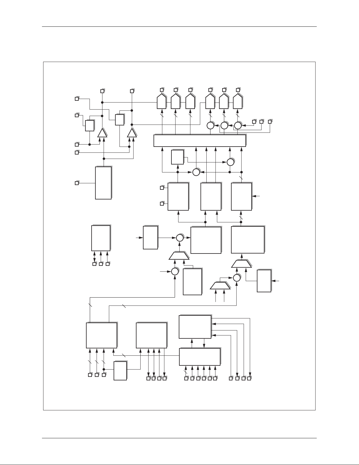
Figure 1-2. Detailed Block Diagram
COMP1
FB
FSADJ1
FSADJ2 VBIAS1 VBIAS2
VREF
Reference
Internal Voltage
FB
COMP2
Multiport YCrCb to NTSC/PAL /SECAM
DAC B
DAC A
DAC
10
Y
DAC
10
Luma
DAC C
DAC
10
CVBS
Delay
Out
Mux
U/V
DAC D
DAC
10
X
RGB
+
TTXREQTTXDAT
Color
Teletext
and CGMS
Space
Convert
DAC E
DAC
10
X
DLY
CVBS
+
10
DAC F
DAC
X
C
10
Modulator,
Mixer and
M_COMP_F
M_COMP_E
HUE_OFF
SECAM Filt.
M_COMP_D
Serial
Control
SIC
SID
10
Y
Alpha
8
2
8
OSD[7:0]
ALPHA[1:0]
Interface
ALTADDR
CRCB
Mixing
P[7:0]
10
8
656
Decoder
Sync
SYNC_AMP
Video
HSYNC*
Processor
M_Y
Timing
Control
FIELD
BLANK*
VSYNC*
9
+
X
Closed
8
VID[7:0]
Luminance
2x Upsample
Captioning,
Macrovision
Clock
PLL and
Generation
and
FIFO
Locking
VIDCLK
VIDVALID
and
Cross Color
M_CR
Control
VIDVACT
VIDHACT
Peaking Filt.
M_CB
VIDFIELD
and 2X
1.3 MHz LPF
X
XTI
CLKO
CLKIN
Matrix
Upsample/
Multiplication
Burst
XTO
Processor
BST_AMP
861_028
1-6 Conexant D860DSA
Page 17

2
2.0 Inputs and Timing
2.1 Reset
The Bt860/Bt861 has the following reset methods:
• power-up reset
• RESET* pin reset
• software reset register bit
Power-up reset occurs when the part is powered-up. A pin reset occurs when
the RESET* pin is held low. (It is recommended that the pin be held low for a
minimum of 50 system clock cycles.) Both power-up and pin reset cause the
initialization of all chip functions, including video timing and serial programming
registers.
Writing a 1 to register bit SRESET (1B[7]) resets all serial programing
registers to their default states, listed in Section 5.0.
2.1.1 Initialization and Power-up Configuration
At power-up all registers reset to their initial values (see Section 5.0).
The state of the FIELD pin at power-up (or pin reset) determines the default
state of the PCLK_SEL register bit and the initial clock source. If the FIELD pin
is pulled high, the initial clock source is the CLKIN pin; if the FIELD pin is
pulled low, the initial clock source is from the PLL and requires a crystal at the
XTI and XTO pins. If not loaded, the FIELD pin is pulled low with the pin’s
internal pull-down resistor.
The power-up configuration is interlaced NTSC-M, 27 MHz black burst
video, as listed in the default values of the register bit map.
To enable active video, black burst video must be turned off by setting
NOTE:
register bit EACTIVE (1D[1]) to 1. Other video configurations must be
programmed using the part’s serial programming interface registers.
D860DSA Conexant 2-1
Page 18
2.0 Inputs and Timing Bt860/861
2.2 Digital Video Ports
Multiport YCrCb to NTSC/PAL /SECAM
2.2 Digital Video Ports
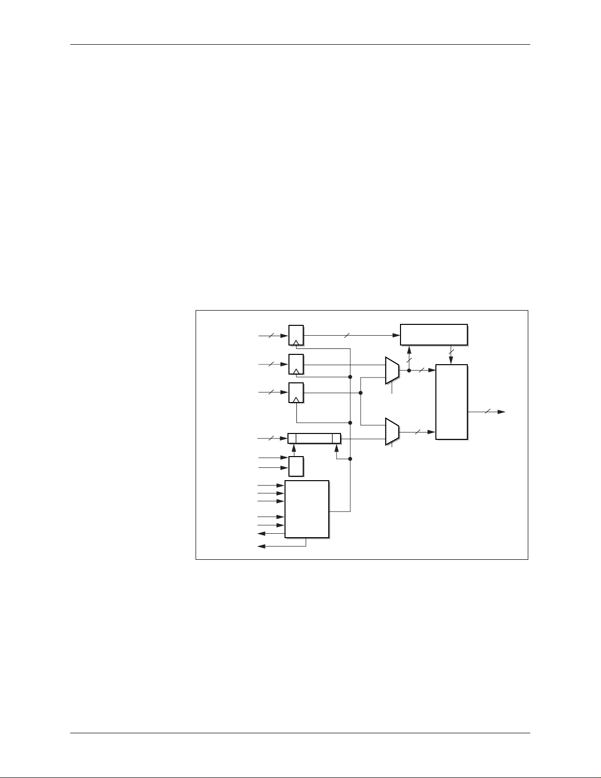
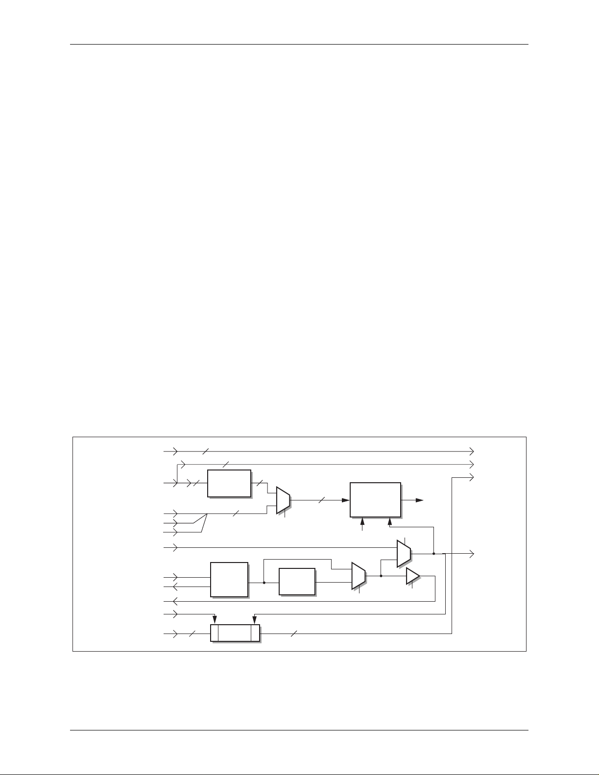
Internally, data to the Bt860/861 is treated as either video, overlay, or alpha data.
Video data is the primary visual program content, while overlay data is used for
informational or navigational content displayed over the visual program. Alpha
data controls the pixel blending of the video and overlay content. Sufficient
flexibility exists in the Bt860/861 to allow for a variety of source and blending
configurations and interesting visual effects.
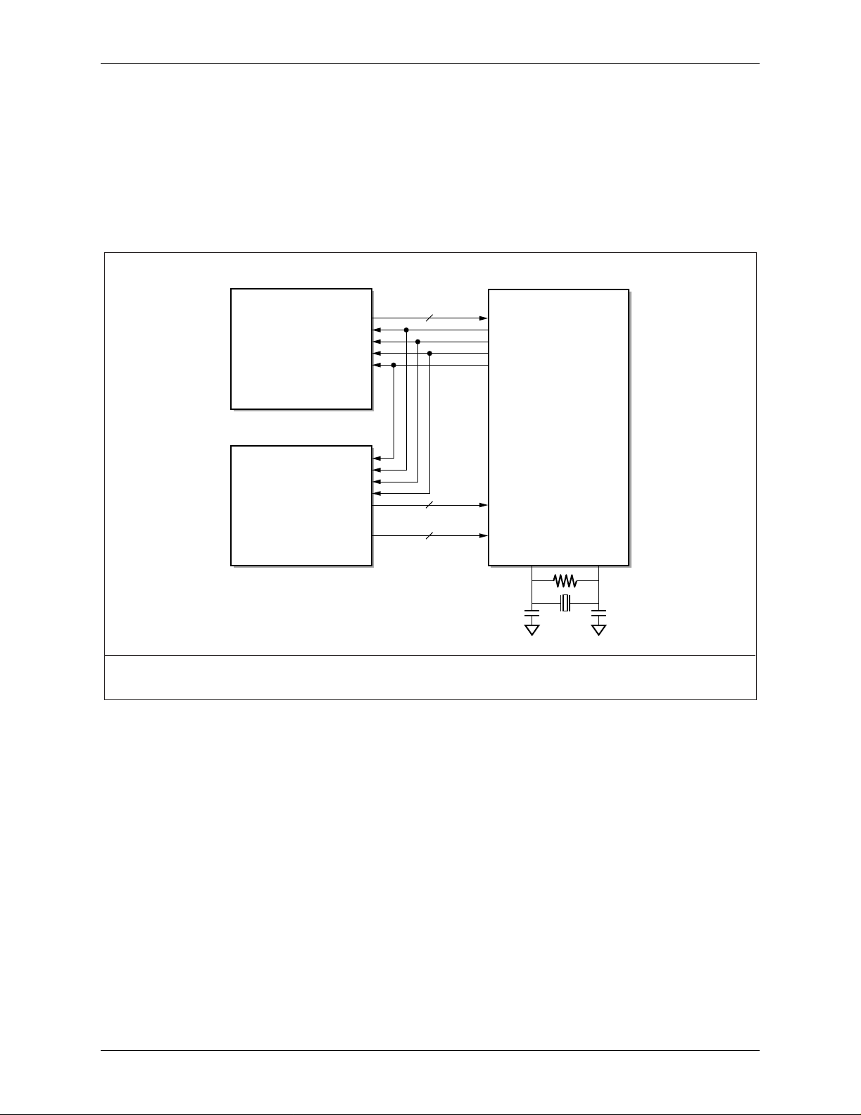
Video data is supplied by either the P (Primary Video) port, or the VID
(Secondary Video) port. Overlay data can be supplied by either the P port or the
OSD (On Screen Display) port. Alpha data can be supplied by the ALPHA port,
or embedded in the two LSBs of the overlay luminance data. Figure 2-1
illustrates the pixel latching and blending mechanism.
Figure 2-1. Pixel Latching and Blending Mechanism
ALPHA
OSD
2
8
8
P
2
OVERLAY_SEL
2
Overlay
Stream
Blend
Detection
8
4
Pixel
Blender
8
VID
VIDCLK
VIDVALID
VIDHACT
VIDVACT
VIDFIELD
CLKIN
XTI
XTO
CLKO
8
VIDEO_SEL
PLL
and
Clock
Logic
8
Video
Stream
861_042
2-2 Conexant D860DSA
Page 19

Bt860/861 2.0 Inputs and Timing
Multiport YCrCb to NTSC/PAL /SECAM
2.2.1 The P Port
The P port can accept video data from a variety of digital video sources. It is
designed specifically to interface directly with commercial MPEG video decoders
and D1 digital video sources. The P port supports both ITU-R BT.601 timing
(HSYNC* and VSYNC* signals), and ITU-R BT.656 timing (SAV and EAV
codes).
Data on the P[7:0] pins can be treated as either video or overlay data,
controlled by the VIDEO_SEL (1A[3]) and OVRLAY_SEL (1A[4]) register bits
(see Figure 2-1). Data on this port must be presented in 8-bit YCrCb 4:2:2 digital
video format. The P[7:0] pins are latched using the system clock as configured
using register bits PCLK_SEL (19[7]) and PCLK_EDGE (19[1]).
2.2.2 The VID Port
The VID port is specially configured for broadcast video sources, such as from a
television tuner or local cable system. It can accept a 27 MHz YCrCb 4:2:2 video
stream at the same pixel rate as the other ports, or it can accommodate alternate
clock rates, such as the 8xF
decoders. Since the time base for these sources is external to the system and
therefore asynchronous to the local pixel clock, the Bt860/861 provides a
mechanism that synchronizes these two domains. When using the VID port in
locking mode, the Bt860/861 immediately synchronizes its vertical timing to the
vertical timing presented on the VIDVACT pin, and gradually adjusts its
horizontal timing and clock rate to further synchronize with the VID port.
VIDCLK latches the incoming data into a FIFO, and data is extracted at the
appropriate pixel rate for internal processing.
The average active horizontal pixel count must be equal to the value
programmed into the HACTIVE register field. For example, the Bt835 generates
pixels at a rate of 14.32 Mpix/s when used for NTSC video capture, but the actual
valid pixel count per line is determined by the video mode required. For support
of 27 MHz streams, 720 valid pixels will be delivered per line. This configuration
is compatible with other video devices connected to the Bt860/861 and running
with a continuous pixel rate of 13.5 Mpix/s. The Bt860/861 will generate the
necessary video timing and pixel clock to act as master for the other video device.
The VID port can be configured as the video source by setting register bit
VIDEO_SEL (1A[3]) to 1. Data on this port must be presented in 8-bit YCrCb
4:2:2 digital video format.
2.2 Digital Video Ports
clock rate used by the Bt835 family of video
sc
2.2.3 The OSD Port
The OSD port is functionally very similar to the P port, except that it cannot decode
ITU-R BT.656 timing. As the overlay source, this port can be mixed with the video
stream using one of the alpha-mixing modes described in Section 2.2.5. While
intended as an overlay source, the OSD port can be configured to be the sole image
content by using the appropriate blend programming.
The overlay source is selected by setting register bit OVRLAY_SEL (1A[4])
to 1. Data on this port must be presented in 8-bit YCrCb 4:2:2 digital video
format. The OSD[7:0] pins are latched using the system clock as configured by
register bits PCLK_SEL (19[7]) and PCLK_EDGE (19[1]).
D860DSA Conexant 2-3
Page 20

2.0 Inputs and Timing Bt860/861
2.2 Digital Video Ports
Multiport YCrCb to NTSC/PAL /SECAM
2.2.4 Overlay Modes and Alpha Blending
The Bt860/861 can be configured to display only a single video stream, or to mix
any combination of two data ports (P, VID, and OSD). Programming register field
ALPHAMODE (1A[6:5]) to 00 and register bit BLENDMODE (1A[7]) to 1
selects the internal video bus as the sole source of data, regardless of the alpha
source. In this mode, either the VID port or the P port can be used as the video
source, which is selected by register bit VIDEO_SEL (1A[3]). Other
combinations of the ALPHAMODE and BLENDMODE programming will allow
blending of the video and overlay buses. Table 2-1 lists all valid input modes.
Table 2-1. Alpha Blending Configurations
Configuration Programming
Use
Video source
VID None None None 100 1 X No
VID P ALPHA[1:0] 1 bit
VID P ALPHA[1:0] 2 bit
VID P ALPHA[1:0] 4 bit
VID P P LSBs 2 bit
VID OSD ALPHA[1:0] 1 bit
VID OSD ALPHA[1:0] 2 bit
VID OSD ALPHA[1:0] 4 bit
VID OSD OSD LSBs 2 bit
P None None None
P OSD ALPHA[1:0] 1 bit
P OSD ALPHA[1:0] 2 bit
P OSD ALPHA[1:0] 4 bit
P OSD OSD LSBs 2 bit
NOTE(S):
Overlay source
X or XX = Don’t care.
Alpha Source
Blending depth
BLENDMODE
101 1 0 Yes
110 1 0 Yes
111 1 0 No
0XX 1 0 Yes
101 1 1 Yes
110 1 1 Yes
111 1 1 No
0XX 1 1 Yes
100 0 X No
101 0 1 Yes
110 0 1 Yes
111 0 1 No
0XX 0 1 Yes
ALPHAMODE
VIDEO_SEL
OVERLAY_SEL
ALPHA_LUT_X
Data from the overlay source may be applied with varying levels of
transparency, from fully transparent, no overlay, to fully opaque, full overlay. A
4-bit blend multiplier provides sixteen levels of mixing. The value 1111 is a
special case allowing the overlay data to pass completely unmixed. In all other
cases the value applied to the video path is (1 – blend / 16), and the value applied
to the overlay path is (blend / 16), where blend is the 4-bit multiplier value.
Two methods are used to generate the 4-bit multiplier. The multiplier value
can come either from a four-entry by 4-bit lookup table (LUT), or directly from
the ALPHA pins. In both cases, the blend multiplier value will be applied to both
luma and chroma for the co-sited components (Cb0:Y0:Cr0) and a separate
multiplier applied for the (Y1) component.
2-4 Conexant D860DSA
Page 21
Bt860/861 2.0 Inputs and Timing
Multiport YCrCb to NTSC/PAL /SECAM
2.2.5 Alpha Pin Blending
The ALPHA[1:0] pins are used to select the amount of blending per pixel when
BLENDMODE = 1. The pins are sampled at the system clock rate and samples
during both luma and chroma components may be captured to create 1-, 2-, or
4-bit blend factors. For 1- and 2-bit blend modes, the multiplier LUT (in registers
ALPHA_LUT_0 through ALPHA_LUT_3 is programmed with user-defined
multiplier values.
In 1-bit blend mode, the ALPHA[0] pin indexes registers ALPHA_LUT_0
and ALPHA_LUT_3 to generate the multiplier value. In 2-bit blend mode, the
ALPHA[1:0] pins are used as a 2-bit index for registers ALPHA_LUT_0 through
ALPHA_LUT_3.
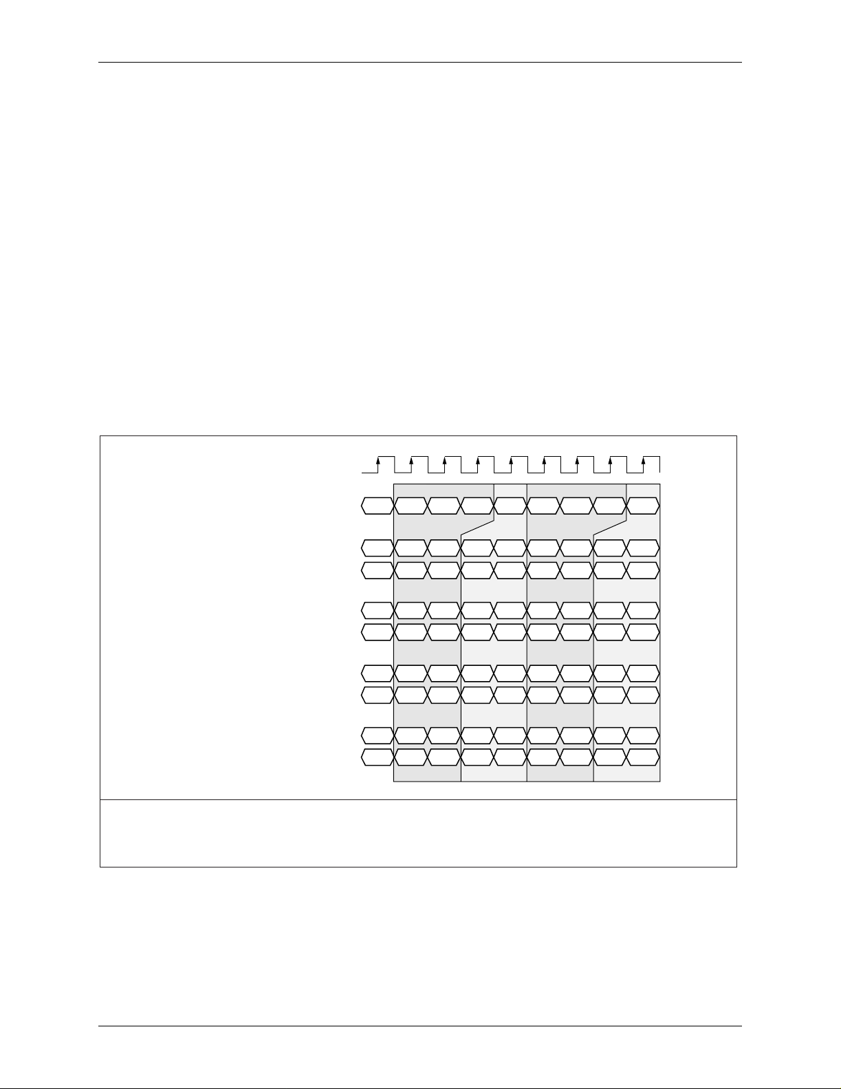
In 4-bit blend mode, the four bits required are captured in successive load
clocks from ALPHA[1:0]. The two LSBs of the 4-bit value are latched during the
luma portion of the overlay data load, and the two MSBs are latched during the
chroma component load. These four bits provide a direct multiplier for the
blending module. Figure 2-2 illustrates the alpha blending timing diagram.
Figure 2-2. Alpha Blending Timing Diagram
System Clock
2.2 Digital Video Ports
8-bit Overlay
Data
4-bit Alpha
2-bit Alpha
OSD[7:0]/P[7:0]
ALPHA[1]
ALPHA[0]
ALPHA[1]
ALPHA[0]
Cb0Y0Cr0Y1Cb2Y2Cr2Y
A[3]0A[1]0A[3]1A[1]1A[3]2A[1]2A[3]3A[1]
A[2]0A[0]0A[2]1A[0]1A[2]2A[0]2A[2]3A[0]
A[1]
A[0]
0
0
A[1]
A[0]
1
1
ALPHA[1]
NOTE(S):
1-bit Alpha
2-bit Content-
based Alpha
ALPHA[0]
OSD[1]/P[1]
OSD[0]/P[0]
A[0]
A[1]
A[0]
0
0
0
A[0]
A[1]
A[0]
1
1
1
1. Shaded areas indicate which video components are affected by each multiplier or index.
2. A blank data packet means this data carries no alpha information.
A[1]
A[0]
A[0]
A[1]
A[0]
3
3
3
2
2
2
2
2
A[1]
A[0]
A[0]
A[1]
A[0]
3
3
3
3
3
861_026
2.2.6 Content-based Blending
Content-based blending uses the two LSBs of the overlay byte associated with the luma
pixel to address the multiplier lookup table (registers ALPHA_LUT_0 through
ALPHA_LUT_3). This method is selected by setting BLENDMODE = 0, and is a
convenient means of using blending when no alpha pins exist from the overlay device.
D860DSA Conexant 2-5
Page 22

2.0 Inputs and Timing Bt860/861
2.3 Configurations and Timing
Multiport YCrCb to NTSC/PAL /SECAM
2.3 Configurations and Timing
The Bt860/861 is capable of various ITU-R BT.601, ITU-R BT.656, and
decoder-locked configurations. Table 2-2 lists several ITU-R BT.601 and
ITU-R BT.656 configurations, and Section 2.3.3 discusses decoder-locked
configurations. In any of these configurations, it is possible to synchronize a
primary video source with an alternate video source. These two sources can then
be alpha-mixed, or independently selected for external display. Alpha mixing is
discussed in detail in Section 2.2.5.
Table 2-2. Configurable Timing States
Description
Bt860/861 is timing master,
HSYNC*, VSYNC*, and FIELD
are outputs.
(1)
Timing
Mode
,
100 1
SLAVE EN_656 SYNC_CFG
Bt860/861 is timing slave, timing
derived from HSYNC*, VSYNC*,
and BLANK* signals
Bt860/861 is timing slave, timing
derived from ITU-R BT .656 codes.
HSYNC*, and VSYNC* are
unused.
Bt860/861 is timing slave, timing
derived from ITU-R BT .656 codes.
HSYNC*, VSYNC*, and FIELD
are outputs.
NOTE(S):
(1)
Decoder locking using the VID port requires the part to be in timing mode 1, except
SYNC_CFG = 1 is only required if synchronization with other sources is required.
(2)
Either the BLANK* pin or the HBLANK, VBLANK, HACTIVE, and VACTIVE register can be
used for blanking.
3. Configurations not listed are not recommended.
4. X = Don’t care.
(2)
.
(1)
210 X
311 0
411 1
2-6 Conexant D860DSA
Page 23
Bt860/861 2.0 Inputs and Timing
Multiport YCrCb to NTSC/PAL /SECAM
2.3.1 ITU-R BT.601 Configurations and Timing
Master and slave ITU-R BT.601 configurations are listed in Table 2-2 as timing
modes 1 and 2. Timing mode 1 is the ITU-R BT.601 master mode. An example
connection diagram is illustrated in Figure 2-3. In this example, both video
sources are slaved to the Bt860/861.
.
Figure 2-3. Timing Mode 1 Connection Example
Video Slave Bt860/861
8
Optional OSD Source, Timing Slave
P[7:0]
HSYNC*
VSYNC*
CLKO
FIELD
2.3 Configurations and Timing
(1)
NOTE(S):
(1)
It is not required that the clock be sourced from the Bt860/861.
8
2
OSD[7:0]
ALPHA[1:0]
XTI XTO
861_009
D860DSA Conexant 2-7
Page 24
2.0 Inputs and Timing Bt860/861
2.3 Configurations and Timing
Timing mode 2 is the ITU-R BT.601 slave mode. An example connection
diagram is illustrated in Figure 2-4. In this example, the source feeding the P port
is the timing master, and both the optional OSD source and the Bt860/861 are
timing slaves. Although additional sources are shown in these diagrams, it is not
necessary to have more than one video source.
Figure 2-4. Timing Mode 2 Connection Example
Video Master Bt860/861
Optional OSD Source, Timing Slave
Multiport YCrCb to NTSC/PAL /SECAM
8
8
P[7:0]
HSYNC*
VSYNC*
(1)
CLKIN
BLANK*
OSD[7:0]
NOTE(S):
(1)
It is not required that the clock is sourced external to the Bt860/861.
When the Bt860/861 is configured for ITU-R BT.601 timing, the HSYNC*,
VSYNC*, FIELD, and BLANK* pins synchronize the Bt860/861 to external
video sources. In master mode, HSYNC* field, and VSYNC* are outputs and the
BLANK* pin is not used. All timing is generated internally and blanking is
determined by the HBLANK, VBLANK, HACTIVE, and VACTIVE registers. In
slave mode, HSYNC*, VSYNC* and BLANK* are inputs and the encoder’s
timing is controlled by an external master. Blanking is set either by the internal
HBLANK, VBLANK, HACTIVE, and VACTIVE registers (register bit
BLK_IGNORE = 1) or by a blanking signal on the BLANK* pin (register bit
BLK_IGNORE = 0).
2
ALPHA[1:0]
861_007
2-8 Conexant D860DSA
Page 25
Bt860/861 2.0 Inputs and Timing
Multiport YCrCb to NTSC/PAL /SECAM
If the registers are used to determine video blanking (register bit
BLK_IGNORE = 1), the first component of the first active pixel of a line should
be presented to the encoder at HBLANK + 2 rising system clock edges after the
falling edge of HSYNC* for master mode, and HBLANK + 3 rising system clock
edges after the falling edge of HSYNC* for slave mode. The correct order of the
pixel components is Cb
timing relationship.
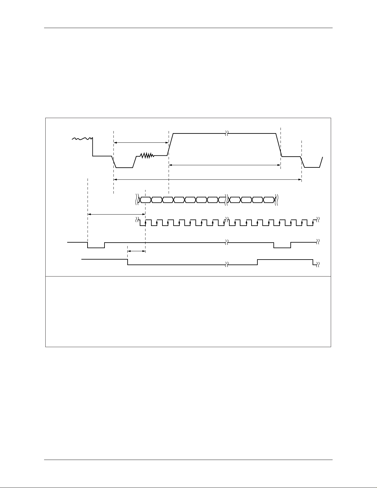
Figure 2-5. Pixel Timing for Timing Modes 1 and 2
(1)
t
1
Video Out
Pixel
Data
System
Clock
(4)
t
4
Cb
Y
0
0
2.3 Configurations and Timing
, Y0, Cr0, Y1, Cb2, Y2, Cr2.... Figure 2-5 illustrates this
0
(2)
t
2
(3)
t
3
Cr
Cb
Y
0
1
Cr
Y
2
2
2
Pixel Timing
(5)
HSYNC*
t
5
BLANK*
NOTE(S):
(1)
Blanking times (t1) are listed in Tables 3-1 through 3-4. Desired front porch blanking is set by the HBLANK register.
HBLANK = t1 + 14
(2)
The number of active pixels per line (t2) is set by the HACTIVE register.
(3)
The total number of system clocks per line (t3) is set by the HCLK register.
(4)
The first component of the first active pixel of the line should be placed HBLANK + 2 (or 3 for slave mode) rising system
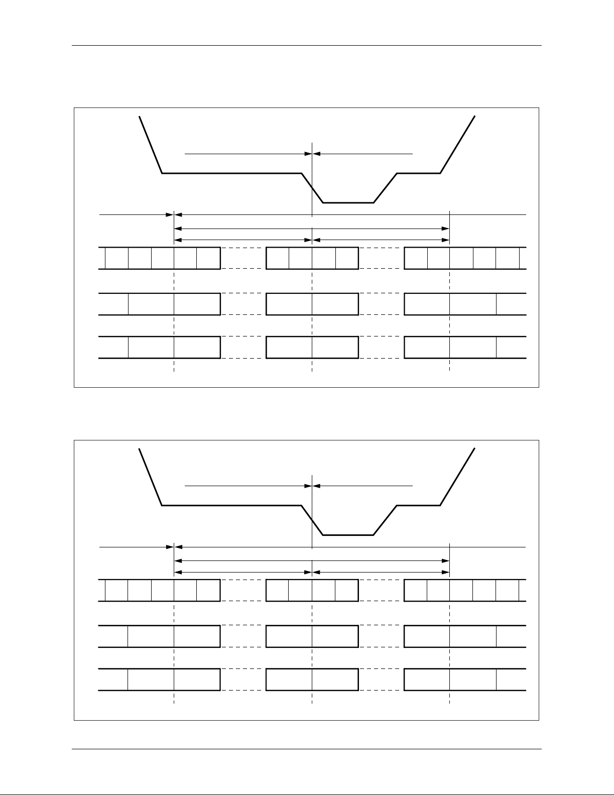
clock edges after falling HSYNC*(t
(5)
When the BLANK* pin is used, the first component of the first pixel must arrive 3 rising system clock edges after the
falling edge of BLANK* (t
).
5
) in order to coincide with the end of horizontal blanking.
4
If the BLANK* signal is used to determine video blanking (in slave mode
only), the first component of the first active pixel of a line should be presented to
the encoder three rising system clock edges after the falling edge of the BLANK*
signal. Figure 2-5 illustrates this relationship.
861_006
D860DSA Conexant 2-9
Page 26
2.0 Inputs and Timing Bt860/861
2.3 Configurations and Timing
The HBLANK register sets the line blanking time from the midpoint of the
falling edge of the analog horizontal sync pulse to the end of blanking. The
HACTIVE register sets the number of active pixels after the horizontal blanking
period has ended. See Tables 3-1 through 3-4 for appropriate HBLANK and
HACTIVE programming values for various NTSC, PAL, and SECAM video
standards.
Pixel and data timing (P, OSD, ALPHA, HSYNC*, VSYNC*, BLANK*) are
by default, latched into the Bt860/861 on the rising edge of the system clock, but
can be latched on the falling edge of the system clock if register bit PCLK_EDGE
(19[1]) is set high. The system clock can be seen on CLKO or CLKIN when
appropriate. Legal setup and hold times must be observed.
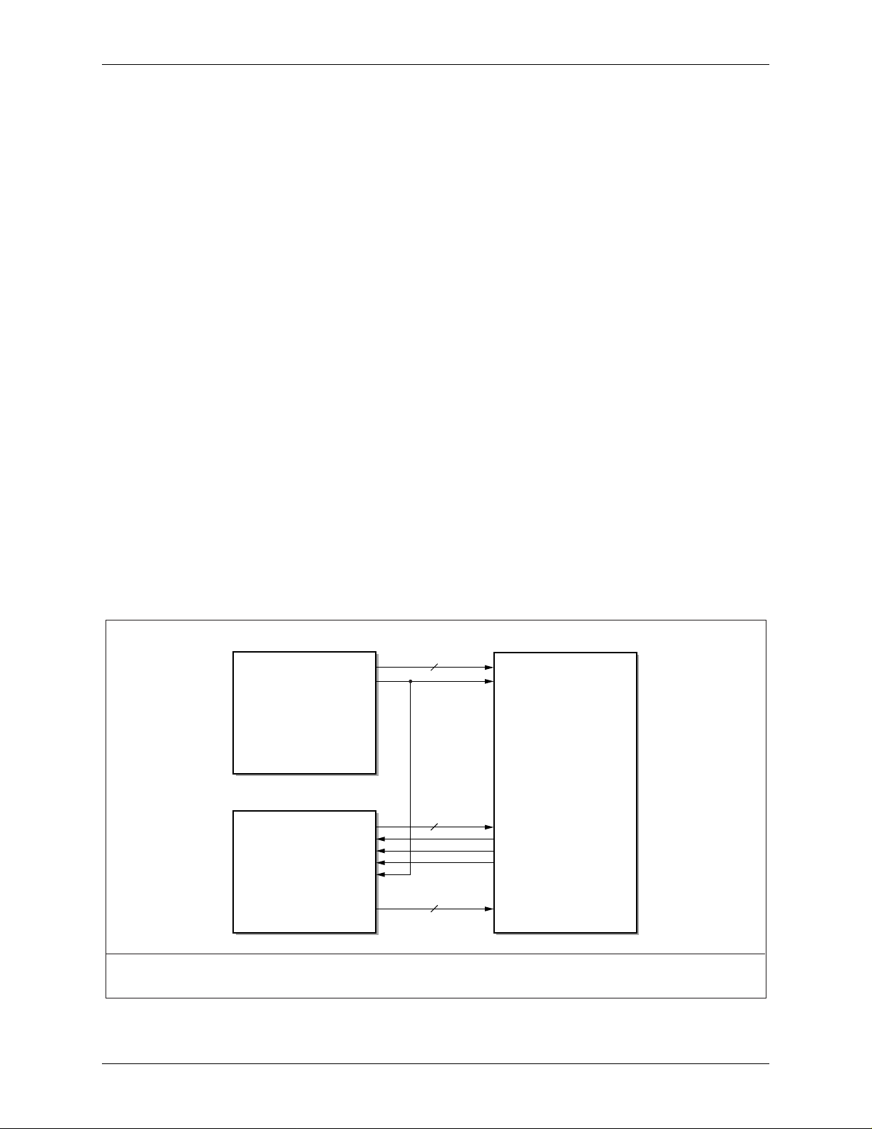
2.3.2 ITU-R BT.656 Timing
Data on the P port can be routed through the part’s ITU-R BT.656 timing
translator only when the system clock is 27 MHz, by setting register bit
EN_656 (1A[2]) high. This is accomplished using timing modes 3 or 4 (see
Table 2-2). Figure 2-6 illustrates an example connection diagram. ITU-R BT.656
timing derives vertical and horizontal timing information from the video data
stream (SAV and EAV codes). These codes are internally converted to HSYNC*
and VSYNC* signals, which can be then be produced on the Bt860/861’s
HSYNC*, VSYNC*, and FIELD pins. ITU-R BT.656 timing (also known as D1
timing) is illustrated in Figures 2-7 and 2-8. The resultant video is automatically
aligned to conform to ITU-R BT.656 video and blanking placement. The contents
of the HBLANK, HACTIVE, VACTIVE, and VBLANK registers are ignored,
except when register bit BLK_IGNORE = 1.
Multiport YCrCb to NTSC/PAL /SECAM
Figure 2-6. Timing Mode 3 and 4 Connection Example
CCIR656 Timing, Video Master Bt860/861
OSD Source, Timing Slave
NOTE(S):
(1)
It is not required that the clock is sourced external to the Bt860/861.
8
8
2
P[7:0]
(1)
CLKIN
OSD[7:0]
HSYNC*
VSYNC*
FIELD
ALPHA[1:0]
861_010
2-10 Conexant D860DSA
Page 27
Bt860/861 2.0 Inputs and Timing
Multiport YCrCb to NTSC/PAL /SECAM
Figure 2-7. 625 Line ITU-R BT.656 Timing
Analog Line n – 1
n
Digital Line
Luminance Samples
717 718
Cr Samples
Cb Samples
– 1 Digital Line
719 720 721 730 731 732 733 862 863 0 1 2
359 360 365 366 431 0 1
12
2.3 Configurations and Timing
O
H
Digital Blanking
T
Analog Line
132
n
n
T
359 360 365 366 431 0 1
T
: luminance sampling period
Figure 2-8. 525 Line ITU-R BT.656 Timing
Analog Line n – 1
n
Digital Line
Luminance Samples
717 718
Cr Samples
– 1 Digital Line
719 720 721 734 735 736 737 856 857 0 1 2
359 360 367 368 428 0 1
16
861_005a
O
H
Digital Blanking
T
Analog Line
122
n
n
T
Cb Samples
359 360 367 368 428 0 1
T
: luminance sampling period
861_005b
D860DSA Conexant 2-11
Page 28

2.0 Inputs and Timing Bt860/861
2.3 Configurations and Timing
In this configuration, the Bt860/861 is a slave to the ITU-R BT.656 data
stream. However, the HSYNC*, VSYNC* and FIELD pins can be configured as
outputs for synchronization with a video slave on the OSD port. While in this
configuration, the HSYNC*, VSYNC*, and FIELD timing is identical to
ITU-R BT.601 master mode timing.
2.3.3 VID Port (Video Decoder Locked) Timing
The VID port can accept video signals from a video decoder, such as the Bt835,
and is buffered using a FIFO to support asynchronous video streams. The internal
logic will automatically pulls data from the FIFO when required. The data lines
for the VID port are VID[7:0], and the control lines are VIDCLK, VIDHACT,
VIDVACT, VIDFIELD, and VIDVALID. Figure 2-9 illustrates an example
configuration using the Bt835 and the Bt860. The PLL and the horizontal and
vertical counters are adjusted to track the incoming data on the VID port. The
Bt860/861 can be configured to output HSYNC* and VSYNC* signals in order
to synchronize with the P, OSD, and ALPHA signals. Timing mode 1 must be
used when the VID port is selected in conjunction with a source on the P or OSD
ports. The PLL (using the XTI and XTO inputs) must be selected as the system
clock source.
Multiport YCrCb to NTSC/PAL /SECAM
2-12 Conexant D860DSA
Page 29
Bt860/861 2.0 Inputs and Timing
Multiport YCrCb to NTSC/PAL /SECAM
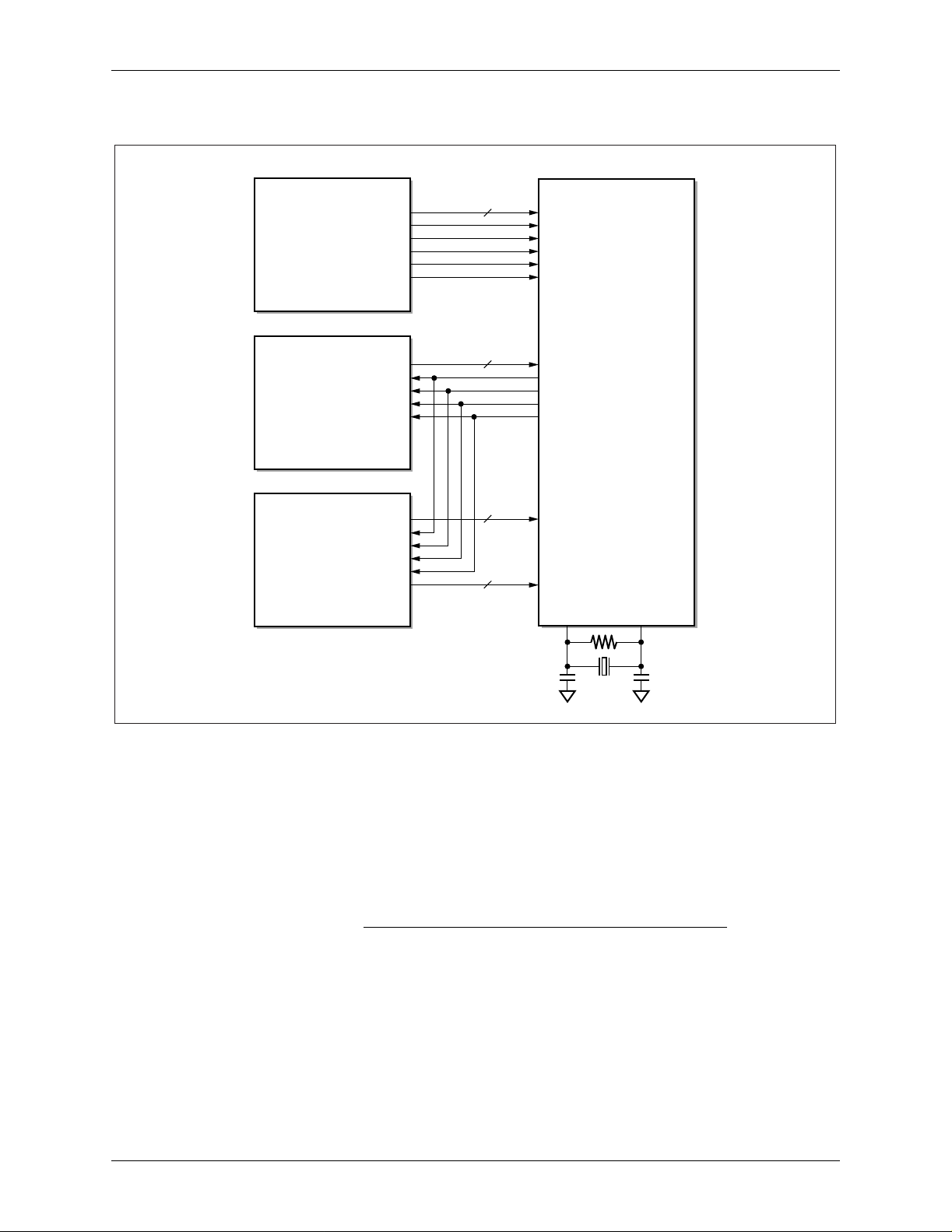
Figure 2-9. Video Decoder Connection Example
Bt835 Video Decoder Bt860/861
VD[15:8]
CLKX2
VALID
ACTIVE
VACTIVE
FIELD
MPEG-2 Decoder
Graphic Processor
2.3 Configurations and Timing
8
8
8
VID[7:0]
VIDCLK
VIDVALID
VIDHACT
VIDVACT
VIDFIELD
P[7:0]
CLKO
HSYNC*
VSYNC*
FIELD
OSD[7:0]
2
ALPHA[1:0]
XTI XTO
Follow these steps to lock a video decoder to this port:
Connect to the data and control pins as illustrated in Figure 2-9.
1.
Select the correct effective clock frequency using the PLL_FRACT and
2.
PLL_INT registers, and choose the XTAL inputs as the system clock
source using register bit PCLK_SEL (19[7]). See Section 2.4.1, and the
PLL_FRACT and PLL_INT register descriptions.
Set these locking registers to the following values:
3.
FIELD NAME VALUE
XL_MDSEL[1:0] 11
XL_SATEN 1
XL_SAT[3:0] 1
Set the part for Timing Mode 1 (see Table 2-2).
4.
Initiate locking by setting the LOCK (1C[5]) register bit high and the
5.
LC_RST (1C[6]) register bit low.
861_008
When unlocking the Bt861 to a source on the VID port, set the
NOTE:
LOCK (1C[5]) register bit low and the LC_RST (1C[6]) register bit high.
D860DSA Conexant 2-13
Page 30
2.0 Inputs and Timing Bt860/861
2.4 Clock Selection
2.4 Clock Selection
The internal pixel clock (PCLK) can be derived from either the CLKIN input or
the crystal inputs. The PCLK_SEL register bit (19[7]) controls which of these
two inputs will become the pixel clock.
2.4.1 Crystal Inputs and the PLL
The crystal inputs (XTI and XTO) drive a buffered oscillator to create a clock.
This clock is routed through the PLL if register bit BY_PLL (1D[3]) is 0, and
bypasses the PLL untouched if BY_PLL is 1. Figure 2-10 illustrates the clock
block diagram. If PCLK_SEL is low, this becomes the system clock.
The PLL_FRACT and the PLL_INT registers determine the PLL clock
frequency multiplier. The default setting generates a 27.0 MHz clock, using a
14.31818 MHz crystal.
If the VID port is enabled using the LOCK (1C[5]) register bit, the PLL is
controlled by the tracking servo mechanism.
The frequency programmed through PLL_FRACT and PLL_INT is used as a
base around which the VID port locking mechanism adjusts the system clock.
The PLL_FRACT and PLL_INT registers remain unaffected by the locking
mechanism, and when locking is disabled (through the LOCK bit), the
PLL_FRACT and PLL_INT registers once again determine the exact PLL
frequency.
Multiport YCrCb to NTSC/PAL /SECAM
Figure 2-10. Timing and Clock Block Diagram
OSD[7:0]
P[7:0]
HSYNC*
VSYNC*
BLANK*
CLKIN
XTI
XTO
CLKO
VIDCLK
VID[7:0]
8
8
CCIR656
8
Timing
Translator
3
Xtal
Inverter
and Buffer
88
FIFO
3
1
0
EN_656
PLL
OSD[7:0]
P[7:0]
VID[7:0]
3
Encoder
Timing
Block
SLAVE
1
0
BY_PLL
System
Block
PCLK_SEL
1
0
CLKO_DIS
System
Clock
861_025
2-14 Conexant D860DSA
Page 31

3.1.1 Video Standards
3
3.0 Digital Processing and Functionality
3.1 Video
The Bt860/861 supports worldwide video standards, including NTSC-M
(N. America, Taiwan, Japan), PAL-B, D, G, H, I (Europe, Asia), P AL-M (Brazil),
PAL-N (Uruguay, Paraguay), PAL-Nc (Argentina), PAL-60, NTSC-443, and
SECAM.
Table 3-1 lists the target video timing and amplitude used to generate the
appropriate register programming for various forms of NTSC, PAL, and SECAM
as listed in Tables 3-2, 3-3, and 3-4 respectively. These tables provide the
programming values of only those registers required to create that particular
video standard. Ancillary data, input configuration, and ignored or common value
register values are not shown. Video parameter registers which are not relevant to
a particular standard are described as such in the register detail section of this
document.
Table 3-2 lists the register values required to program the various forms of
PAL and NTSC in ITU-R BT.601 resolution, and Table 3-3 lists the register
values required to program the various forms of PAL and NTSC in square pixel
resolution. Table 3-4 lists register values required to program the encoder for
SECAM output, with and without synchronization bottleneck pulses.
D860DSA Conexant 3-1
Page 32

Bt860/861
N/A
for=4406250,
fob=4250000
2.51
(9 cycles)
PAL-N PAL-Nc SECAM
PAL-
B,D,G,H,I
200 200 200
(1)
200
2.25
(10 cycles)
2.25
(10 cycles)
Multiport YCrCb to NTSC/PAL /SECAM
(4)
(4)
23
309
(4)
(4)
23
309
(4)
(4)
23
309
(4)
(4)
23
309
Video Standard
150 150 150 150 150
2.25
(10 cycles)
2.52
(9 cycles)
2.25
(10 cycles)
2.514
(9 cycles)
2.514
(9 cycles)
3579545 3579545 4433618.75 3579611.49 4433618.75 4433618.75 4433618.75 3582056.25
(Hz)
(2)
(3)
(3)
22
262
(3)
(3)
22
262
(3)
(3)
22
262
(3)
(3)
22
262
(3)
(3)
22
262
9.2 [9.037] 9.2 9.2 9.2 9.2 10.5 [9.778] 9.2 10.5 10.5
(5)
Parameter Description NTSC-M NTSC-J NTSC-443 PAL-M PAL-60
HSYNC Width (µs) 4.7 4.7 4.7 4.7 4.7 4.7 4.7 4.7 4.7
HSYNC and VSYNC Height (V) 0.286 0.286 0.2857 0.2857 0.3 0.3 0.2857 0.3 0.3
HSYNC Rise/Fall Time
(10% to 90%) (ns)
Burst or Subcarrier Start (µs) 5.3 5.3 5.3 5.8 5.3 5.6 5.6 5.6 5.6
Burst Width (µs)
Subcarrier Frequency
Burst or Subcarrier Height (V) 0.2857 0.2857 0.2857 0.306 0.3 0.3 0.3 0.3 0.161
Phase Alternation NO NO NO YES YES YES YES YES NO
Number of Lines per Frame 525 525 525 525 525 625 625 625 625
Line Frequency (Hz) 15734.264 15734.264 15734.264 15734.264 15734.264 15625 15625 15625 15625
Field Frequency (Hz) 59.94 59.94 59.94 59.94 59.94 50 50 50 50
Setup YES NO YES YES NO NO YES NO NO
First Active Line
Last Active Line
3
Table 3-1. Target Video Parameters (1 of 2)
HSYNC to Blank End (µs)
3-2 Conexant D860DSA
Page 33

Bt860/861
Multiport YCrCb to NTSC/PAL /SECAM
PAL-N PAL-Nc SECAM
PAL-
B,D,G,H,I
.
clk
and F
sc
Video Standard
as given in ITU-R BT.470 instead of F
h
to F
sc
1.5[1.185] 1.5 1.5 1.5 1.5 1.5[0.889] 1.5 1.5 1.5
(5)
333332.532.52.5
Table 3-1. Target Video Parameters (2 of 2)
Parameter Description NTSC-M NTSC-J NTSC-443 PAL-M PAL-60
Black to 100% White (V) 0.661 0.714 0.661 0.661 0.7 0.7 0.661 0.7 0.7
Number of Lines each for
Blank Begin to HSYNC (µs)
Vertical Serration, Equalization
Value for PAL-I is 250 ns.
When programming the subcarrier increment, use relationship of F
Using NTSC line numbering convention from ITU-R BT.470.
Using PAL line numbering convention from ITU-R BT.470.
ITU-R BT.601 blanking values given in square brackets []
NOTE(S):
(1)
(2)
(3)
(4)
(5)
D860DSA Conexant 3-3
Page 34

Bt860/861
Multiport YCrCb to NTSC/PAL /SECAM
PAL-N PAL-Nc
PAL-
B,D,G,H,I
Video Standard
3
Table 3-2. Register Programming Values for NTSC and PAL Video Standards (ITU-R BT.601) (1 of 2)
Register Name Register No. NTSC-M NTSC-J PAL-M NTSC-443 PAL-60
625LINE16[5] 00000111
Parameter
Description
Number of Lines
AHSYNC_WIDTH 08[7:0] 7F 7E 7F 7F 7F 7F 7F 7F
Width of Analog
Horizontal
BURST_AMP 1F[7:0] 7A 7B 5E 7A 5E 5D 5D 5D
Sync Pulse
Burst Amplitude
CROSSFILT1D[0] 11111111
FM 16[2] 00000000
Cross Color Filter
Off
Frequency
HACTIVE 07[1:0]/06[7:0] 2C9 2C9 2C9 2C9 2C9 2BF 2CF 2BF
Modulated
Number of Active
Pixels
Per Line
HBLANK 0C[1:0]/0B[7:0] 108 108 108 108 108 128 108 128
to
H
Number of System
Clocks from O
HBURST_BEG 09[7:0] 8C 8E 9A 8C 8F 95 95 95
Active Video
Beginning of Burst
HBURST_END 0A[7:0] 54 52 5C 54 52 51 51 58
HCLOCK 05[3:0]/04[7:0] 6B4 6B4 6B4 6B4 6B4 6C0 6C0 6C0
End of Burst
Number of System
Clocks Per Line
M_CB 21[7:0] 8D 9B 8D 8D 9B 9B 9B 9B
M_CR 20[7:0] C7 DA C7 C7 DA DA DA DA
Cb Multiplier
Cr Multiplier
M_Y 22[7:0] 9A A5 9A 9A 9A A2 A2 A2
Y Multiplier
3-4 Conexant D860DSA
Page 35

Bt860/861
Multiport YCrCb to NTSC/PAL /SECAM
PAL-N PAL-Nc
PAL-
B,D,G,H,I
) as line #1 (see Figures 3-1 and 3-2).
V
PAL-M NTSC-443 PAL-60
NTSC-
JAPAN
Video Standard
Register Name Register No. NTSC-M
21F07C1F 21F07C1F 21F0A527 2A098ACB 2A098ACB 2A098ACB 2A098ACB 21F69446
29[7:0]/28[7:0]
27[7:0]/26[7:0]
NI 16[1] 00000000
MSC_DR
PAL 16[3] 00101111
PHASE_OFF38[7:0] 0000000000000000
SC_RESET16[7] 00011000
SETUP 16[4] 1 0 1 1 0 0 1 0
SYNC_AMP1E[7:0] E4E4E4E4F0F0E4F0
VACTIVE 0F[0]/0E[7:0] 0F1 0F1 0F1 0F1 0F1 11F 11F 11F
VBLANK0D[7:0] 1313131313171717
VSYNC_DUR16[6] 00000101
V
Internal timing and the values programmed into the registers reference the analog VSYNC pulse (O
Parameter
Description
Interlace Off
Phase Alternation
Subcarrier Phase
Offset
Subcarrier Reset
SETUP
Sync Tip to Blank
Amplitude
Number of Active
Lines
Number of Blanked
Lines from O
Analog and Digital
Vertical Sync
Table 3-2. Register Programming Values for NTSC and PAL Video Standards (ITU-R BT.601) (2 of 2)
Subcarrier
Increment
Duration
NOTE(S):
D860DSA Conexant 3-5
Page 36

Bt860/861
Multiport YCrCb to NTSC/PAL /SECAM
PAL-N PAL-Nc
PAL-
B,D,G,H,I
Video Standard
PAL-M NTSC-443 PAL-60
NTSC-
JAPAN
NTSC-M
System Clock Frequency (MHz)
Table 3-3. Register Programming Values for NTSC and PAL Video Standards (Square Pixel) (1 of 2)
Register Name Register No. 24.5454 24.5454 24.5454 24.5454 24.5454 29.5 29.5 29.5
625LINE16[5] 00000111
Parameter
Description
Number of Lines
AHSYNC_WIDTH08[7:0] 74747474748A8A8A
BURST_AMP 1F[7:0] 7C 7C 5F 7A 5D 5D 5D 5D
Width of Analog
Horizontal
Sync Pulse
Burst Amplitude
CROSSFILT1D[0] 11111111
FM 16[2] 00000000
Cross Color Filter
Off
Frequency
HACTIVE 07[1:0]/06[7:0] 289 289 289 289 289 300 314 300
Modulated
Number of Active
Pixels
HBLANK 0C[1:0]/0B[7:0] 0F0 0F0 0F0 0F0 0F0 140 11C 140
to
H
Per Line
Active Video
Number of System
Clocks from O
HBURST_BEG 09[7:0] 80 80 8B 80 80 A4 A4 A4
HBURST_END 0A[7:0] 3D 3D 4A 3D 3D 65 65 6E
HCLOCK 05[3:0]/04[7:0] 618 618 618 618 618 760 760 760
Beginning of Burst
End of Burst
Number of System
Clocks Per Line
3-6 Conexant D860DSA
Page 37

Bt860/861
Multiport YCrCb to NTSC/PAL /SECAM
PAL-N PAL-Nc
PAL-
B,D,G,H,I
Video Standard
) as line #1 (see Figures 3-1 and 3-2).
V
PAL-M NTSC-443 PAL-60
NTSC-
JAPAN
Register Name Register No. NTSC-M
25555555 25555555 254BF631 2E3DB902 2E3DB902 26798C0C 26798C0C 1F15C01E
29[7:0]/28[7:0]/
27[7:0]/26[7:0]
NI 16[1] 00000000
PAL 16[3] 00101111
PHASE_OFF38[7:0] 0000000000000000
SC_RESET16[7] 00011000
SETUP16[4] 10110010
SYNC_AMP1E[7:0] E4E4E4E4F0F0E4F0
VACTIVE 0F[0]/0E[7:0] 0F1 0F1 0F1 0F1 0F1 11F 11F 11F
M_CB 21[7:0] 90 9C 90 90 99 99 99 99
M_CR 20[7:0] CB DC CB CB D8 D8 D8 D8
M_Y 22[7:0] 99 A6 99 99 A2 A2 A2 A2
MSC_DR
VBLANK0D[7:0] 1313131313171717
VSYNC_DUR16[6] 00000101
V
Internal timing and the values programmed into the registers reference the analog VSYNC pulse (O
Parameter
Description
Interlace Off
Phase Alternation
Subcarrier Phase
Offset
Subcarrier Reset
SETUP
Sync Tip to Blank
Amplitude
Number of Active
Lines
Number of Blanked
Lines from O
Analog and Digital
Vertical Sync
Table 3-3. Register Programming Values for NTSC and PAL Video Standards (Square Pixel) (2 of 2)
Cb Multiplier
Cr Multiplier
Y Multiplier
Subcarrier
Increment
Duration
NOTE(S):
D860DSA Conexant 3-7
Page 38

Bt860/861
3
Multiport YCrCb to NTSC/PAL /SECAM
Table 3-4. Register Programming Values for SECAM
System Clock Frequency
Parameter Description Register Name Register Number
(MHz)
27 29.5
Number of Lines 625 Line 16[5] 1 1
Width of Analog Horizontal Sync Pulse AHSYNC_WIDTH 08[7:0] 7F 8B
Cross Color Filtering Off CR0SSFILT ID[0] 0 0
Upper Db Limit DB_MAX 34[1:0]/33[7:0] 5A3 529
Lower Db Limit DB_MIN 36[1:0]/35[7:0] 49F 43B
Upper Dr Limit DR_MAX 30[1:0]/2F[7:0] 5A3 529
Lower Dr Limit DR_MIN 32[1:0]/31[7:0] 49F 43B
Bottleneck Pulses FIELD_ID 1B[6]
(1)
0
FM Modulation FM 16[2] 1 1
Number of Active Pixels per Line HACTIVE 07[1:0]/06[7:0] 2C0 300
Number of System Clocks from O
to
H
HBLANK 0C[1:0]/0B[7:0] 128 140
Active Video
Beginning of Subcarrier HBURST_BEG 09[7:0] 97 A5
Number of System Clocks Per Line HCLOCK 05[3:0]/04[7:0] 6C0 760
Cb Multiplier M_CB A2 94 9A
Cr Multiplier M_CR C5 B5 BB
Y Multiplier M_Y 22[7:0] A4 A4
Subcarrier Increment for Db MSC_DB 2D[7:0]/2C[7:0]
284BDA13 24E1A08B
2B[7:0]/2A[7:0]
Subcarrier Increment for Dr MSC_DR 29[7:0]/28[7:0]
29C71C72 263CBEEA
27[7:0]/26[7:0]
Interlace Off NI 16[1] 0 0
Phase Alternation PAL 16[3] 0 0
Programmable Subcarrier Mode PROG_SC 1A[1] 0 0
Subcarrier Amplitude SC_AMP 86 86 85
Subcarrier Phase Pattern SC_PATTERN 1A[0] 0 0
Setup SETUP 16[4] 0 0
Sync Tip to Blank Amplitude SYNC_AMP 1E[7:0] F0 F0
Number of Active Lines VACTIVE 0F[0]/0E[7:0] 11F 11F
Number of Blanked Lines from O
(2)
V
VBLANK 0D[7:0] 17 17
Analog and Digital Vertical Sync Duration VSYNC_DUR 16[6] 1 1
NOTE(S):
(1)
(2)
To enable synchronization bottleneck pulses, this bit must be 1.
Internal timing and the values programmed into the registers reference the analog VSYNC pulse (OV) as line #1 (see
Figures 3-1 and 3-2).
(1)
0
3-8 Conexant D860DSA
Page 39

Bt860/861 3.0 Digital Processing and Functionality
3
Multiport YCrCb to NTSC/PAL /SECAM
3.1 Video
3.1.2 Analog Horizontal Sync
3.1.3 Analog and Digital Vertical Sync
3.0 Digital Processing and Functionality
3.1.1
Figure 3-1. NTSC Vertical Timing
3.1 Video
The duration of the horizontal sync pulse is determined by register
HSYNC_WIDTH (12[7:0]). The beginning of the horizontal sync pulse
corresponds to the reset of the internal horizontal pixel counter. The sync rise and
fall times are automatically controlled. The horizontal and vertical sync
amplitude is programmable using register SYNC_AMP (IE[7:0]).
The duration of the analog and digital vertical sync is determined by register bit
VSYNC_DUR (16[6]). If VSYNC_DUR = 0, 3.0 lines are selected; if
VSYNC_DUR = 1, 2.5 lines are selected. Tables 3-2, 3-3, and 3-4 list the
appropriate VSYNC_DUR settings for all supported standards.
Figures 3-1 and 3-2 illustrate 3.0 and 2.5 lines respectively.
(1)
O
V
Odd Field
NOTE(S):
(1)
Internal timing considers this point the start of the field (vertical reset).
Even Field
861_032
D860DSA Conexant 3-9
Page 40

3.0 Digital Processing and Functionality Bt860/861
3.1 Video
Figure 3-2. PAL Vertical Timing
(1)
O
V
NOTE(S):
(1)
Internal timing considers this point the start of the field (vertical reset).
Multiport YCrCb to NTSC/PAL /SECAM
Odd Field
Even Field
861_033
3.1.4 Analog Video Blanking
In master mode, and when register bit BLK_IGNORE = 1 in slave mode, register
fields HBLANK, VBLANK, HACTIVE, and VACTIVE control analog video
blanking. Together they define the active region, where pixels will be displayed.
VBLANK defines the number of lines from the leading edge of the analog
vertical sync (O
defines the number of active lines. HBLANK defines the number of system
clocks (minus 14) from the leading edge of horizontal sync to the first active
pixel. HACTIVE defines the number of active pixels per line.
In the slave mode, when BLK_IGNORE = 0, the BLANK* pin determines
analog blanking. The video from the start of horizontal sync through the end of
the burst, as well as the vertical lines with serration and equalization pulses is
automatically blanked.
) to the first active line (see Figures 3-1 and 3-2). VACTIVE
v
3-10 Conexant D860DSA
Page 41

Bt860/861 3.0 Digital Processing and Functionality
Multiport YCrCb to NTSC/PAL /SECAM
3.1.5 Subcarrier and Burst Generation
The Bt860/861 uses a 32-bit subcarrier increment to synthesize the subcarrier.
The value of the subcarrier increment required to generate the desired subcarrier
frequency for NTSC and PAL formats is found by:
M_SC_DR[31:0] = int (2
where f
frequency.
When available, use the relationship between HCLK and the subcarrier frequency
as given in ITU-R BT.470. For example:
NTSC-M: M_SC_DR[31:0] = int {[455 / (2 × HCLK)] × 2
PAL-B: M_SC_DR[31:0] = int {[(1135 / 4 + 1 / 625) / HCLK] × 2
Tables 3-2 and 3-3 lists the programming values for common NTSC and P AL
standards.
For SECAM formats, the two subcarrier frequency increments are defined by:
SECAM Dr: M_SC_DR[31:0] = int [(f
SECAM Db: M_SC_DB[31:0] = int [(f
Table 3-4 lists standard programming values for SECAM.
The HBURST_BEG register determines the start of burst (or subcarrier for
SECAM). In PAL and NTSC video formats the HBURST_END register
determines the end of the burst. The BURST_AMP register controls burst
amplitude. The burst is automatically blanked during the horizontal sync to
prevent generation of invalid sync pulses. Burst blanking is automatically
controlled and depends on which video format is selected. Burst rise and fall
times are internally controlled.
The SC_AMP register controls the SECAM subcarrier amplitude. In addition,
generation of the “bottleneck signals” for subcarrier line synchronization may be
enabled using the FIELD_ID register bit. Registers PROG_SC and
SC_PATTERN allow control of active line placement and subcarrier phase
sequencing.
is the encoder system clock rate and fsc is the desired subcarrier
clk
32
× fsc / f
clk
+ 0.5)
/ f
sc
/ f
sc
) × 232 + 0.5]
clk
) × 232 + 0.5]
clk
32
+ 0.5}
3.1 Video
32
+ 0.5}
D860DSA Conexant 3-11
Page 42

3.0 Digital Processing and Functionality Bt860/861
3.1 Video
3.1.6 Subcarrier Phasing (SC_H Phase)
For PAL and NTSC video formats, the subcarrier phase is set to 0 on the leading
edge of the analog vertical sync every four (NTSC) or eight (PAL) fields, unless
the SC_RESET bit is set to a logical 1. This is true for both interlaced and
non-interlaced outputs. In addition, the subcarrier phase can be adjusted by the
PHASE_OFF register. Each LSB change of PHASE_OFF corresponds to a
360 / 256 degree change in the phase.
Setting SC_RESET to 1 is useful when the subcarrier phase at the end of a
color field sequence is significantly different from 0.
3.1.7 Noninterlaced Operation
When programmed for noninterlaced master mode, the Bt860/861 always
displays the odd field. The FIELD signal stays low to indicate that the field is
always odd. A 30 Hz offset should be subtracted from the color subcarrier
frequency while in NTSC mode so the color subcarrier phase will be inverted
from field to field. Transition from interlaced to noninterlaced in master mode
occurs during odd fields to prevent synchronization disturbance.
Consumer VCRs can record noninterlaced video with minor noise
NOTE:
artifacts, but special effects (e.g., scan >2x) may not function properly.
Multiport YCrCb to NTSC/PAL /SECAM
3-12 Conexant D860DSA
Page 43

Bt860/861 3.0 Digital Processing and Functionality
Multiport YCrCb to NTSC/PAL /SECAM
3.2 Effects
3.2.1 Chrominance Disable
Setting register bit DCHROMA (17[2]) to 1 turns off the chrominance subcarrier
and colorburst.
3.2.2 Internal Filtering
Once the input data is converted to internal YUV format, the Y and UV
components are filtered and upsampled to the system clock frequency.
The luminance signal is always low-pass filtered using the upsampling filter
response illustrated in Figure 3-3. Additional peaking or reduction filters can be
enabled (see Figures 3-4 and 3-5), using the PKFIL_SEL register field and the
FIL_SEL register bit. When register bit FIL_SEL is set to 0, register field
PKFIL_SEL selects the peaking filters illustrated in Figure 3-7. When register bit
FIL_SEL is set to 1, register field PKFIL_SEL selects the reduction filters
illustrated in Figure 3-6. The peaking filters are optimized for high bandwidth
frequency response, and the reduction filters are optimized for step response
performance.
The default chrominance filter response is illustrated in Figure 3-8, but an
alternate wide bandwidth response can be selected using register bit
CHROMA_BW, as illustrated in Figure 3-9.
SECAM pre-emphasis filter responses are illustrated in Figures 3-10 and 3-11.
.
3.2 Effects
Figure 3-3. Luminance Upsampling Filter Figure3-4. Luminance Upsampling Filter with Peaking
and Reduction Options
0
–10
–20
–30
–40
Amplitude in dB
–50
–60
–70
–80
0 2 4 6 8 10 12
Frequency in MHz
861_015
0
–10
–20
–30
Amplitude in dB
–40
–50
–60
02468 10 12
Frequency in MHz
861_016
D860DSA Conexant 3-13
Page 44

3.0 Digital Processing and Functionality Bt860/861
3.2 Effects
Figure 3-5. Close-Up of Luminance Upsampling Filter
Figure 3-6. Luminance Reduction Filters Options
Multiport YCrCb to NTSC/PAL /SECAM
with Peaking and Reduction Options
2
0
–5
–10
Amplitude in dB
–15
–20
0 1 2 3 4 5 6 7 8
Frequency in MHz
861_017
0
–2
–4
Amplitude in dB
–6
–8
–10
0 1 2 3 4 5 6
Frequency in MHz
Figure 3-7. Luminance Peaking Filter Options Figure 3-8. Chrominance Filter
4
3.5
3
2.5
2
1.5
Amplitude in dB
1
0.5
0
0 1 2 3 4 5 6
Frequency in MHz
861_019
0
–10
–20
–30
–40
Amplitude in dB
–50
–60
0 0.5 1 1.5 2 2.5 3 3.5 4
Frequency in MHz
861_018
861_022
Figure 3-9. Chrominance Wide Bandwidth Filter Figure3-10. SECAM High Frequency Pre-emphasis
Filter
0
–10
–20
–30
Amplitude in dB
–40
–50
–60
0 1 2 3 4 5 6
Frequency in MHz
861_023a
6
4
2
0
8
6
Amplitude in dB
4
2
0
3.5 4 4.5 5
Frequency in MHz
861_021
3-14 Conexant D860DSA
Page 45

Bt860/861 3.0 Digital Processing and Functionality
Multiport YCrCb to NTSC/PAL /SECAM
Figure 3-11. SECAM Low Frequency Pre-emphasis
Filter
10
8
6
4
Amplitude in dB
2
0
0 0.1 0.2 0.3 0.4 0.5 0.6 0.7 0.8 0.9 1
Frequency in MHz
861_023
3.2.3 Internal Colorbars, Blue Field, and Black Burst
The Bt860/861 can be configured to generate 100% amplitude, 75% saturation
(100/7.5/75/7.5 for NTSC/PAL-M with set-up, 100/0/75/0 for PAL/SECAM)
colorbars by setting register bit ECBAR (17[1]) bit to a 1. The Bt860/861 can also
produce a blue field by setting register bit BLUE_FLD (17[6]) to 1, and black
burst by setting register bit EACTIVE (1D[1]) to 0. Pixel inputs are ignored while
any of these waveforms are being produced.
Example colorbars for different output formats are illustrated in Figures 3-12,
3-13, and 3-14. Specific levels are listed in Tables 3-5 through 3-8.
3.2 Effects
D860DSA Conexant 3-15
Page 46

3.0 Digital Processing and Functionality Bt860/861
3.2 Effects
Figure 3-12. YUV Video Format (Internal Colorbars)
White
A
wht
A
sync
y
A
wht
V(Pb)
Multiport YCrCb to NTSC/PAL /SECAM
Yellow
A
yel
A
yel
Cyan
A
cyn
A
cyn
Green
A
grn
A
grn
A
mgt
A
Magenta
mgt
Red
A
red
A
red
Blue
A
blu
A
blu
Black
A
blk
A
blk
A
A
wht
yel
U(Pr)
A
cyn
NOTE(S):
All “Ax“ values are relative to black, except for A
blk
and A
, which are relative to blank.
sync
Table 3-5. 100/0/75/0 Colorbars as Described in EIA-770.1. EIA-770.1
(1)
A
sync
Y (volts)
0.286 0.714 0.465 0.368 0.309 0.217 0.157 0.060 0
–
Pr (volts) 0 0 0.043
Pb (volts) 0 0
NOTE(S):
(1)
EIA-770.1 states that setup can be either “none or 7.5" IRE.
If setup = 0, then A
2. All “Ax” values are relative to black, except A
A
wht
= 714 V, but if setup = 7.5 IRE, then A
wht
A
yel
0.262 0.089
–
blk
–
, and A
A
0.262
cyn
A
grn
0.220 0.220 0.262
–
0.174 0.174
–
= 0.661 V.
wht
which are relative to blank.
sync
A
mgt
A
grn
A
mgt
A
A
0.089 0.262 0
–
red
red
A
A
blu
blk
A
blu
0.043 0
–
861_012
(1)
A
blk
3-16 Conexant D860DSA
Page 47

Bt860/861 3.0 Digital Processing and Functionality
Multiport YCrCb to NTSC/PAL /SECAM
Figure 3-13. RGB Video Format (Internal Colorbars)
White
A
wht
R
A
wht
G
3.2 Effects
Yellow
A
yel
A
yel
Cyan
A
cyn
A
cyn
A
A
grn
grn
Green
A
mgt
A
mgt
Magenta
A
A
red
red
Red
Blue
A
blu
A
blu
Black
A
blk
A
blk
wht
A
yel
A
A
cyn
A
grn
A
mgt
A
red
A
blu
A
blk
B
NOTE(S):
All “Ax“ values are relative to black, except for A
blk
and A
, which are relative to blank.
sync
861_013
Table 3-6. 100/0/75/0 Colorbars for a 625-Line System
(1)
A
sync
R (volts) 0 0.700 0.525 0 0 0.525 0.525 0 0
G (volts)00.7000.5250.5250.5250000
B (volts) 0 0.700 0 0.525 0 0.525 0 0.525 0
NOTE(S):
(1)
The Bt860/861 supports RGB that employes an external sync signal. For external sync, use the composite or S-Video
luminance waveform.
2. Complies with SMPTE 253.
3. All “A
” values are relative to black, except A
x
A
wht
A
yel
blk
, and A
A
cyn
sync
A
grn
which are relative to blank.
A
mgt
A
red
A
blu
A
blk
D860DSA Conexant 3-17
Page 48

3.0 Digital Processing and Functionality Bt860/861
3.2 Effects
Figure 3-14. Composite and S-Video Format (Internal Colorbars)
White
Yellow
M
yel
A
wht
A
yel
A
cyn
A
wht
A
yel
A
cyn
Composite
M
A
sync
A
sync
b
y
Multiport YCrCb to NTSC/PAL /SECAM
Cyan
Green
Magenta
Red
Blue
Black
M
cyn
M
grn
M
mgt
M
red
A
grn
A
mgt
A
A
red
A
red
A
grn
A
mgt
A
blk
M
blu
blu
A
blu
A
blk
S Video
M
b
M
wht
M
M
cyn M
C
yel
NOTE(S):
1. A is the DC (luminance) amplitude referenced to black, except for A
x
2. M numbers are the peak-to-peak amplitudes of the subcarrier waveform.
x
Table 3-7. Composite and Luminance Amplitude
Y and
Composite
A
sync
A
wht
A
yel
A
cyn
Amplitudes
NTSC-M (volts)
NTSC-J (volts)
PAL-B (volts)
NOTE(S):
Ax is the DC (luminance) amplitude referenced to black, except for A
0.286 0.661 0.441 0.347 0.292 0.203 0.149 0.054 0.0536
–
0.286 0.714 0.477 0.375 0.316 0.220 0.161 0.059 0
–
0.300 0.700 0.465 0.368 0.308 0.217 0.157 0.060 0
–
blk
blk
A
grn
and A
M
mgt
grn
and A
sync
, which are referenced to blank.
sync
A
mgt
, which are referenced to blank.
M
M
blu
red
A
red
M
blk
Blank
Level
861_011
A
blu
A
blk
3-18 Conexant D860DSA
Page 49

Bt860/861 3.0 Digital Processing and Functionality
Multiport YCrCb to NTSC/PAL /SECAM
Table 3-8. Composite and Chrominance Magnitude
C and
Composite
Magnitudes
NTSC-M (volts) 0.286 0 0.444 0.630 0.589 0.589 0.629 0.444 0
NTSC-J (volts) 0.286 0 0.480 0.681 0.636 0.636 0.681 0.480 0
PAL-B (volts) 0.300 0 0.470 0.663 0.620 0.620 0.664 0.470 0
M
numbers are the peak-to-peak amplitudes of the subcarrier waveform.
x
M
b
M
wht
M
yel
M
cyn
M
grn
M
mgt
M
red
M
3.2 Effects
blu
3.2.4 Setup
Setting the SETUP register bit to 1 places a 0.054 V (7.5 IRE) pedestal between
blank and black. SETUP only affects Composite, Y of S-Video, Y of YUV, and
RGB waveforms.
3.2.5 YUV and RGB Multipliers
M
blk
When the output format of DACs D, E, and F is YUV or RGB, registers
M_COMP_D (23[7:0]), M_COMP_E (25[7:0]) and M_COMP_F (24[7:0]) are
amplitude multipliers. The gain range is from 0x to 2x, where a register value of
0x80 gives a gain of 1.
3.2.6 Programming Values to Comply with YPrPb and RGB
To comply with EIA 770.1 on 525-line systems for YPrPb values (listed in
Table 3-5), start with the programming values listed in Table 3-2, then use these
multipliers:
Value
Register
0x23 0x80 0x80
0x24 0x90 0x90
0x25 0x66 0x66
To attain the RGB values shown in Table 3-6, start with the programming values
listed in Table 3-2, then use these multipliers:
Register
0x23 0x80
0x24 0x80
0x25 0x80
(NTSC-J)
Value
(PAL-B, D, G, H, I)
(NTSC-M)
Value
D860DSA Conexant 3-19
Page 50

3.0 Digital Processing and Functionality Bt860/861
3.2 Effects
Multiport YCrCb to NTSC/PAL /SECAM
3.2.7 Programmable Video Adjustments Controls
Registers Y_OFF, M_Y, M_CB, M_CR, and PHASE_OFF program video
adjustment controls for hue, brightness, contrast, saturation, and sharpness.
3.2.7.1 Hue Adjust There are two methods for adjusting the hue. Only one method should be enabled
at any time. While using one method, the registers of the other should be set to
their default values.
Method 1—adjusts the subcarrier phase within the active video region.
Register HUE_ADJUST (3B[7:0]) controls the subcarrier phase. This method
adjusts the hue in composite and S-Video signals for PAL and NTSC waveforms
according to the following equation:
HUE_ADJUST
=
()
phase offset
256
Method 2—uses the four registers MULT_UU, MULT_VU, MULT_UV, and
MULT_VV to matrix multiply the color vectors.
These registers are used to perform a 2x2 matrix multiplication on the U/V
path (or D
path for SECAM). Matrix multiplication transforms the incoming
R/DB
U/V stream into an outgoing U/V stream preceeding the color modulator. The
default values leave the U/V stream unmodified. The parameters are 8-bit twos
complement numbers.
The formulas implemented by these registers are as follows:
360
°⁄×
Uout = (MULT_UU/128) × Uin + (MULT_VU/128) × Vin
Vout = (MULT_UV/128) × Uin + (MULT_VV/128) × Vin
The value 0x7F is a special case which is rounded up internally to +128, or a
factor of 1.00 after the multiplier is divided by 128.
These registers can be loaded with sine and cosine values as follows to
perform a hue rotation on the chrominance values, except a value of +127 is made
128 internally.
To rotate the hue by an angle θ, program the matrix multipliers as follows:
θ
MULT_UU = 128 × cos (
–
MULT_VU =
128 × sin (θ)
MULT_UV = 128 × sin (
MULT_VV = 128 × cos (
)
θ
)
θ
)
Method 2 (matrix multiplication) cannot be used for hue rotation when the
P AL bit is enabled. However, hue rotation can be accomplished for PAL modes in
one of two ways. For component modes, method 2 hue rotation (matrix
multiplication) is effective if register bit PAL (16[3]) is set to 0. For composite
and S-Video modes, in which register bit PAL is enabled, method 1 hue rotation
(subcarrier phase adjust) is effective. Hue rotation cannot be implemented
simultaneously for component and composite PAL modes.
When in SECAM mode, this matrix multiplication occurs in D
R/DB
space,
and, as a result, the angle should be the negative of what one would expect if the
data was in the U/V space for PAL or NTSC.
3.2.7.2 Brightness Adjust
Brightness adjust is controlled by register Y_OFF (37[7:0]). Y_OFF is a twos
compliment number, such that a value of 0x00 is 0 IRE offset, a value of 0x7F is
+22.14 IRE offset, and a value of 0x80 is –22.31 IRE offset. The luminance level
offset is referenced from black and can be adjusted from –22.31 IRE (below
black) to +22.14 IRE (above black). Active video is added to the offset level.
3-20 Conexant D860DSA
Page 51

Bt860/861 3.0 Digital Processing and Functionality
Multiport YCrCb to NTSC/PAL /SECAM
3.2.7.3 Contrast Adjust Register M_Y (22[7:0]) controls contrast adjustment. This modifies the
luminance multiplier, allowing a larger or smaller luminance range.
3.2.7.4 Saturation Adjust
Registers M_CB (21[7:0]) and M_CR (20[7:0]) control saturation adjustments.
These registers are the chrominance component (Cb and Cr) multipliers. To
maintain the correct Cb/Cr relationship, these registers should be modified
synchronously.
3.2.7.5 Sharpness Adjust
Register field PKFIL_SEL (1B[4:3]) and register bit FIL_SEL (3C[2]) control
sharpness filters. When FIL_SEL = 0, peaking filters of 0 dB, 1 dB, 2 dB and 3.5
dB gains are selected by register field PKFIL_SEL. When FIL_SEL = 1, four
reduction filters are selected by register field PKFIL_SEL. Figures 3-6 and 3-7
illustrates these filter options.
3.2 Effects
D860DSA Conexant 3-21
Page 52

3.0 Digital Processing and Functionality Bt860/861
3.2 Effects
3.2.8 Macrovision Encoding (Bt861 Only)
The anticopy process contained within the Bt861 is implemented according to the
version 7.x. Specification, developed by Macrovision Corporation in Sunnyvale,
California. The Macrovision Anticopy process is available only in the Bt861.
Conexant cannot ship Bt861 encoders to any customer until Macrovision has
licensed that customer. Contact Macrovision Corporation to obtain this license
agreement. Parties who have obtained a Macrovision license may receive the
Bt861 Macrovision Supplement by contacting their local Conexant Sales office.
3.2.9 Outputs
Register field OUTMODE (17[5:3]) is used to select one of eight analog output
configurations, as listed in Table 3-9. All DACs are designed to drive standard
video levels into a combined R
minimize supply current, disable unused outputs by setting the corresponding
DIS_DAC_x register bit high.
Table 3-9. DAC Format Options
Bits DAC A DAC B DAC C DAC D DAC E DAC F
Multiport YCrCb to NTSC/PAL /SECAM
of 37.5 Ω (double-terminated 75 Ω) To
load
3.2.10 Luminance Delay
Register field YDELAY can be programmed with up to 7 clocks delay on any
DAC with a CVBS_DL Y label (see Table 3-9). The programable luminance delay
can be used to correct the high frequency chrominance delay caused by
postfiltering.
000 Y C CVBS Y V U
001 Y C CVBS R G B
010 Y C CVBS CVBS_DLY CVBS CVBS
011YCYYCC
100 CVBS CVBS_DLY CVBS Y V U
101 CVBS CVBS_DLY CVBS R G B
110 CVBS CVBS_DLY CVBS CVBS_DLY CVBS CVBS
111 Y C CVBS CVBS_DLY C Y
NOTE(S):
delayed as controlled by the YDELAY register field.
CVBS_DLY is the composite video signal with an optional luminance component
3-22 Conexant D860DSA
Page 53

Bt860/861 3.0 Digital Processing and Functionality
Multiport YCrCb to NTSC/PAL /SECAM
3.2.11 Special SCART Signals
At power-up, the ALTADDR pin is sampled to determine the Bt860/861’s serial
programming address. At all other times the SCART_SEL (3C[1:0]) register field
determines its function. Setting the SCART_SEL register field to 00 will
three-state the AL TADDR pin; setting it to 01 produces a Vertical Blank signal on
the ALTADDR pin; setting it to 10 produces a Composite Sync signal on the
ALTADDR pin; and setting it to 11 produces a Composite Blank signal on the
ALTADDR pin. These signals are 3.3 V TTL signals that are aligned with the
outgoing video, as illustrated in Figure 3-15.
Figure 3-15. SCART Function on ALTADDR Pin
Composite
Video
ALTADDR Pin
(Vertical Blank)
ALTADDR Pin
(Composite Sync)
3.2 Effects
SCART _SEL [1:0]
01
10
ALTADDR Pin
(Composite Blank)
3.2.12 Output Connection Status
DAC connection status can be checked automatically or manually. When the
AUTO_CHECK (1B[2]) register bit is set to 1, the connection status of the DACs
is automatically checked once per frame. When the AUTO_CHECK register bit
is set to 0 (default), setting the CHECK_STAT register bit to 1 initiates a single
check of the DAC connection status. This bit is automatically cleared. The
connection status of the DAC is then represented on the MONSTAT_A through
MONSTAT_F register bits (01[7:2]). A 1 indicates that a properly terminated
load has been detected on that DAC. Because the Bt860/861 checks for a double
terminated load (combined 37.5
misrepresented. The DAC output must be enabled for proper sensing.
11
), improper termination causes the load to be
Ω
861_034a
D860DSA Conexant 3-23
Page 54

3.0 Digital Processing and Functionality Bt860/861
3.2 Effects
3.2.13 Output Filtering and SINX/X Compensation
The DAC output response is a typical sinx/x response. For the composite video
output, this results in slightly lower than desired burst and chroma amplitude
values. To compensate for this, choose an output filter with high frequency
peaking or program the BST_AMP, M_CR, and M_CB registers higher by a
factor of (x/sinx). The amplitude of the affected signal is calculated by:
f
sc
------- -
sin
π
⋅
f
Amplitude
-----------------------------
=
clk
f
sc
------- -
π
⋅
f
clk
3.2.14 Low Power Features
The Bt860/Bt861 has several power saving features, including 3.3 V operation,
individual DAC disable, sleep mode, and PLL disable.
The Bt860/861 is a 3.3 V part with 5 V-tolerant digital inputs; 5 V tolerance is
obtained by setting the VDDMAX pin to 5 V. If 5 V tolerance is not required,
connect VDDMAX to VDD.
Setting the SLEEP (1B[0]) register bit to 1 puts the part into sleep mode, in
which all blocks are disabled except core serial programming functionality and
the PLL. If CLKIN is the internal clock source, power can be further reduced by
disabling the PLL and oscillator circuitry by setting the DIS_PLL (1D[4]) and
DIS_XTAL (1D[7]) register bit to 1. In sleep mode, only the SLEEP bit is active,
so the PLL must be powered down before sleep is induced if disabling the PLL is
desired. This mode achieves the greatest reduction in power.
All DACs can be disabled individually using the EN_DAC_x (18[5:0])
register bits. This method can be used when not all DACs are required
simultaneously.
Multiport YCrCb to NTSC/PAL /SECAM
3-24 Conexant D860DSA
Page 55

Bt860/861 3.0 Digital Processing and Functionality
Multiport YCrCb to NTSC/PAL /SECAM
3.2.15 Teletext Operation of Bt860/861
Teletext encoding in the Bt860/861 is accomplished via a two-wire interface,
TTXDAT and TTXREQ, and several control registers, programmed via the serial
programming interface. The Bt860/861 Teletext output conforms to Teletext B
for 625-line systems; Teletext should be disabled for 525-line systems. For more
details on the Teletext standard, consult ITU-R BT.653 or EACEM Technical
Report No. 8.
The TTXDAT pin is the Teletext data insertion pin, and the TTXREQ pin is
the timing pin. The TTXREQ pin can be configured into two Teletext timing
modes by using register bit TXRM (59[1]). Figure 3-16 illustrates Teletext
timing.
Figure 3-16. Teletext Timing
Composite or
Luminance (Y)
Output
(2)
TTXDAT
3.2 Effects
(1)
t
1
12 3 4 56 7 8 9Bit
Clock Run-In
. . .
TTXREQ
(Timing Mode 1)
TTXREQ
(Timing Mode 2)
HSYNC*
NOTE(S):
(1)
t1 is the start of Teletext. The midpoint of the first Teletext pulse is 10.2 µs from the midpoint of the analog horizontal
sync pulse falling edge.
(2)
The Teletext data on the TTXDAT pin must observe proper set-up and hold times relative to the Teletext timing clock
falling edge (TTXREQ signal in timing mode 1).
(3)
Teletext data is latched on the Teletext timing clock’s falling edge.
(4)
The Teletext timing clock’s first rising edge (t2) occurs 335 system clocks after falling HSYNC* for ITU-R BT.601 timing.
(5)
Placement of the rising edge of the TTXREQ request signal (t3) in Teletext timing mode 2 is definable using register field
TXHS[10:0].
(6)
Placement of the falling edge of the TTXREQ request signal (t4) in Teletext timing mode 2 is definable using register field
(3)
(unchanged note)
(4)
t
2
12 3 4 56 7 8Bit
(5)
t
3
(6)
t
4
. . .
TXHE[10:0].
861_001
D860DSA Conexant 3-25
Page 56

3.0 Digital Processing and Functionality Bt860/861
3.2 Effects
3.2.15.1 Teletext Timing Mode 1
3.2.15.2 Teletext Timing Mode 2
Multiport YCrCb to NTSC/PAL /SECAM
Setting register bit TXRM to 1 puts the Bt860/861 in Teletext timing mode 1. In
this mode, the TTXDAT pin is the Teletext data entry pin, and the TTXREQ pin is
configured as the Teletext timing clock. The T eletext clock timing is fixed
internally and has an average frequency of 6.9375 MHz. The T eletext timing clock
does not have a consistent period, because it is derived from the system clock,
which is not evenly divisible by 6.9375 MHz. The clock period varies from 3–4
system clocks for ITU-R BT.601 timing, and 4–5 system clocks for square pixel
timing. T eletext data is latched on the falling edge of this clock. The first rising
edge occurs 335 system clocks after falling HSYNC* for ITU-R BT.601
timing (27 MHz).
Setting register bit TXRM to 0 puts the Bt860/861 in Teletext timing mode 2. In
this mode, the TTXDAT pin is the Teletext data entry pin, and the TTXREQ pin
is configured as the Teletext data request line. In this mode, the same Teletext
timing clock as in mode 1 is fixed internally. The rising edge of the TTXREQ
signal means start transmitting data, and the falling edge means stop transmitting
data. The 11-bit register fields TTXHS[10:0] and TTXHE[10:0] control the
placement of the rising and falling edges. Each LSB represents a one system
clock count (27 MHz or 29.5 MHz) increment. When the system clock is 27
MHz, there is a 4 clock offset between the falling edge of HSYNC* and the rising
or falling edge of the TTXREQ request signal. For example, a value of 0x001 on
either register places the respective edge at 5 clocks from falling HSYNC*. The
register values of TTXHS and TTXHE cannot be zero, equal to, or greater than
the total number of system clocks per line.
The internal Teletext timing clock can be externally reproduced using a P:Q
ratio counter, such as the one conceptualized in Figure 3-17. Table 3-10 lists
appropriate values for ITU-R BT.601 and square pixel timing.
Figure 3-17. P:Q Ratio Counter Block Diagram
ADDER
A
SUM
P
B
CO
CLK
CLK
DQ
Table 3-10. P:Q Ratio Counter Values
CLK Pixel Rate P Q
ITU-R BT.601
Square Pixel
27 MHz 13.5 MHz 37 144
29.5 MHz 14.75 MHz 111 472
MODULO
Q
REGISTER
RSTN
ENABLE_TTX_CLK
TELETEXT CLOCK
861_004
3-26 Conexant D860DSA
Page 57

Bt860/861 3.0 Digital Processing and Functionality
Multiport YCrCb to NTSC/PAL /SECAM
3.2.15.3 General
Teletext Operation
A logical 1 on the TTXDAT pin corresponds to an analog output value of 66% of
the black-to-white transition (approximately 462 mV above black), and a logical
0 corresponds to black.
The Bt860/861 does not automatically provide any Teletext data, such as the
clock run-in and framing code; the user must provide all data.
Setting register bit TXE to 1 enables Teletext encoding. Register field
TTXBF1[8:0] sets the start Teletext line for field 1, and register field
TTXEF1[8:0] sets the end Teletext line for field 1. Register field TTXBF2 sets
the start Teletext line for field 2, and register field TTXEF2[8:0] sets the end
Teletext line for field 2. These 9-bit registers can be set to any value from 0–311,
but setting the start line before line 7 is not recommended. The start line should be
less than or equal to the end line. If the start and end lines for a field are the same
value, Teletext is disabled for that field. Register bit SQUARE must be set to 0
for ITU-R BT.601 timing (27 MHz system clock), and 1 for square pixel timing
(29 MHz system clock).
The TTX_DIS register field allows the user to disable the T eletext function on
specific lines in the odd and even fields as listed in Table 3-11.
Table 3-11. Teletext Line Disable
Register
Bit
TTX Line
(F1/F2)
Register
Bit
3.2 Effects
TTX Line
(F1/F2)
TTX_DIS[0] 8 / 321 TTX_DIS[8] 16 / 329
TTX_DIS[1] 9 / 322 TTX_DIS[9] 17 / 330
TTX_DIS[2] 10 / 323 TTX_DIS[10] 18 / 331
TTX_DIS[3] 11 / 324 TTX_DIS[11] 19 / 332
TTX_DIS[4] 12 / 325 TTX_DIS[12] 20 / 333
TTX_DIS[5] 13 / 326 TTX_DIS[13] 21 / 334
TTX_DIS[6] 14 / 327 TTX_DIS[14] 22 / 335
TTX_DIS[7] 15 / 328 TTX_DIS[15] 23 / 336
3.2.16 Wide Screen Signaling
Wide Screen Signaling (WSS) is used in 625-line systems on line 23. WSS data is
14 bits long and is entered on register bits WSS[14:1]. Register bits
WSSDAT[20:15] are ignored. To enable WSS on field 1, line 23, set register bit
EWSSF1 to 1. Register bit EWSSF2 is ignored, because WSS cannot be enabled
on field 2. If the clock is at CCIR clock speeds (27 MHz), set register bit
SQUARE to 0; if the clock is at square pixel speeds (29.5 MHz), set register bit
SQUARE to 1. The clock run-in and start codes are automatically inserted onto
the signal, but CRC data is not.
D860DSA Conexant 3-27
Page 58

3.0 Digital Processing and Functionality Bt860/861
3.2 Effects
Figure 3-18. WSS Waveform
0.5 V
0.0 V
Multiport YCrCb to NTSC/PAL /SECAM
Figure 3-18 illustrates a typical WSS signal, where WSSDAT[14:1] = 0x00.
Note that WSS uses bi-phase coding of its data bits. The amplitude of the WSS
pulses is 500 mV above black when high, and black when low. For further WSS
details, see specification ETS 300294 or ITU-R BT.1119.
Run-In
Start
Code
Bit 14 Bit 1
14 Data Bits
3.2.17 Copy Generation Management System
Copy Generation Management System (CGMS) is used in 525-line systems on
lines 20 and 283 (a.k.a. line 20, field 2). The CGMS data is 20 bits long and is
entered on register bits WSSDAT[20:1].
• Set register bit EWSSF1 to 1 to enable CGMS on field 1, line 20.
• Set register bit EWSSF2 to 1 to enable CGMS on field 2, line 283.
• Set register bit SQUARE to 0 if the clock is at CCIR clock speeds
(27 MHz).
• Set register bit SQUARE to 1 if the clock is at square pixel speeds
(24.5454 MHz).
Although there is no clock run-in in CGMS, a reference pulse is provided
automatically.
861_002
3-28 Conexant D860DSA
Page 59

Bt860/861 3.0 Digital Processing and Functionality
Multiport YCrCb to NTSC/PAL /SECAM
CRC data is not calculated and must be provided by the user. Figure 3-19
illustrates a typical CGMS signal. Note that bit 1 is closest to the HSYNC pulse
and bit 20 is farthest. The amplitude of the CGMS pulses are 70 IRE when high,
and 0 IRE when low. For further CGMS details, see specifications
EIA-J CPR-1202, EIA-J CPR-1204, and IEC 61880.
Figure 3-19. CGMS Waveform
V IRE
1.0
0.786
0.286
100
70
0
3.2 Effects
Bit No.
Reference 1 2 3 .. .. .. 20
0
–40
11.2 µs ± 0.3 µs
3.2.18 Closed Captioning and Extended Data Services
The Bt860/861 can produce Closed Captioning (CC) and Extended Data Services
(XDS) waveforms for NTSC and PAL on the lines specified by CC_SEL (49[3:0])
and XDS_SEL (49[7:4]), as listed in Table 3-12. Tw o bytes of CC data are entered
using registers CCB1 (42[7:0]) and CCB2(43[7:0]), and two bytes of XDS data are
entered using registers XDSB1 (40[7:0]) and XDSB2 (41[7:0]). The data registers
are double buffered to prevent accidental overwriting of the data. T o enable CC, set
register bit ECC (48[0]) high, and to enable XDS, set register bit EXDS (48[1])
high. T o prevent writing partial data sequences, data is not latched until the second
byte of the two-byte data sequence (CCB2 or XDSB2) is written. Therefore, data
must be written in the order Byte 1, then Byte 2.
Table 3-12. Closed Captioning and Extended Data Services Control Bits
2.235 µs ± 50 ns
49.1 µs ± 0.44 µs
Line 20/283
861_003
0x49 D7 D6 D5 D4 D3 D2 D1 D0
XDS_SEL CC_SEL
525 Line 285 284 283 282 22 21 20 19
625 Line 336 335 334 333 24 23 22 21
D860DSA Conexant 3-29
Page 60

3.0 Digital Processing and Functionality Bt860/861
3.2 Effects
Multiport YCrCb to NTSC/PAL /SECAM
The ECCGATE register bit must be 1 for normal operation. When this bit is
set to 1, current data is displayed for one frame, and then the NULL data
sequence is displayed until new data is written to the registers. If ECCGATE is set
to 0, old data is displayed until new data is written to the registers.
Register bits CC_STAT (01[0]) and XDS_STAT (01[1]) allow monitoring of
data latching and encoding. When CC data is latched into the Bt861 registers, the
CC_STAT register bit is set to 1; when the data is encoded, it is set to 0. When
XDS data is latched into the Bt861 registers, the XDS_STAT register bit is set
to 1; when the data is encoded, it is set to 0.
By default, the CC or XDS waveform is placed at an appropriate start point
and has a data frequency of 503.4965 kb/s, however, both the start point and
signal width can be modified using registers fields CCSTART and CC_ADD,
respectively. Figure 3-20 illustrates a typical CC or XDS waveform. The
waveform consists of a clock run-in, a start bit, and two bytes of data, which is
encoded LSB first. The Bt860/861 automatically creates the clock run-in and start
bit, but does not calculate the parity bits. CC and XDS use an NRZ waveform,
where a logical 0 is represented by a black, and a logical 1 is represented as 50
IRE. Pixel data is ignored during active CC and XDS lines, but the CC or XDS
waveforms will be overwritten by T eletext data when Teletext is active on the CC
or XDS line.
Figure 3-20. Closed Captioning or Extended Data Service Waveform (Null Sequence)
50 IRE
3.2.18.1 Closed
Captioning Pass-through
Clock
Run-in
MSB Byte 1
Byte 1 Byte 2
2 Bytes of Data
Start
Bit
MSB Byte 2
861_014
There is no explicit means for accepting broadband vertical blanking interval
(VBI) content through the data port. However, by expanding the active video
region to include the CC line, the device can encode this data properly for output.
3-30 Conexant D860DSA
Page 61

4
4.0 Applications
4.1 PC Board Considerations
The layout for the Bt860/861 should be optimized for the lowest noise possible
on the power and ground planes by providing good decoupling. The trace length
between groups of power and ground pins should be as short as possible to
minimize inductive ringing. A well-designed power distribution network is
critical for elimination of digital switching noise. The ground plane must provide
a low-impedance return path for the digital circuits. A PC board with a minimum
of four layers is recommended, with layers 1 (top) and 4 (bottom) for signals, and
layers 2 and 3 for ground and power, respectively.
4.1.1 Component Placement
Components should be placed as close as possible to the associated pin so traces
can be connected point-to-point. The optimum layout enables the Bt860/861 to be
located close to both the power supply connector and video output connectors.
4.1.2 Power and Ground Planes
Separate digital and analog power planes are recommended as illustrated in
Figure 4-1. The digital power plane should provide power to all digital logic on
the PC board, and the analog power plane should provide power to the VAA
power pins, protection diodes, and COMP decoupling. There should be at least an
1/8-inch gap between the digital and analog power planes, connected by a single
point through a ferrite bead. The ground plane should be a single unified plane
overlapping both analog and digital power planes. The path back to the power
supply should have the lowest impedance possible with only one possible return
path. This layout eliminates noise on the analog signals caused by cross-currents
from digital switching.
The bead separating the digital and analog power planes should be located
within three inches of the Bt860/861. The bead provides impedance to switching
currents and high frequency noise. Use a low-resistance (<0.5 Ω) bead, such as
Ferroxcube 5659065-3B, Fair-Rite 2723021447, or TDK BF45-4001.
D860DSA Conexant 4-1
Page 62

4.0 Applications Bt860/861
4.1 PC Board Considerations
Figure 4-1. Typical Connection Diagram
(1)
5 V
VDDMAX
VDD
VAA
COMP 1
COMP 2
VBIAS 1
VBIAS 2
VREF
GND
AGND
FSADJ 1
FSADJ 2
DACA
DACB
DACB
DACB
DACB
DACB
P
P
P
P
P
P
Digital Power Plane
Analog Power Plane
C5
C6
C2 C3 C4
RSET1RSET
Multiport YCrCb to NTSC/PAL /SECAM
L1
C7 – C9
2
R
LOADRLOADRLOADRLOADRLOADRLOAD
C15
LPF
LPF/RF MOD
LPF
LPF/RF MOD
LPF
LPF
C1
3.3 V (VCC)
C10 – C14
Ground
(Power Supply
Connector)
To Video
Connector
LPF
C18
C16 C17
NOTE(S):
(1)
This pin must be connected to 5 V if 5 V tolerance is required. If only 3.3 V tolerance is required, this pin should be
connected to VAA.
(2)
Some modulators may require AC coupling capacitors (10 µF).
L2
22 pF
1.8 µH
270 pF
RF Modulator/CVBS Out
75
330 pF
82
Buffer
TRAP
P
Modulator
ZIN = 1 K
CVBS
RF
(2)
Audio
Output
VAA
P
DAC
GND
3. For a typical parts list, see Table 4-1 .
Schottky
Diode
To
Filter
Schottky
Diode
861_035
4-2 Conexant D860DSA
Page 63

Bt860/861 4.0 Applications
Multiport YCrCb to NTSC/PAL /SECAM
4.1.3 Device Decoupling
For optimum performance, all decoupling capacitors should be located as close as
possible to the device, and the shortest possible leads should be used to reduce the
lead inductance. Chip capacitors are recommended for minimum lead inductance.
Radial lead ceramic capacitors can be substituted for chip capacitors and are
better than axial lead capacitors for self-resonance. Values chosen have
self-resonance above the pixel clock frequency.
4.1.4 Power Supply Decoupling
The best power supply performance is obtained with 0.1 µF ceramic capacitors
decoupling each group of power pins to ground. Place the capacitors as close as
possible to the device power pins and ground pins and connect with short, wide
traces. Table 4-1 is a typical parts list.
The 47 µF capacitor illustrated in Figure 4-1 is for low-frequency power
supply ripple; the 0.1 µF capacitors are for high-frequency power supply noise
rejection.
A linear regulator is recommended to filter the analog power supply if the
power supply noise is excessive. This is especially important when using a
switching power supply.
Figure 4-2. Recommended Crystal Circuit
4.1 PC Board Considerations
NOTE(S):
Bt860/861
XTI
XTAL
XTO
For typical parts list, see Table 4-1.
C19
R1
C20
861_039
D860DSA Conexant 4-3
Page 64

4.0 Applications Bt860/861
4.1 PC Board Considerations
Multiport YCrCb to NTSC/PAL /SECAM
Table 4-1. Typical Parts List
Location Description Vendor Part Number
C1, C15 47 µF Capacitor Mallory CSR13F476KM
C16 5% 270 pF Ceramic Capacitor AVX 08055A271JATMA
C17 5% 330 pF Ceramic Capacitor AVX 08055A331JATMA
C18 5% 22 pF Ceramic Capacitor AVX 08055A220JATMA
C19 5% 33 pF Ceramic Capacitor AVX 08055A330JATMA
C2 20% 1.0 µF Ceramic
Capacitor
C20 5% 27 pF Ceramic Capacitor AVX 08055A270JATMA
C3–14 0.1 µF Ceramic Capacitor Erie RPE112Z5U104M50V
L1 Ferrite Bead-Surface Mount Fair-Rite 2743021447
L2 5% 1.8 µH Inductor KOA KL32TEIR8J
P Dual Schottky Diodes HP BAT54F
R1
1 M
Ω Resistor
AVX 08053G105ZAT2A
DALE CRCW08051004FRT1
4.1.5 COMP Decoupling
The COMP1 and COMP2 pins should be decoupled to the closest VAA pin with a
0.1 µF ceramic capacitor. Greater low-frequency supply noise will require a
larger value. The COMP1 and COMP2 capacitors must be as close as possible to
the COMP1, COMP2, and VAA pins.
4.1.6 VREF Decoupling
A 1.0 µF ceramic capacitor should be used to decouple VREF to AGND.
R
load
RSET1,
RSET2
TRAP Ceramic Resonator Murata TPSx.xMJ
XTAL 50 ppm, 14.31818 MHz
NOTE(S):
characteristics will not affect BT860/861 performance.
1% 75 Ω Metal Film Resister
1% 301 Ω Metal Film Resistor Dale CRCW08053010FRT1
Fundamental Crystal
Vendor numbers are listed only as a guide. Substitution of devices with similar
DALE CRCW080575ROFRT1
(where x.x = sound carrier
frequency in MHz)
Hooray H1431818-18
4.1.7 VBIAS Decoupling
A 0.1 µF ceramic capacitor should be used to decouple VBIAS1 and VBIAS2 to
AGND.
4-4 Conexant D860DSA
Page 65

Bt860/861 4.0 Applications
Multiport YCrCb to NTSC/PAL /SECAM
4.1.8 Digital Signal Interconnect
The digital inputs to the Bt860/861 should be isolated from the analog outputs
and other analog circuitry as much as possible and should not overlay the analog
power plane.
Most noise on the analog outputs is caused by excessive edge rates (less than
3 ns), overshoot, undershoot, and ringing on the digital inputs coupling into the
analog signals. Ringing can be reduced by damping the line with a series resistor
(30–300
Because feed-through noise is proportional to the digital edge rates,
lower-speed logic (3–5 ns edge rates) should be used whenever possible. Route
the digital signals at 90-degree angles to any analog signals.
Ω)
.
4.1.9 Analog Signal Interconnect
Locate the Bt860/861 as close as possible to the output connectors to minimize
noise pickup and reflections caused by impedance mismatch. The video output
signals should overlay the ground plane.
The analog outputs are susceptible to crosstalk from digital lines; digital traces
must not be routed under or adjacent to the analog output traces.
For maximum performance, the analog video output impedance, cable
impedance, and load impedance should be identical. The load resistor connection
between the video outputs and AGND should be as close as possible to the
Bt860/861 to minimize reflections. Turn off all unused analog outputs by setting
the applicable EN_DAC_x register bit to 0.
4.1 PC Board Considerations
4.1.10 ESD and Latchup Considerations
Correct ESD-sensitive handling procedures are required to prevent device
damage, which can produce symptoms ranging from catastrophic failure to erratic
device behavior with leaky inputs.
All logic inputs should be held low until power to the device has settled to the
specified tolerance. DAC power decoupling networks with large time constants
should be avoided; they could delay VAA and VDD power to the device. Ferrite
beads must be used only for analog power VAA decoupling. Inductors cause a
time constant delay that induces latchup, and should not be substituted for ferrite
beads.
Latchup can be prevented by ensuring that all power pins are at the same
potential, all GND pins are at the same potential, and that the VAA and VDD
supply voltages are applied before the signal pin voltages. The correct power-up
sequence ensures that any signal pin voltage will never exceed the power supply
voltage.
D860DSA Conexant 4-5
Page 66

4.0 Applications Bt860/861
4.1 PC Board Considerations
Multiport YCrCb to NTSC/PAL /SECAM
4-6 Conexant D860DSA
Page 67

5.0 Serial Programming Interface and Registers
5.1 Serial Interface
The Bt860/861 uses a 2-wire serial programming interface to program the device
registers. The interface operates at 3.3 V or 5.0 V input levels. Figure 5-1
illustrates the timing relationship between Serial Interface Data (SID) and Serial
Interface Clock (SIC) lines. If the bus is not being used, both SID and SIC lines
must be pulled high.
Figure 5-1. Serial Programming Interface Timing Diagram
5
Subsequent Bytes and Acknowledge
Interpreted as Data Values for
Auto-Incrementing Subaddress Locations
SIC
123456789123456789123456789
SID
MSB
Start Condition
NOTE(S):
(1)
Acknowledge generated by Bt860/861.
Slave
Address
(1)
LSB
Subaddress
(1) (1)
Data
Stop Condition
861_024
D860DSA Conexant 5-1
Page 68

5.0 Serial Programming Interface and Registers Bt860/861
5.1 Serial Interface
5.1.1 Device Address
Multiport YCrCb to NTSC/PAL /SECAM
Every data word put onto the SID line must be 8 bits long (MSB first),
followed by an acknowledge bit, generated by the receiving device. Each data
transfer is initiated with a start condition and ended with a stop condition. The
first byte after a start condition is always the slave address byte. If this is the
device address, the device generates an acknowledge signal by pulling the SID
line low during the ninth clock pulse.
The eighth bit of the address byte is the read/write* bit (high = read from the
addressed device, low = write to the addressed device). Data bytes are always
acknowledged during the ninth clock pulse by the addressed device.
During the acknowledge period, the master device must leave the SID line
NOTE:
high.
Premature termination of the data transfer is allowed by generating a stop
condition at any time. When this happens, the Bt860/861 remains in the state
defined by the last complete data byte transmitted, and any master acknowledge
subsequent to reading the chip ID (subaddress 0x89) is ignored.
The device address is configurable by the state of the ALTADDR pin at reset. If
SCART functionality is not desired, the ALTADDR pin may be tied directly to
power or ground to configure this address. Otherwise, the address should be
configured through a soft-tie resistor to power or ground. Table 5-1 lists how the
ALTADDR pin configures the device address.
5.1.2 Writing Data
Table 5-1. Serial Address Configuration
ALTADDR Device Address
0 7’b1000101 0x8A 0x8B
1 7’b1000100 0x88 0x89
Device Address
Byte for Writes
Device Address
Byte for Reads
A write transaction involves sending the device address byte with the read/write*
bit low, and following it with one or more bytes. The first byte following the
device address byte is always assumed to be a register subaddress, and sets an
internal register subaddress pointer. This address is an 8-bit quantity, thus
allowing the addressing of up to 256 b yte-wide re gisters. If a second byte follows
the device address byte, it is assumed to be the write data for the register indexed
in the first byte. Any subsequent bytes are assumed to be write data for registers
whose address follows in ascending order, as the internal subaddress pointer is
incremented at the completion of each register write. The state of this internal
address pointer upon exiting a write transaction is used for any read transactions
that follow.
Figure 5-2 illustrates a typical register write sequence.
1. Master transmits the device address with the read/write* bit low.
2.
Master transmits the desired register subaddress.
3. Master transmits the register write data byte.
4. Subsequent registers are written until a stop condition is detected.
5-2 Conexant D860DSA
Page 69

Bt860/861 5.0 Serial Programming Interface and Registers
Multiport YCrCb to NTSC/PAL /SECAM
Figure 5-2. Serial Programming Interface Typical Write Sequence
Chip Write
SAA
Address
88 or 8A
Sub Address
S = Start Condition
P = Stop Condition
A = Acknowledge
5.1.3 Reading Data
A read transaction involves sending the device address byte with the read/write*
bit high, and receiving one or more bytes after changing the direction of the bus.
The first byte returned after the device address byte is the contents of the last
indexed register subaddress. Any subsequent data bytes read come from registers
whose address follows in ascending order as the internal subaddress pointer is
incremented at the completion of every read. The initial register subaddress
depends on the state of the pointer at the end of the last write transaction. Because
writing even one data byte to a register will increment the subaddress pointer,
typically one would want to precede a read with a write transaction that sends
only the register subaddress byte.
Figure 5-3 illustrates a typical register read sequence.
Data
5.1 Serial Interface
AAPData
Optional Sequential
Write May be Repeated
From Master
From Bt860/861
861_036
1.
Master transmits the device address with the read/write* bit low.
2. Master transmits the desired register subaddress.
3.
Master generates repeat start.
4.
Master transmits the device address with the read/write* bit high.
5. Slave (Bt860/861) transmits the data byte to master.
6. Subsequent registers are read until a stop condition is detected.
Figure 5-3. Serial Programming Interface Typical Read Sequence
Chip Write
SSr
Address
88 or 8A 89 or 8B
AA ASub Address Data A NA PData
Chip Read
Address
= Start Condition
S
= Stop Condition
P
= Acknowledge
A
= Repeat Start Condition
Sr
= Not Acknowledged
NA
Optional Sequential
Read May be Repeated
From Master
From Bt860/861
861_037
D860DSA Conexant 5-3
Page 70

5.0 Serial Programming Interface and Registers Bt860/861
5.2 Internal Registers
5.2 Internal Registers
Registers provide direct control and status of the part. These registers are
accessed by the serial programming interface described in this section. Table 5-2
provides a register bit map. Table 5-3 lists the alpha-sorted register index.
Section 5.4 gives bit descriptions and detailed programming information. All
registers are read/write unless otherwise indicated, and are set to default values
following a software, power, and pin reset. A software reset is always performed
at power-up, and when register bit SRESET (1B[7]) is set to 1.
5.2.1 Register Bit Map
Table 5-2. Register Bit Map (1 of 4)
Sub
addr
Default
Values
D7 D6 D5 D4 D3 D2 D1 D0
(1)
Multiport YCrCb to NTSC/PAL /SECAM
(2)
4C or 0C
00
(2)
01
(2)
02
(2)
03
04 B4
05 06
06 C8
07 02
08 7E
09 90
0A 54
0B 0C
0C 01
0D 13
0E F1
0F 00
ID[1:0]
—
MONSTAT_F MONSTAT_E MONSTAT_D MONSTAT_C MONSTAT_B MONSTAT_A XDS_STAT CC_STAT
—
FIELD_CNT[3:0] VLOCK_ERR PLL_LOCK FIFO_UNDER FIFO_OVER
00
Reserved
(3)
Reserved
(3)
VERSION[2:0]
Reserved
(3)
HCLK[7:0]
Reserved
(4)
HCLK[11:8]
HACTIVE[7:0]
Reserved
(4)
HACTIVE[9:8]
AHSYNC_WIDTH[7:0]
HBURST_BEG[7:0]
HBURST_END[7:0]
HBLANK[7:0]
Reserved
(4)
HBLANK[9:8]
VBLANK[7:0]
VACTIVE[7:0]
Reserved
(4)
VACTIVE[8]
10 00
11 00
12 02
13 8C
14 AF
HSYNC_OFF[7:0]
Reserved
(4)
HSYNC_WIDTH[7:0]
PLL_FRACT[7:0]
PLL_FRACT[15:8]
HSYNC_OFF[9:8]
5-4 Conexant D860DSA
Page 71

Bt860/861 5.0 Serial Programming Interface and Registers
Multiport YCrCb to NTSC/PAL /SECAM
Table 5-2. Register Bit Map (2 of 4)
Sub
Default
Values
addr
15 0F
16 10
17 10
18 3F
19 80
1A 80
1B 00
1C C1
1D 01
1E E5
1F 75
20 C1
D7 D6 D5 D4 D3 D2 D1 D0
(1)
PLL_FRACT [18:16] PLL_INT[4:0]
SC_RESET VSYNC_DUR 625LINE SETUP PAL FM NI SLAVE
CHROMA_BW
BLUE_FLD OUTMODE[2:0] DCHROMA ECBAR ECLIP
YDELAY[2:1] EN_DAC_F EN_DAC_E EN_DAC_D EN_DAC_C EN_DAC_B EN_DAC_A
PCLK_SEL VSYNCI HSYNCI FIELDI BLANKI BLK_IG NORE PCLK_EDGE FLDMODE
BLENDMODE ALPHAMODE[1:0] OVRLAY_SEL VIDEO_SEL EN_656 PROG_SC SC_PATTERN
SRESET FIELD_ID CVBSD_INV PKFIL_SEL[1:0] AUTO_CHK CHECK_STAT SLEEP
XL_VRI LC_RST LOCK VIDVACTI VIDHACTI VIDFIELDI VIDVALIDI XL_LOCK
DIS_XTAL DIS_SCADJ SYNC_CFG DIS_PLL BY_PLL CLKO_DIS EACTIVE CROSSFILT
SYNC_AMP[7:0]
BURST_AMP[7:0]
M_CR[7:0]
5.2 Internal Registers
21 89
22 9A
23 80
24 80
25 80
26 1F
27 7C
28 F0
29 21
2A 13
2B DA
2C 4B
2D 28
2E 85
2F A3
30 05
31 9F
32 04
M_CB[7:0]
M_Y[7:0]
M_COMP_D[7:0]
M_COMP_F[7:0]
M_COMP_E[7:0]
M_SC_DR[7:0]
M_SC_DR[15:8]
M_SC_DR[23:16]
M_SC_DR[31:24]
M_SC_DB[7:0]
M_SC_DB[15:8]
M_SC_DB[23:16]
M_SC_DB[31:24]
SC_AMP[7:0]
DR_MAX[7:0]
Reserved
(4)
DR_MIN[7:0]
Reserved
(4)
DR_MAX[10:8]
DR_MIN[10:8]
33 A3
34 05
35 9F
DB_MAX[7:0]
Reserved
(4)
DB_MIN[7:0]
DB_MAX[10:8]
D860DSA Conexant 5-5
Page 72

5.0 Serial Programming Interface and Registers Bt860/861
5.2 Internal Registers
Table 5-2. Register Bit Map (3 of 4)
Sub
Default
Values
addr
36 04
37 00
38 00
39 50
3A FA
3B 00
3C 10
3D–3F 00
40 80
41 80
42 80
43 80
D7 D6 D5 D4 D3 D2 D1 D0
(1)
Reserved
(4)
Y_OFF[7:0]
PHASE_OFF[7:0]
ALPHA_LUT_1[3:0] ALPHA_LUT_0[3:0]
ALPHA_LUT_3[3:0] ALPHA_LUT_2[3:0]
HUE_ADJUST[7:0]
VIDCLK_EDGE
YDELAY[0] XL_MDSEL[1:0] XL_SATEN FIL_SEL SCART_SEL[1:0]
Reserved
XDSB1[7:0]
XDSB2[7:0]
CCB1[7:0]
CCB2[7:0]
Multiport YCrCb to NTSC/PAL /SECAM
DB_MIN[10:8]
44 4A
45 01
46 8C
47 09
48 00
49 44
4A —
4B —
4C —
4D 39
4E 01
4F 07
50 00
51 00
52 00
53 00
54 00
CCSTAR T[7:0]
Reserved
(4)
CCADD[7:0]
Reserved
Reserved
(4)
(4)
CCADD[11:8]
XDSSEL[3:0] CCSEL[3:0]
EWSSF2 EWSSF1
Reserved
(4)
SQUARE WSDAT[4:1]
WSDAT[12:5]
WSDAT[20:13]
TTXHS[7:0]
Reserved
(4)
TTXHE[7:0]
Reserved
(4)
TTXBF1[7:0]
Reserved
(4)
TTXEF1[7:0]
Reserved
(4)
CCSTAR T[8]
ECCGATE EXDS ECC
TTXHS[10:8]
TTXHE[10:8]
TTXBF1[8]
TTXEF1[8]
55 00
56 00
57 00
58 00
TTXXBF2[7:0]
Reserved
(4)
TTXEF2[7:0]
Reserved
(4)
TTXXBF2[8]
TTXEF2[8]
5-6 Conexant D860DSA
Page 73

Bt860/861 5.0 Serial Programming Interface and Registers
Multiport YCrCb to NTSC/PAL /SECAM
Table 5-2. Register Bit Map (4 of 4)
Sub
Default
Values
addr
59 02
5A 00
5B 00
5C 7F
5D 0
5E 0
5F 7F
60–6F —
70 80
71 01
72 80
73 72
D7 D6 D5 D4 D3 D2 D1 D0
(1)
Reserved
(4)
TTX_DIS[7:0]
TTX_DIS[15:8]
MULT_UU[7:0]
MULT_VU[7:0]
MULT_UV[7:0]
MULT_VV[7:0]
Reserved. Do not write to these registers.
LC_FIFOWIN[7:0]
Reserved
(4)
LC_MAXOFF[7:0]
XL_GAIN[3:0] XL_SAT[3:0]
5.2 Internal Registers
TXRM TXE
LC_FIFOWIN[8]
74–FF 00
NOTE(S):
(1)
Default values in this table are hexadecimal.
(2)
These registers are read only.
(3)
These bits return zero when read.
(4)
Reserved bits should be set to zero when written and will return zero when read.
Reserved. Do not write to these registers.
D860DSA Conexant 5-7
Page 74

5.0 Serial Programming Interface and Registers Bt860/861
5.3 Register Index
Table 5-3. Register Index (1 of 5)
Field
625LINE
AHSYNC_WIDTH[7:0]
ALPHA_LUT_0[3:0]
ALPHA_LUT_1[3:0]
ALPHA_LUT_2[3:0]
ALPHA_LUT_3[3:0]
ALPHAMODE[1:0]
AUTO_CHK
BLANKI
BLENDMODE
BLK_IGNORE
BLUE_FLD
BURST_AMP[7:0]
BY_PLL
CC_STAT
CCADD[11:0]
CCB1[7:0]
CCB2[7:0]
CCSEL[3:0]
CCSTART[8:0]
CHECK_STAT
CHROMA_BW
CLKO_DIS
CROSSFILT
CVBSD_INV
DB_MAX[10:0]
DB_MIN[10:0]
DCHROMA
DIS_PLL
DIS_SCADJ
DIS_XTAL
Default
(1)
Value
0 16[5]
7E 08[7:0]
0
5
A
F
00 1A[6:5]
0 1B[2]
0 19[3]
1 1A[7]
0 19[2]
0 17[6]
75 1F[7:0]
0 1D[3]
— 01[0]
98C 47[3:0]
80 42[7:0]
80 43[7:0]
4 49[3:0]
14A 45[0]
— 1B[1]
0 17[7]
0 1D[2]
1 1D[0]
0 1B[5]
5A3 34[2:0]
49F 36[2:0]
0 17[2]
0 1D[4]
0 1D[6]
0 1D[7]
5.3 Register Index
Register Description
Number of Lines per Frame
Analog Horizontal Sync Width
39[3:0]
39[7:4]
3A[3:0]
3A[7:4]
46[7:0]
44[7:0]
33[7:0]
35[7:0]
Alpha Blend Lookup T able Elements 0
Alpha Blend Lookup T able Elements 1
Alpha Blend Lookup T able Elements 2
Alpha Blend Lookup T able Elements 3
Alpha Select
Automatic Monitor Status Checking
BLANK* Polarity Control
Blend Select
BLANK Control
Blue Field
Multiplication Factor for the Colorburst Amplitude for NTSC/PAL
Bypass PLL
Closed Captioning Buffer Status
Closed Captioning or Extended Data Services DTO Increment
First Byte of Closed Captioning Information
Second Byte of Closed Captioning Information
Line Position of Closed Captioning Content
Closed Captioning or Extended Data Services Start Placement
Manual Monitor Status Checking
Chrominance Bandwidth
CLKO Disable
SECAM Cross Color Filter
Invert CVBS_DLY Outputs
Upper Boundary for Db Frequency Deviation in SECAM
Lower Boundary for Db Frequency Deviation in SECAM
Disable Chrominance
Sleep PLL
Disable Automatic Subcarrier Adjust
Disable Crystal Circuitry
Multiport YCrCb to NTSC/PAL /SECAM
5-8 Conexant D860DSA
Page 75

Bt860/861 5.0 Serial Programming Interface and Registers
Multiport YCrCb to NTSC/PAL /SECAM
Table 5-3. Register Index (2 of 5)
Field
DR_MAX[10:0]
DR_MIN[10:0]
EACTIVE
ECBAR
ECC
ECCGATE
ECLIP
EN_656
EN_DAC_A
EN_DAC_B
EN_DAC_C
EN_DAC_D
EN_DAC_E
EN_DAC_F
EWSSF1
EWSSF2
EXDS
FIELD_CNT[3:0]
FIELD_ID
FIELDI
FIFO_OVER
FIFO_UNDER
FIL_SEL
FLDMODE
FM
HACTIVE[9:0]
HBLANK[9:0]
HBURST_BEG[7:0]
HBURST_END[7:0]
HCLK[11:0]
HSYNC_OFF[9:0]
HSYNC_WIDTH[7:0]
HSYNCI
HUE_ADJUST
ID[1:0]
Default
(1)
Value
5A3 30[2:0]
49F 32[2:0]
0 1D[1]
0 17[1]
0 48[0]
0 48[2]
0 17[0]
0 1A[2]
1
1
1
1
1
1
0 4A[6]
0 4A[7]
0 48[1]
— 02[7:4]
0 1B[6]
0 19[4]
— 02[0]
— 02[1]
0 3C[2]
0 19[0]
0 16[2]
2C8 07[1:0]
10C 0C[1:0]
90 09[7:0]
54 0A[7:0]
6B4 05[3:0]
000 11[1:0]
02 12[7:0]
0 19[5]
00 3B[7:0]
00 or 01 00[7:6]
Register Description
2F[7:0]
31[7:0]
18[0]
18[1]
18[2]
18[3]
18[4]
18[5]
06[7:0]
0B[7:0]
04[7:0]
10[7:0]
5.3 Register Index
Upper Boundary for Dr Frequency Deviation in SECAM
Lower Boundary for Dr Frequency Deviation in SECAM
Enable Active Video
Enable Internal Color Bars
Enable Closed Captioning
Closed Captioning Gating
Enable Clipping
Enable 656 Code Translation
Enable DAC A
Enable DAC B
Enable DAC C
Enable DAC D
Enable DAC E
Enable DAC F
Enable WSS or CGMS Function on Field 1
Enable CGMS Function on Field 2
Enable Extended Data Services
Field Number
Enable SECAM Bottleneck Pulses
FIELD Polarity Control
FIFO Overflow Status
FIFO Underflow Status
Filter Select
Field Tolerance
FM Modulation
Number of Active Pixels Per Line
Horizontal Blanking Length
Beginning of Burst
End of Burst
Number of System Clocks Per Line
HSYNC* Offset
HSYNC* Width
HSYNC* Polarity Control
Hue Adjustment by Subcarrier Shift
Part Identification
D860DSA Conexant 5-9
Page 76

5.0 Serial Programming Interface and Registers Bt860/861
5.3 Register Index
Table 5-3. Register Index (3 of 5)
Field
LC_FIFOWIN[8:0]
LC_MAXOFF[7:0]
LC_RST
LOCK
M_CB[7:0]
M_COMP_D[7:0]
M_COMP_F[7:0]
M_COMP_E[7:0]
M_CR[7:0]
M_SC_DB[31:0]
M_SC_DR[31:0]
M_Y[7:0]
MONSTAT_A
MONSTAT_B
MONSTAT_C
MONSTAT_D
MONSTAT_E
MONSTAT_F
MULT_UU
MUL T_UV
MULT_VU
MULT_VV
NI
OUTMODE[2:0]
OVRLAY_SEL
PAL
PCLK_EDGE
PCLK_SEL
PHASE_OFF[7:0]
PKFIL_SEL[1:0]
PLL_FRACT[18:0]
PLL_INT[4:0]
PLL_LOCK
PROG_SC
Default
(1)
Value
180 71[0]
80 72[7:0]
1 1C[6]
0 1C[5]
89 21[7:0]
80 23[7:0]
C1 20[7:0]
284BDA13 2D[7:0]
21F07C1F 29[7:0]
9A 22[7:0]
— 01[2]
7F 5C[7:0]
00 5D[7:0]
00 5E[7:0]
7F 5F[7:0]
0 16[1]
010 17[5:3]
0 1A[4]
0 16[3]
0 19[1]
1 19[7]
00 38[7:0]
00 1B[4:3]
OAF8C 15[7:5]
0F 15[4:0]
1 02[2]
0 1A[1]
Multiport YCrCb to NTSC/PAL /SECAM
Register Description
FIFO Window
70[7:0]
Max Adjustment
Locking Reset
Start VID Path Locking
Multiplication Factor for the Cb Component Prior to Modulation
Multiplication Factor for the Component at DAC D
24[7:0]
25[7:0]
Multiplication Factor for the Component at DAC F
Multiplication Factor for the Component at DAC E
Multiplication Factor for the Cr Component Prior to Modulation
Subcarrier Increment for Db for SECAM
2C[7:0]
2B[7:0]
2A[7:0]
Subcarrier Increment for NTSC/PAL or Dr for SECAM
28[7:0]
27[7:0]
26[7:0]
Luminance Multiplication Factor (contrast control)
DAC A Connection Status
01[3]
01[4]
01[5]
01[6]
01[7]
DAC B Connection Status
DAC C Connection Status
DAC D Connection Status
DAC E Connection Status
DAC F Connection Status
Chrominance Matrix Multiplier
Chrominance Matrix Multiplier
Chrominance Matrix Multiplier
Chrominance Matrix Multiplier
Non-Interlace Enable
DAC Output Format Control
Overlay Select
Phase Alternation
Pixel Clock Edge Sample Select
Pixel Clock (system clock) Select
Subcarrier Phase Offset (for SC – H Phase Adjustments)
Luminance Peaking Filter Gain Selection
Fractional Portion of the PLL Multiplier
14[7:0]
13[7:0]
Integer Portion of the PLL Multiplier
PLL Lock Status Bit
SECAM Subcarrier Control
5-10 Conexant D860DSA
Page 77

Bt860/861 5.0 Serial Programming Interface and Registers
Multiport YCrCb to NTSC/PAL /SECAM
Table 5-3. Register Index (4 of 5)
Field
SC_AMP[7:0]
SC_PATTERN
SC_RESET
SCART_SEL
SETUP
SLAVE
SLEEP
SQUARE
SRESET
SYNC_AMP[7:0]
SYNC_CFG
TTX_DIS[15:0]
TTXBF1[8:0]
TTXBF2[8:0]
TTXEF1[8:0]
TTXEF2[8:0]
TTXHE[10:0]
TTXHS[10:0]
TXE
TXRM
VACTIVE[8:0]
VBLANK[7:0]
VERSION[2:0]
VIDCLK_EDGE
VIDEO_SEL
VIDFIELDI
VIDHACTI
VIDVACTI
VIDVALIDI
VLOCK_ERR
VSYNC_DUR
VSYNCI
Default
(1)
Value
85 2E[7:0]
0 1A[0]
0 16[7]
00 3C[1:0]
1 16[4]
0 16[0]
0 1B[0]
0 4A[4]
0 1B[7]
E5 1E[7:0]
0 1D[5]
0000 5B[7:0]
000 52[0]
000 56[0]
000 54[0]
000 58[0]
007 50[2:0]
139 4E[7:0]
0 59[0]
1 59[1]
0F1 0F[0]
13 0D[7:0]
011 00[4:2]
0 3C[7]
0 1A[3]
0 1C[2]
0 1C[3]
0 1C[4]
0 1C[1]
— 02[3]
0 16[6]
0 19[6]
Register Description
5A[7:0]
51[7:0]
55[7:0]
53[7:0]
57[7:0]
4F[7:0]
4D[2:0]
0E[7:0]
5.3 Register Index
Multiplication Factor for the SECAM Subcarrier Amplitude
SECAM Phase Sequence
Subcarrier Reset
SCART Selection Options
Setup
Master/Slave Control
Sleep
Square Pixel or CCIR Timing Select for Teletext and WSS
Software Reset
Sync Tip to Blank Amplitude
Sync Configuration
T eletext Disable by Line
Teletext Start Line for Field 1
Teletext Start Line for Field 2
Teletext End Line for Field 1
Teletext End Line for Field 2
TTXREQ Falling Edge
TTXREQ Rising Edge
Teletext Enable
TTXREQ Configuration
Number of Active Lines per Field
Vertical Blanking Length
Version Number for the Part
VIDCLK Edge Sample Select
Video Select
VIDFIELD Polarity Control
VIDHACT Polarity Control
VIDVACT Polarity Control
VIDVALID
Polarity
Control
VID Port Locking Status
Analog and Digital Vertical SYNC Duration
VSYNC* Polarity Control
D860DSA Conexant 5-11
Page 78

5.0 Serial Programming Interface and Registers Bt860/861
5.3 Register Index
Multiport YCrCb to NTSC/PAL /SECAM
Table 5-3. Register Index (5 of 5)
Field
WSDAT[20:1]
XDS_STAT
XDSB1[7:0]
XDSB2[7:0]
XDSSEL[3:0]
XL_GAIN[3:0]
XL_LOCK
XL_MDSEL[1:0]
XL_SAT[3:0]
XL_SATEN
XL_VRI
Y_OFF[7:0]
YDELAY[2:0]
NOTE(S):
(1)
Default values in this table refer to hexadecimal values if the register field contains four or more bits; otherwise the value is
binary.
2. Internal timing and the values programmed into the registers reference the analog VSYNC pulse (O
Figures 3-1 and 3-2).
3. System clock = F
Default
(1)
Value
— 4C[7:0]
— 01[1]
80 40[7:0]
80 41[7:0]
4 49[7:4]
7 73[7:4]
1 1C[0]
01 3C[5:4]
2 73[3:0]
0 3C[3]
1 1C[7]
00 37[7:0]
000 18[7:6]
= 2x luminance sample frequency.
CLK
Register Description
4B[7:0]
4A[3:0]
3C[6]
WSS and CGMS Data Bits
Extended Data Services Buffer Status
First Byte of Extended Data Services Information
Second Byte of Extended Data Services Information
Line Position of Extended Data Services Content
Accelerated Locking Gain
Accelerated Locking
Accelerated Locking Mode Select
Accelerated Locking Saturation
Accelerated Locking Saturation Enable
Accelerated Locking Vertical Realignment Initiation
Luminance Level Offset (brightness control)
Luma Delay in 1/2 Pixel Increments for CVBS_DLY Outputs
) as line #1 (see
V
5-12 Conexant D860DSA
Page 79

Bt860/861 5.0 Serial Programming Interface and Registers
Multiport YCrCb to NTSC/PAL /SECAM
5.4 Register Detail
5.4 Register Detail
NOTE(S):
(1)
Internal timing and the values programmed into the registers reference the analog VSYNC pulse (OV) as line #1 (see Figures 3-1 and 3-2).
2. System clock = F
Register 00
Register
This register is read only. Reserved bits return zero when read.
ID[1:0]
Default
Value
00 4C or 0C ID[1:0] Reserved VERSION[2:0] Reserved
= 2x luminance sample frequency.
CLK
D7 D6 D5 D4 D3 D2 D1 D0
Part Identification
00 = Bt860
01 = Bt861
VERSION[2:0]
Version Number for the Part.
Current version returns 011.
Register 01
Register
This register is read only.
MONSTAT_F
MONSTAT_E
MONSTAT_D
MONSTAT_C
MONSTAT_B
MONSTAT_A
Default
Value
01 — MONSTAT_F MONSTAT_E MONSTAT_D MONSTAT_C MONSTAT_B MONSTAT_A XDS_STAT CC_STAT
D7 D6 D5 D4 D3 D2 D1 D0
DAC F Connection Status
DAC E Connection Status
DAC D Connection Status
DAC C Connection Status
DAC B Connection Status
DAC A Connection Status
1 = Device connected to DAC output.
0 = No device connected to DAC output.
XDS_STAT
CC_STAT
Extended Data Services Buffer Status
0 = Both XDSB1 and XDSB2 values have been encoded.
1 = Data has been written to the Extended Data Services registers and is not yet encoded.
Closed Captioning Buffer Status
0 = Both CCB1 and CCB2 values have been encoded.
D860DSA Conexant 5-13
Page 80

5.0 Serial Programming Interface and Registers Bt860/861
5.4 Register Detail
Multiport YCrCb to NTSC/PAL /SECAM
Register 02
Register
This register is read only.
FIELD_CNT[3:0]
VLOCK_ERR
PLL_LOCK
FIFO_UNDER
FIFO_OVER
Default
Value
02 04 FIELD_CNT[3:0] VLOCK_ERR PLL_LOCK FIFO_UNDER FIFO_OVER
D7 D6 D5 D4 D3 D2 D1 D0
Field Number
000 indicates the first field.
VID Port Locking Status
High if VID port input frequency exceeds tracking range, as programmed by LC_MAXOFF.
PLL Lock Status Bit
0 = Unable to lock to desired PLL frequency.
1 = PLL is able to lock to desired frequency.
FIFO Underflow Status
High if VID port FIFO underflows. Resets to zero on write.
FIFO Overflow Status
High if VID port FIFO overflows. Resets to zero on write.
Register 04–05
Register
Reserved bits should be set to zero when written and will return zero when read.
HCLK[11:0]
Default
Value
04 B4 HCLK[7:0]
05 06 Reserved HCLK[11:8]
D7 D6 D5 D4 D3 D2 D1 D0
Number of System Clocks Per Line
Register 06–07
Register
Reserved bits should be set to zero when written and will return zero when read.
HACTIVE[9:0]
Default
Value
06 C8 HACTIVE[7:0]
07 02
Number of Active Pixels Per Line
D7 D6 D5 D4 D3 D2 D1 D0
Reserved
HACTIVE[9:8]
5-14 Conexant D860DSA
Page 81

Bt860/861 5.0 Serial Programming Interface and Registers
Multiport YCrCb to NTSC/PAL /SECAM
Register 08
Register
AHSYNC_WIDTH[7:0]
Default
Value
08 7E AHSYNC_WIDTH[7:0]
D7 D6 D5 D4 D3 D2 D1 D0
Analog Horizontal Sync Width
Measured in system clock cycles, from 50% points of sync pulse.
Register 09
Register
HBURST_BEG[7:0]
Default
Value
09 90 HBURST_BEG[7:0]
D7 D6 D5 D4 D3 D2 D1 D0
Beginning of Burst
50% point of burst from the 50% point of the analog horizontal sync falling edge,
measured in system clock cycles.
5.4 Register Detail
Register 0A
Register
HBURST_END[7:0]
Default
Value
0A 54 HBURST_END[7:0]
D7 D6 D5 D4 D3 D2 D1 D0
End of Burst
50% point of burst from the 50% point of the analog horizontal sync falling edge,
measured in system clock cycles – 128.
D860DSA Conexant 5-15
Page 82

5.0 Serial Programming Interface and Registers Bt860/861
5.4 Register Detail
Multiport YCrCb to NTSC/PAL /SECAM
Register 0B–0C
Register
Reserved bits should be set to zero when written and will return zero when read.
HBLANK[9:0]
Default
Value
0B 0C HBLANK[7:0]
0C 01 Reserved HBLANK[9:8]
D7 D6 D5 D4 D3 D2 D1 D0
Horizontal Blanking Length
Determines the number of system clocks between 50% point of the leading edge of the
analog horizontal sync, as well as the relationship between the leading edge of the pulse on
the HSYNC* pin and active video. If HBLANK is even, the relationship between the register
and horizontal blanking in the encoded waveform is:
HBLANK = (desired horizontal blanking in system clocks) + 14
If HBLANK is odd, the relationship is:
HBLANK = (desired horizontal blanking in system clocks) + 15
Because, in either case you will get an even horizontal blanking in the encoded video
waveform, the only reason for having an odd HBLANK value is to align the active video
window with the encoding data stream. The relationship between HBLANK and the position
of active video on the P, OSD, and ALPHA pins is:
HBLANK = [(HSYNC* pin to active video) + 2 + HSYNC_OFF]
HBLANK = [(HSYNC* pin to active video) + 3]
slave mode BLK_IGNORE bit = 1
master mode
Register 0D
Register
VBLANK[7:0]
Default
Value
0D 13 VBLANK[7:0]
D7 D6 D5 D4 D3 D2 D1 D0
Vertical Blanking Length
Line number of first active line (number of blank lines + 1),
measured from (0
) vertical sync
V
(1)
.
Register 0E–0F
Register
Reserved bits should be set to zero when written and will return zero when read.
VACTIVE[8:0]
Default
Value
0E F1 VACTIVE[7:0]
0F 00 Reserved VACTIVE[8]
D7 D6 D5 D4 D3 D2 D1 D0
Number of Active Lines per Field
5-16 Conexant D860DSA
Page 83

Bt860/861 5.0 Serial Programming Interface and Registers
Multiport YCrCb to NTSC/PAL /SECAM
5.4 Register Detail
Register 10–11
Register
Reserved bits should be set to zero when written and will return zero when read.
HSYNC_OFF[9:0]
Default
Value
10 00 HSYNC_OFF[7:0]
11 00 Reserved HSYNC_OFF[9:8]
D7 D6 D5 D4 D3 D2 D1 D0
HSYNC* Offset
Defines the offset in system clocks of HSYNC* pulse relative to the internal horizontal
sync in master mode.
This value is twos complement so that:
000 = 0 clock delay
1FF = 2047 clock delay
200 = 2048 clock advance
3FF = 1 clock advance
Register 12
Register
HSYNC_WIDTH[7:0]
Default
Value
12 02 HSYNC_WIDTH[7:0]
D7 D6 D5 D4 D3 D2 D1 D0
HSYNC* Width
Width in system clocks of HSYNC* pulse in master mode.
Register 13–15
Register
PLL_FRACT[18:0]
PLL_INT[4:0]
Default
Value
13 8C PLL_FRACT[7:0]
14 AF PLL_FRACT[15:8]
15 0F PLL_FRACT [18:16] PLL_INT[4:0]
D7 D6 D5 D4 D3 D2 D1 D0
Fractional Portion of the PLL Multiplier
Integer Portion of the PLL Multiplier
The range of the PLL multiplier is from 0.0 to 3.999999, and the minimum adjustment is
1.90734863 × 10
The equation to derive PLL frequency is:
Desired PLL frequency = [(XTAL freq/ 8) × (PLL_INT + (PLL_FRACT / 219))]
–6
.
D860DSA Conexant 5-17
Page 84

5.0 Serial Programming Interface and Registers Bt860/861
5.4 Register Detail
Multiport YCrCb to NTSC/PAL /SECAM
Register 16
Register
SC_RESET
VSYNC_DUR
625LINE
SETUP
Default
Value
16 10 SC_RESET VSYNC_DUR 625LINE SETUP PAL FM NI SLAVE
D7 D6 D5 D4 D3 D2 D1 D0
Subcarrier Reset
0 = Subcarrier phase reset at beginning of each color field sequence.
1 = Disable subcarrier reset.
Analog and Digital Vertical Sync Duration
Specifies the duration of the digital vertical sync pulse and the duration of the analog
pre-equalization, post-equalization, and serration pulses.
0 = 3 lines.
1 = 2.5 lines.
Number of Lines per Frame
0 = 525-line format.
1 = 625-line format.
Setup
0 = 7.5 IRE setup disabled.
1 = 7.5 IRE setup enabled.
PAL
FM
NI
SLAVE
Phase Alternation
0 = Disable phase alternation (NTSC and SECAM).
1 = Enable phase alternation (PAL).
FM Modulation
0 = QAM chroma encoding (NTSC/PAL).
1 = FM chroma encoding (SECAM).
Non-Interlace Enable
0 = Interlaced field operation.
1 = Non-interlaced field operation.
Master/Slave Control
0 = Generate video timing for other devices (master mode).
1 = Accept video timing from other devices (slave mode).
(See also register bits EN656 and SYNC_CFG.)
5-18 Conexant D860DSA
Page 85

Bt860/861 5.0 Serial Programming Interface and Registers
Multiport YCrCb to NTSC/PAL /SECAM
5.4 Register Detail
Register 17
Register
CHROMA_BW
BLUE_FLD
OUTMODE[2:0]
Default
Value
17 10 CHROMA_BW BLUE_FLD OUTMODE[2:0] DCHROMA ECBAR ECLIP
D7 D6 D5 D4 D3 D2 D1 D0
Chrominance Bandwidth
0 = Normal chroma bandwidth.
1 = Wide chroma bandwidth.
See filter plots in Section 3.2.2
Blue Field
0 = Normal operation.
1 = Generate blue field.
DAC Output Format Control
Controls format output on each DAC, as listed in the following table.
Bits DAC A DAC B DAC C DAC D DAC E DAC F
000 Y C CVBS Y V U
001 Y C CVBS R G B
010 Y C CVBS CVBS_DLY CVBS CVBS
011 Y C Y Y C C
100 CVBS CVBS_DLY CVBS Y V U
101 CVBS CVBS_DLY CVBS R G B
110 CVBS CVBS_DLY CVBS CVBS_DLY CVBS CVBS
111 Y C CVBS CVBS_DLY C Y
NOTE(S):
controlled by YDELAY.
CVBS_DLY is the composite video signal with the luminance component delayed as
DCHROMA
ECBAR
ECLIP
Disable Chrominance
0 = Normal operation.
1 = Disable chroma components.
Enable Internal Color Bars
0 = Normal operation.
1 = Enable color bars.
See colorbar plots in Section 3.2.3.
Enable Clipping
0 = Normal operation.
1 = Enable clipping. DAC values less than 64 are made 63. This limit corresponds to roughly
one-fourth of the sync height.
D860DSA Conexant 5-19
Page 86

5.0 Serial Programming Interface and Registers Bt860/861
5.4 Register Detail
Multiport YCrCb to NTSC/PAL /SECAM
Register 18
Register
YDELAY[2:1]
EN_DAC_F
EN_DAC_E
EN_DAC_D
EN_DAC_C
EN_DAC_B
EN_DAC_A
Default
Value
18 3F YDELAY[2:1] EN_DAC_F EN_DAC_E EN_DAC_D EN_DAC_C EN_DAC_B EN_DAC_A
D7 D6 D5 D4 D3 D2 D1 D0
MSBs of Luma Delay in Pixels for CVBS_DLY Outputs
YDELAY[0] is in 1/2 pixel increments, at 3C[6].
00 = No delay.
01 = Delay 1 pixel.
10 = Delay 2 pixels.
11 = Delay 3 pixels.
Enable DAC F
Enable DAC E
Enable DAC D
Enable DAC C
Enable DAC B
Enable DAC A
0 = Disable individual DAC output.
1 = Enable individual DAC output.
5-20 Conexant D860DSA
Page 87

Bt860/861 5.0 Serial Programming Interface and Registers
Multiport YCrCb to NTSC/PAL /SECAM
5.4 Register Detail
Register 19
Register
PCLK_SEL
VSYNCI
HSYNCI
FIELDI
Default
Value
19 80 PCLK_SEL VSYNCI HSYNCI FIELDI BLANKI BLK_IGNORE PCLK_EDGE FLDMODE
D7 D6 D5 D4 D3 D2 D1 D0
Pixel Clock (system clock) Select
State of FIELD pin during power-up determines the default value of PCLK_SEL. FIELD = 1
corresponds to PCLK_SEL = 0 as default, while FIELD = 0 corresponds to PCLK_SEL = 1 as
default. If FIELD is not externally loaded, an internal pull-down sets FIELD = 0 at power-up.
0 = Use CLKIN as pixel clock source.
1 = Use PLL as pixel source (derived from XTI and XTO inputs).
VSYNC* Polarity Control
0 = Active low VSYNC* pin.
1 = Active high VSYNC* pin.
HSYNC* Polarity Control
0 = Active low HSYNC* pin.
1 = Active high HSYNC* pin.
FIELD Polarity Control
0 = A 1 on FIELD pin indicates an even field.
1 = A 1 on FIELD pin indicates an odd field.
BLANKI
BLK_IGNORE
PCLK_EDGE
FLDMODE
BLANK* Polarity Control
0 = Active low BLANK* pin.
1 = Active high BLANK* pin.
Blank Control
0 = Use BLANK* pin to indicate the active pixel region in slave mode.
1 = Use HBLANK, HACTIVE, VACTIVE, and VBLANK registers to determine the active pixel
region in slave mode.
Pixel Clock Edge Sample Select
0 = P, OSD, ALPHA, HSYNC*, VSYNC*, BLANK* data sampled at the rising edge of the system clock.
1 = P, OSD, ALPHA, HSYNC*, VSYNC*, BLANK* data sampled at the falling edge of the system clock.
Field Tolerance
0 = A falling edge of VSYNC* that occurs within ±¼ of a scan line from the falling edge of
HSYNC* indicates the beginning of odd field. A falling edge of VSYNC* that occurs
within ± 1/4 scan line from the center of the line indicates the beginning of even field.
1 = A falling edge of VSYNC* that occurs during HSYNC* high indicates the beginning of
odd field. A falling edge of VSYNC* that occurs during HSYNC* low indicates the
beginning of even field.
D860DSA Conexant 5-21
Page 88

5.0 Serial Programming Interface and Registers Bt860/861
5.4 Register Detail
Multiport YCrCb to NTSC/PAL /SECAM
Register 1A
Register
BLENDMODE
ALPHAMODE[1:0]
OVRLAY_SEL
Default
Value
1A 80 BLENDMODE ALPHAMODE[1:0] OVRLAY_SEL VIDEO_SEL EN_656 PROG_SC SC_PATTERN
D7 D6 D5 D4 D3 D2 D1 D0
Blend Select
0 = Alpha control contained in Y[1:0] of port selected by OVRLAY_SEL.
1 = Alpha control contained in ALPHA[1:0] pins as described by ALPHAMODE [1:0] bits.
See Table 2-1.
Alpha Select (effective only when BLENDMODE = 1)
00 = Disable Alpha blending.
01 = Use ALPHA[0] as 1-bit alpha blend value with look-up table value.
10 = Use ALPHA[1:0] as 2-bit alpha blend value with look-up table value.
11 = Use ALPHA[1:0] over two load clocks to form a 4-bit alpha blend value.
See Table 2-1 and Figure 2-2.
Overlay Select
0 = Select P[7:0] as overlay blend stream.
1 = Select OSD[7:0] as overlay blend stream.
See Table 2-1.
VIDEO_SEL
EN_656
PROG_SC
SC_PATTERN
Video Select
0 = Select P[7:0] as video blend stream.
1 = Select VID[7:0] as video blend stream.
See Table 2-1.
Enable 656 Code Translation
0 = Use HSYNC*, VSYNC*, and BLANK* for video timing information.
1 = Use embedded SAV/EAV codes as defined by ITU-R BT.656 specification from port
P[7:0] as timing source.
See Table 2-2.
SECAM Subcarrier Control
0 = SECAM subcarrier is generated on lines 23
1 = SECAM subcarrier is generated on the active lines defined by VBLANK and VACTIVE.
SECAM Phase Sequence
0 = 0° 0° 180° 0° 0° 180° SECAM subcarrier phase sequence.
1 = 0° 0° 0° 180° 180° 180° SECAM subcarrier phase sequence.
310 and 336–623.
–
5-22 Conexant D860DSA
Page 89

Bt860/861 5.0 Serial Programming Interface and Registers
Multiport YCrCb to NTSC/PAL /SECAM
5.4 Register Detail
Register 1B
Register
SRESET
FIELD_ID
CVBSD_INV
PKFIL_SEL[1:0]
Default
Value
D7 D6 D5 D4 D3 D2 D1 D0
1B 00 SRESET FIELD_ID CVBSD_INV PKFIL_SEL[1:0] AUTO_CHK CHECK_STAT SLEEP
Software Reset
0 = Normal operation.
1 = Reset all serial programming registers to their default values.
Enable SECAM Bottleneck Pulses
0 = Suppress SECAM field synchronization signal.
1 = Enable SECAM synchronization signal (bottleneck pulses).
Invert CVBS_DLY Outputs
0 = Normal operation.
1 = Invert CVBS_DLY video output on DACs with CVBS_DLY selected.
Luminance Peaking Filter Selection
If FIL_SEL = 0
00 = Filter 0 (Default).
01 = Filter 1 (1 dB gain).
10 = Filter 2 (2 dB gain).
11 = Filter 3 (3.5 dB gain).
If FIL_SEL = 1
00 = Filter 4.
01 = Filter 5.
10 = Filter 6.
11 = Filter 7.
0
5
10
Amplitude in dB
15
4
5
6
7
3
2
1
0
AUTO_CHK
CHECK_STAT
SLEEP
20
0 1 2
3 4
Frequency in MHz
5 6
7 8
Automatic Monitor Status Checking
0 = Set the connection status bits (MONSTAT_A through MONSTAT_F) by writing to the
CHECK_STAT bit.
1 = Check the connection status bits once per frame during the vertical blanking interval.
Manual Monitor Status Checking
Writing a 1 to this bit checks the connection status of the DACs. This is also automatically
performed on any reset condition. This bit is automatically cleared.
Sleep
0 = Normal operation.
1 = Sleep mode. Power down all components except serial interface and PLL. System clock
must be applied to wake up part.
861_040
D860DSA Conexant 5-23
Page 90

5.0 Serial Programming Interface and Registers Bt860/861
5.4 Register Detail
Multiport YCrCb to NTSC/PAL /SECAM
Register 1C
Register
XL_VRI
LC_RST
LOCK
VIDVACTI
Default
Value
1C C1 XL_VRI LC_RST LOCK VIDVACTI VIDHACTI VIDFIELDI VIDVALIDI XL_LOCK
D7 D6 D5 D4 D3 D2 D1 D0
Accelerated Locking Vertical Realignment Initiation
0 = Disable Accelerated Locking Vertical Realignment Initiation.
1 = Enable Accelerated Locking Vertical Realignment Initiation.
When accelerated VID path locking is enabled, a vertical realignment larger than 18 lines will initiate an
accelerated locking adjustment.
Locking Reset
0 = Normal locking operation.
1 = Reset locking logic.
Start VID Path Locking
0 = Disable VID path locking operation.
1 = Normal VID path locking operation.
VIDVACT Polarity Control
0 = Active high VIDVACT pin.
1 = Active low VIDVACT pin.
VIDHACTI
VIDFIELDI
VIDVALIDI
XL_LOCK
VIDHACT Polarity Control
0 = Active high VIDHACT pin.
1 = Active low VIDHACT pin.
VIDFIELD Polarity Control
0 = A 1 on VIDFIELD pin indicates an even field.
1 = A 1 on VIDFIELD pin indicates an odd field.
VIDVALID Polarity Control
0 = Active high VIDVALID pin.
1 = Active low VIDVALID pin.
Accelerated Locking
0 = Accelerated VID path locking off.
1 = Accelerated VID path locking mode.
5-24 Conexant D860DSA
Page 91

Bt860/861 5.0 Serial Programming Interface and Registers
Multiport YCrCb to NTSC/PAL /SECAM
5.4 Register Detail
Register 1D
Register
DIS_XTAL
DIS_SCADJ
SYNC_CFG
DIS_PLL
Default
Value
1D 01 DIS_XTAL DIS_SCADJ SYNC_CFG DIS_PLL BY_PLL CLKO_DIS EACTIVE CROSSFILT
D7 D6 D5 D4 D3 D2 D1 D0
Disable Crystal Circuitry
0 = Normal operation.
1 = Power down crystal oscillator circuitry.
Disable Automatic Subcarrier Adjust
0 = Normal operation.
1 = Disable automatic subcarrier adjustment during locking.
Sync Configuration
0 = VSYNC* and HSYNC* pins are configured as inputs.
1 = SLAVE and EN_656 registers determine the configuration of VSYNC* and HSYNC* pins.
See Table 2-2.
Sleep PLL
0 = Enable PLL.
1 = Disable PLL.
For lower power consumption, disable PLL when not in use.
BY_PLL
CLKO_DIS
EACTIVE
CROSSFILT
Register 1E
Register
SYNC_AMP[7:0]
Default
Value
1E E5
Bypass PLL
1 = Bypass PLL.
0 = Channel XTAL clock through PLL.
CLKO Disable
0 = Enable CLKO pin.
1 = Disable CLKO pin.
Enable Active Video
0 = Black burst video output.
1 = Enable normal video output.
SECAM Cross Color Filter
0 = Apply SECAM luma cross color reduction filter.
1 = Bypass the filter (turn this off when using NTSC/PAL).
D7 D6 D5 D4 D3 D2 D1 D0
SYNC_AMP[7:0]
Sync Tip to Blank Amplitude
Measured in LSB increments.
1 LSB = 1.25 V
D860DSA Conexant 5-25
Page 92

5.0 Serial Programming Interface and Registers Bt860/861
5.4 Register Detail
Register 1F
Register
BURST_AMP[7:0]
Default
Value
1F 75 BURST_AMP[7:0]
D7 D6 D5 D4 D3 D2 D1 D0
Multiplication Factor for the Colorburst Amplitude for NTSC/PAL
This register is ignored when using SECAM.
BURST_AMP = int {BURST
BURST_AMP = int [0.707 × BURST
BURST
SincX = Sin[(
= peak to peak burst amplitude in volts
P–P
π
× F
/ F
SC
CLK
× 2
P–P
) / (π × F
10
/ [(2 × 1.28 SincX + 0.5)]} if PAL = 0
10
× 2
P–P
/ (2 × 1.28 SincX + 0.5)] if PAL = 1
/ F
)]
SC
CLK
Register 20
Register
M_CR[7:0]
Default
Value
20 C1 M_CR[7:0]
D7 D6 D5 D4 D3 D2 D1 D0
Multiplication Factor for the Cr Component Prior to Modulation
This register is used for colorspace conversion and saturation adjustment.
V = (Cr – 128) × M_CR / 256
Multiport YCrCb to NTSC/PAL /SECAM
Register 21
Register
M_CB[7:0]
Default
Value
21 89 M_CB[7:0]
D7 D6 D5 D4 D3 D2 D1 D0
Multiplication Factor for the Cb Component Prior to Modulation
This register is used for colorspace conversion and saturation adjustment.
U = (Cb – 128) × M_CB / 256
Register 22
Register
M_Y[7:0]
Default
Value
22 9A M_Y[7:0]
D7 D6 D5 D4 D3 D2 D1 D0
Luminance Multiplication Factor (contrast control)
M_Y ranges from 0–1.56, such that
M_Y[7:0] = 255 × multiplication factor
1.56
5-26 Conexant D860DSA
Page 93

Bt860/861 5.0 Serial Programming Interface and Registers
Multiport YCrCb to NTSC/PAL /SECAM
Register 23–25
Register
M_COMP_D[7:0]
M_COMP_F[7:0]
M_COMP_E[7:0]
Default
Value
23 80 M_COMP_D[7:0]
24 80 M_COMP_F[7:0]
25 80 M_COMP_E[7:0]
D7 D6 D5 D4 D3 D2 D1 D0
Multiplication Factor for the Component at DAC D
Multiplication Factor for the Component at DAC F
Multiplication Factor for the Component at DAC E
M_COMP_x = gain, where 0 < gain < 1.99
128
DAC output values are truncated to 1023.
Register 26–29
Register
Default
Value
D7 D6 D5 D4 D3 D2 D1 D0
5.4 Register Detail
26 1F M_SC_DR[7:0]
27 7C M_SC_DR[15:8]
28 F0 M_SC_DR[23:16]
29 21 M_SC_DR[31:24]
M_SC_DR[31:0]
Subcarrier Increment for NTSC/PAL or Dr for SECAM
M_SC_DR[31:0] = int ((FSC / F
where:
FSC = the subcarrier frequency, F
Use relationship between HCLK and the subcarrier frequency as given in ITU-R BT.470.
See Section 3.1.5.
) × 232 + 0.5)
CLK
= system clock (luminance sample frequency)
CLK
Register 2A–2D
Register
Default
Value
2A 13 M_SC_DB[7:0]
2B DA M_SC_DB[15:8]
2C 4B M_SC_DB[23:16]
D7 D6 D5 D4 D3 D2 D1 D0
2D 28 M_SC_DB[31:24]
M_SC_DB[31:0]
Subcarrier Increment for Db for SECAM
M_SC_DB[31:0] = int ((FSC / F
where:
FSC = subcarrier frequency, F
) × 232 + 0.5)
CLK
CLK
= system clock (luminance sample frequency)
D860DSA Conexant 5-27
Page 94

5.0 Serial Programming Interface and Registers Bt860/861
5.4 Register Detail
Register 2E
Register
SC_AMP[7:0]
Default
Value
2E 85 SC_AMP[7:0]
D7 D6 D5 D4 D3 D2 D1 D0
Multiplication Factor for the SECAM Subcarrier Amplitude
Measured in LSB increments.
SC_AMP = (Amp
where Amp
P–P
SincX = Sin[(
× (1023 / 1.28 × SincX)
)
P–P
is the peak to peak amplitude of the subcarrier.
π
× FSC / F
) / (π × FSC / F
CLK
CLK
Register 2F–30
Register
Default
Value
2F A3 DR_MAX[7:0]
30 05
D7 D6 D5 D4 D3 D2 D1 D0
Reserved
Multiport YCrCb to NTSC/PAL /SECAM
)]
DR_MAX[10:8]
Reserved bits should be set to zero when written and will return zero when read.
DR_MAX[10:0]
Upper Boundary for Dr Frequency Deviation in SECAM
DR_MAX = (F
MAX
/ F
CLK
) × 2
13
Register 31–32
Register
Reserved bits should be set to zero when written and will return zero when read.
DR_MIN[10:0]
Default
Value
31 9F DR_MIN[7:0]
32 04
D7 D6 D5 D4 D3 D2 D1 D0
Reserved
Lower Boundary for Dr Frequency Deviation in SECAM
DR_MIN = (F
MIN
/ F
CLK
) × 213
DR_MIN[10:8]
5-28 Conexant D860DSA
Page 95

Bt860/861 5.0 Serial Programming Interface and Registers
Multiport YCrCb to NTSC/PAL /SECAM
Register 33–34
Register
Reserved bits should be set to zero when written and will return zero when read.
DB_MAX[10:0]
Default
Value
33 A3 DB_MAX[7:0]
34 05
D7 D6 D5 D4 D3 D2 D1 D0
Reserved
Upper Boundary for Db Frequency Deviation in SECAM
DB_MAX = (FMAX / F
CLK
) × 2
13
DB_MAX[10:8]
Register 35–36
Register
Default
Value
35 9F DB_MIN[7:0]
36 04 Reserved DB_MIN[10:8]
D7 D6 D5 D4 D3 D2 D1 D0
5.4 Register Detail
Reserved bits should be set to zero when written and will return zero when read.
DB_MIN[10:0]
Lower Boundary for Db Frequency Deviation in SECAM
DB_MIN = (FMIN / F
CLK
) × 2
13
Register 37
Register
Y_OFF[7:0]
Default
Value
37 00 Y_OFF[7:0]
D7 D6 D5 D4 D3 D2 D1 D0
Luminance Level Offset (brightness control)
The luminance level offset is referenced from black, and can be adjusted from –22.31 IRE
(below black) to +22.14 IRE (above black). Active video will be added to the offset level.
Y_OFF is a twos complement number, such that 0x00 = 0 IRE offset, 0x0F is +22.14 IRE
offset, and 0x10 is –22.31 IRE offset.
Register 38
Register
Default
Value
D7 D6 D5 D4 D3 D2 D1 D0
38 00 PHASE_OFF[7:0]
PHASE_OFF[7:0]
Subcarrier Phase Offset (for SC – H Phase Adjustments)
PHASE_OFF = 256 × phase offset
°
360
Phase offset ranges from 0° – 358.6°.
D860DSA Conexant 5-29
Page 96

5.0 Serial Programming Interface and Registers Bt860/861
5.4 Register Detail
Multiport YCrCb to NTSC/PAL /SECAM
Register 39–3A
Register
ALPHA_LUT_0[3:0]
ALPHA_LUT_1[3:0]
ALPHA_LUT_2[3:0]
ALPHA_LUT_3[3:0]
Default
Value
39 50 ALPHA_LUT_1[3:0] ALPHA_LUT_0[3:0]
3A FA ALPHA_LUT_3[3:0] ALPHA_LUT_2[3:0]
D7 D6 D5 D4 D3 D2 D1 D0
Alpha Blend Lookup Table Element 0
Alpha Blend Lookup Table Element 1
Alpha Blend Lookup Table Element 2
Alpha Blend Lookup Table Element 3
Alpha blend multiplier look-up table when using content-based blending.
(BLEND MODE = 0) and when using pin-based blending in either 1-bit or 2-bit modes
(BLEND MODE = 1 and ALPHAMODE = 01 or 10). If 1-bit pin-based alpha is used, a 0 on
ALPHA[0] applies. ALPHA_LUT_0 and a 1 applies ALPHA_LUT_3.
Register 3B
Register
HUE_ADJUST[7:0]
Default
Value
3B 00 HUE_ADJUST[7:0]
D7 D6 D5 D4 D3 D2 D1 D0
Hue Adjustment by Subcarrier Shift
HUE_ADJUST = 256 × (Phase)
360°
The hue adjustment ranges from 0° to 358.6°
5-30 Conexant D860DSA
Page 97

Bt860/861 5.0 Serial Programming Interface and Registers
Multiport YCrCb to NTSC/PAL /SECAM
5.4 Register Detail
Register 3C
Register
VIDCLK_EDGE
YDELAY[0]
XL_MDSEL[1:0]
XL_SATEN
Default
Value
3C 10 VIDCLK_EDGE YDELAY[0] XL_MDSEL[1:0] XL_SATEN FIL_SEL SCART_SEL
D7 D6 D5 D4 D3 D2 D1 D0
VIDCLK EDGE Sample Select
0 = VID[7:0], VIDHACT, VIDVALT, VIDFIELD, VIDVALID are sampled on the rising edge of
the VIDCLK.
1 = VID[7:0], VIDHACT, VIDVALT, VIDFIELD, VIDVALID are sampled on the falling edge of
the VIDCLK.
Luma Delay is System Clock Counts for CVBS_DLY Outputs.
The MSBs for YDELAY are located in register 18.
0 = No delay.
1 = One system clock delay (1/2 pixel).
Accelerated Locking Mode Select
00 = Rapid frequency adjustment.
01 = Moderate frequency adjustment.
11 = Slow frequency adjustment.
Accelerated Locking Saturation Enable
00 = Disable accelerated locking saturation limit.
01 = Enable a saturation limit for the initial internal PLL adjustment of the accelerated
locking sequence. The limit value is determined by the XL_SAT register field (73[3:0]).
FIL_SEL
SCART_SEL
Filters Select
0 = Enable peaking filters.
1 = Enable reduction filters.
See PKFIL_SEL register bit description.
Scart Selection Options
00 = Disable SCART functionality on ALTADDR pin.
01 = ALTDDR pin is VBLANK signal.
10 = ALTDDR pin is composite sync signal.
11 = ALTDDR pin is composite blank signal.
These signals are synchronized with the DAC outputs. See Figure 3-15.
Register 40–41
Register
XDSB1[7:0]
Default
Value
40 80 XDSB1[7:0]
41 80 XDSB2[7:0]
D7 D6 D5 D4 D3 D2 D1 D0
First Byte of Extended Data Services Information
Data is encoded LSB first.
XDSB2[7:0]
Second Byte of Extended Data Services Information
Data is encoded LSB first.
D860DSA Conexant 5-31
Page 98

5.0 Serial Programming Interface and Registers Bt860/861
5.4 Register Detail
Register 42–43
Register
CCB1[7:0]
CCB2[7:0]
Default
Value
42 80 CCB1[7:0]
43 80 CCB2[7:0]
D7 D6 D5 D4 D3 D2 D1 D0
First Byte of Closed
Data is encoded LSB first.
Second Byte of Closed
Data is encoded LSB first.
Captioning
Captioning
Information
Information
Register 44–45
Register
Default
Value
44 4A CCSTART[7:0]
D7 D6 D5 D4 D3 D2 D1 D0
Multiport YCrCb to NTSC/PAL /SECAM
45 01
Reserved
Reserved bits should be set to zero when written and will return zero when read.
CCSTART[8:0]
Closed Captioning or Extended Data Services Start Placement
Number of clocks from leading edge of HSYNC* to start of Closed Captioning or Extended Data
Services clock run-in.
Default value is correct for 27 MHz operation.
Register 46–47
Register
Reserved bits should be set to zero when written and will return zero when read.
CCADD[11:0]
Default
Value
46 8C CCADD[7:0]
47 09
D7 D6 D5 D4 D3 D2 D1 D0
Reserved
Closed Captioning or Extended Data Services DTO Increment
Defines the width of Closed Captioning or Extended Data Services waveform.
Default value is correct for 27 MHz operation.
CCSTART[8]
CCADD[11:8]
5-32 Conexant D860DSA
Page 99

Bt860/861 5.0 Serial Programming Interface and Registers
Multiport YCrCb to NTSC/PAL /SECAM
Register 48
Register
Reserved bits should be set to zero when written and will return zero when read.
ECCGATE
EXDS
ECC
Default
Value
48 00
D7 D6 D5 D4 D3 D2 D1 D0
Reserved
Closed Captioning Gating
0 = After current CC/XDS data is encoded, send Null data sequence until new data is written to registers.
1 = Repeat current CC/XDS data until new data is written to the registers.
Enable Extended Data Services
0 = Disable Extended Data Services encoding.
1 = Enable Extended Data Services encoding.
Enable Closed Captioning
0 = Disable Closed Captioning encoding.
1 = Enable Closed Captioning encoding.
Register 49
5.4 Register Detail
ECCGATE EXDS ECC
Register
XDSSEL[3:0]
CCSEL[3:0]3
Default
Value
49 44 XDSSEL[3:0] CCSEL[3:0]
D7 D6 D5 D4 D3 D2 D1 D0
Line Position of
Controls which line Extended Data Services data is encoded. Each line enable is independent.
0 = Enable line.
1 = Disable line.
XDSSEL[0] 282 333
XDSSEL[1] 283 334
XDSSEL[2] 284 335
XDSSEL[3] 285 336
Line Position of Closed Captioning Content
Controls which line Closed Captioning data is encoded. Each line enable is independent.
0 = Enable line.
1 = Disable line.
Extended Data Services
Bit
Bit
Closed Captioning
Closed Captioning
Line (525-line)
Line (525-line)
Content
Closed Captioning
Line (625-line)
Closed Captioning
Line (625-line)
CCSEL[0] 19 21
CCSEL[1] 20 22
CCSEL[2] 21 23
CCSEL[3] 22 24
D860DSA Conexant 5-33
Page 100

5.0 Serial Programming Interface and Registers Bt860/861
5.4 Register Detail
Register 4A–4C
Register
Reserved bits should be set to zero when written and will return zero when read.
EWSSF2
EWSSF1
SQUARE
Default
Value
4A — EWSSF2 EWSSF1
4B — WSDAT[12:5]
4C — WSDAT[20:13]
D7 D6 D5 D4 D3 D2 D1 D0
Reserved
Enable CGMS Function on Field 2
0 = Disable field 2 data.
1 = Enable field 2 data (525 line mode only).
Enable WSS or CGMS Function on Field 1
0 = Disable field 1 data.
1 = Enable field 1 data.
Square Pixel or CCIR Timing Select for Teletext and WSS
0 = ITU-R BT.601 operation for Teletex and WSS.
1 = Square pixel operation for Teletex and WSS.
SQUARE WSDAT[4:1]
Multiport YCrCb to NTSC/PAL /SECAM
WSDAT[20:1]
WSS and CGMS Data Bits
Register 4D–4E
Register
Reserved bits should be set to zero when written and will return zero when read.
TTXHS[10:0]
Default
Value
4D 39 TTXHS[7:0]
4E 01
D7 D6 D5 D4 D3 D2 D1 D0
Reserved
TTXREQ Rising Edge
Number of clocks from falling edge of HSYNC* to rising edge of TTXREQ
offset. Used when TXRM = 0.
TTXHS = (desired distance in clocks) – 2 (3 for slave mode)
TTXHS[10:8]
minus
an
5-34 Conexant D860DSA
 Loading...