

Page 1
Advance Information
This document contains information on a product under development.
The parametric information contains target parameters that are subject to change.
Bt848/848A/849A
Single-Chip Video Capture for PCI
Bt848 is a complete, low cost single-chip solution for analog
NTSC/PAL/SECAM video capture on the PCI bus. As a bus master, Bt848 does
not require any local memory buffers to store video pixel data which significantly minimizes the hardware cost for this architecture. Bt848 takes advantage
of the PCI-based system’s high bandwidth and inherent multimedia capability. It
is designed to be interoperable with any other PCI multimedia device at the
component or board level, thus enabling video capture and overlay capability to
be added to PCI systems in a modular fashion at low cost. The Bt848 solution is
independent of the PCI system bus topology and may be used in a variety of system bus organizations: directly on a motherboard planar bus, on a card for a planar or secondary bus.
The Bt848A/849A are fully backward compatible enhancements to the
Bt848. The Bt848A and 849A both include all the functionality of the Bt848,
while adding support for peaking, single crystal operation, and digital camera
support.
Functional Block Diagram
XTAL
MUXIN
MUXOUT
SYNCDET
REFOUT
YIN
CIN
Analog
Mux
AGC
40 MHz
ADC
40 MHz
ADC
Ultralock™
and
Clock Generation
Horizontal, Vertical
and T emporal
Scaling
Luma-Chroma
Separation
Decimation LPF
Chroma Demod
and
Video Timing
Unit
IIC JT A G
Pixel Format
Conversion
630 Byte FIFO
DMA Controller
PCI I/F
Target
Initiator
Distinguishing Features
• Fully PCI Rev. 2.1 compliant
• Auxiliary GPIO data port and video data
port
• Supports image resolutions up to
768x576 (full PAL resolution)
• Supports complex clipping of video
source
• Zero wait state PCI burst writes
• Field/frame masking support to throttle
bandwidth to target
• Multiple YCrCb and RGB pixel
formats supported on output
• Supports NTSC/SECAM/PAL analog
input
• Image size scalable down to icon using
vertical & horizontal interpolation
filtering
• Multiple composite and S-video inputs
• Supports different destinations for even
and odd fields
• Supports different color space/scaling
factors for even and odd fields
• Support for mapping of video to 225
color palette
• VBI data capture for closed captioning,
teletext and intercast data decoding
Additional Features
in Bt848A/849A Only
• Supports peaking
• Requires only one crystal
• Digital camera support through GPIO
port
• Support for WST decode (Bt849A only)
Brooktree
Digital Camera
Input (Bt848A/849A)
and GPIO Port
Brooktree Division • Rockwell Semiconductor Systems, Inc. • 9868 Scranton Road • San Diego, CA 92121-3707
®
619-452-7580 • 1-800-2-BT-APPS • FAX: 619-452-1249 • Internet: apps@brooktree.com • L848A_A
Applications
• PC TV
• Intercast receiver
• Desktop video phone
• Motion video capture
• Still frame capture
• Teletext/Intertext
• VBI data services capture
Page 2

Ordering Information
Model Number
Bt848KPF 160-pin PQFP 0˚C to +70˚C
Bt848AKPF 160-pin PQFP 0˚C to +70˚C
Bt849AKPF 160-pin PQFP 0˚C to +70˚C
Package Ambient Temperature Range
Copyright © 1997 Brooktree Corporation. All rights reserved.
Print date: February 1997
Brooktree reserves the right to make changes to its products or specifications to improve performance, reliability, or
manufacturability. Information furnished by Brooktree Corporation is believed to be accurate and reliable. However, no
responsibility is assumed by Brooktree Corporation for its use; nor for any infringement of patents or other rights of third parties
which may result from its use. No license is granted by its implication or otherwise under any patent or patent rights of Brooktree
Corporation.
Brooktree products are not designed or intended for use in life support appliances, devices, or systems where malfunction of a
Brooktree product can reasonably be expected to result in personal injury or death. Brooktree customers using or selling Brooktree
products for use in such applications do so at their own risk and agree to fully indemnify Brooktree for any damages resulting from
such improper use or sale.
Brooktree is a registered trademark of Brooktree Corporation. Product names or services listed in this publication are for
identification purposes only, and may be trademarks or registered trademarks of their respective companies. All other marks
mentioned herein are the property of their respective holders.
Specifications are subject to change without notice.
PRINTED IN THE UNITED STATES OF AMERICA
Page 3

T
ABLE
C
ONTENTS
OF
List Of Figures
List of Tables
. . . . . . . . . . . . . . . . . . . . . . . . . . . . . . . . . . . . . . . . . . . . . . . . . . . . . . . . . . . . . . . viii
. . . . . . . . . . . . . . . . . . . . . . . . . . . . . . . . . . . . . . . . . . . . . . . . . . . . . . . . . . . . . . . . . . x
Functional Description
Functional Overview
Video Capture Over PCI Bus . . . . . . . . . . . . . . . . . . . . . . . . . . . . . . . . . . . . . . . . . . . 1
Supports Intel Intercast™. . . . . . . . . . . . . . . . . . . . . . . . . . . . . . . . . . . . . . . . . . . . . . 1
Bt848A Analog Video and Digital Camera Capture Over the PCI Bus. . . . . . . . . . . . 2
DMA Channels . . . . . . . . . . . . . . . . . . . . . . . . . . . . . . . . . . . . . . . . . . . . . . . . . . . . . . 2
PCI Bus Interface . . . . . . . . . . . . . . . . . . . . . . . . . . . . . . . . . . . . . . . . . . . . . . . . . . . . 4
UltraLock. . . . . . . . . . . . . . . . . . . . . . . . . . . . . . . . . . . . . . . . . . . . . . . . . . . . . . . . . . . 5
Scaling and Cropping . . . . . . . . . . . . . . . . . . . . . . . . . . . . . . . . . . . . . . . . . . . . . . . . . 5
Input Interface. . . . . . . . . . . . . . . . . . . . . . . . . . . . . . . . . . . . . . . . . . . . . . . . . . . . . . . 5
GPIO. . . . . . . . . . . . . . . . . . . . . . . . . . . . . . . . . . . . . . . . . . . . . . . . . . . . . . . . . . . . . . 5
Vertical Blanking Interval Data Capture . . . . . . . . . . . . . . . . . . . . . . . . . . . . . . . . . . . 6
2
I
C Interface . . . . . . . . . . . . . . . . . . . . . . . . . . . . . . . . . . . . . . . . . . . . . . . . . . . . . . . . 6
Pin Descriptions
Pin Assignments
UltraLock
Composite Video Input Formats
Y/C Separation and Chroma Demodulation
Video Scaling, Cropping, and Temporal Decimation
. . . . . . . . . . . . . . . . . . . . . . . . . . . . . . . . . . . . . . . . . . . . . . . . . . . . . . . . . . . . . . . 15
The Challenge . . . . . . . . . . . . . . . . . . . . . . . . . . . . . . . . . . . . . . . . . . . . . . . . . . . . . 15
Operation Principles of UltraLock. . . . . . . . . . . . . . . . . . . . . . . . . . . . . . . . . . . . . . . 15
Horizontal and Vertical Scaling. . . . . . . . . . . . . . . . . . . . . . . . . . . . . . . . . . . . . . . . . 21
Luminance Scaling . . . . . . . . . . . . . . . . . . . . . . . . . . . . . . . . . . . . . . . . . . . . . . . . . . 21
Peaking (Bt848A and Bt849A Only) . . . . . . . . . . . . . . . . . . . . . . . . . . . . . . . . . . . . . 24
Chrominance Scaling . . . . . . . . . . . . . . . . . . . . . . . . . . . . . . . . . . . . . . . . . . . . . . . . 26
Scaling Registers . . . . . . . . . . . . . . . . . . . . . . . . . . . . . . . . . . . . . . . . . . . . . . . . . . . 26
Image Cropping . . . . . . . . . . . . . . . . . . . . . . . . . . . . . . . . . . . . . . . . . . . . . . . . . . . . 28
Cropping Registers. . . . . . . . . . . . . . . . . . . . . . . . . . . . . . . . . . . . . . . . . . . . . . . . . . 30
Temporal Decimation . . . . . . . . . . . . . . . . . . . . . . . . . . . . . . . . . . . . . . . . . . . . . . . . 31
. . . . . . . . . . . . . . . . . . . . . . . . . . . . . . . . . . . . . . . . . . . . . . . . . . . . . . . . . . 7
. . . . . . . . . . . . . . . . . . . . . . . . . . . . . . . . . . . . . . . . . . . . . . . . . . . . . . . . 1
. . . . . . . . . . . . . . . . . . . . . . . . . . . . . . . . . . . . . . . . . . . . . . . . . . . . . . 1
. . . . . . . . . . . . . . . . . . . . . . . . . . . . . . . . . . . . . . . . . . . . . . . . . . . . . . . . 13
. . . . . . . . . . . . . . . . . . . . . . . . . . . . . . . . . . . . . . . . . . . 17
. . . . . . . . . . . . . . . . . . . . . . . . . . . . . . . . . 19
. . . . . . . . . . . . . . . . . . . . . . . . . . 21
Brooktree
®
L848A_A
iii
Page 4

ABLE
T
OF
ONTENTS
C
Video Adjustments
The Hue Adjust Register (HUE) . . . . . . . . . . . . . . . . . . . . . . . . . . . . . . . . . . . . . . . . 33
The Contrast Adjust Register (CONTRAST). . . . . . . . . . . . . . . . . . . . . . . . . . . . . . . 33
The Saturation Adjust Registers (SAT_U, SAT_V) . . . . . . . . . . . . . . . . . . . . . . . . . . 33
The Brightness Register (BRIGHT). . . . . . . . . . . . . . . . . . . . . . . . . . . . . . . . . . . . . . 33
. . . . . . . . . . . . . . . . . . . . . . . . . . . . . . . . . . . . . . . . . . . . . . . . . . . . . . . 33
Automatic Chrominance Gain Control
Low Color Detection and Removal
Coring
VBI Data Output Interface
. . . . . . . . . . . . . . . . . . . . . . . . . . . . . . . . . . . . . . . . . . . . . . . . . . . . . . . . . . . . . . . . . . 34
. . . . . . . . . . . . . . . . . . . . . . . . . . . . . . . . . . . . . . . . . . . . . . . . . 35
Video Data Format Conversion
Pixel Data Path . . . . . . . . . . . . . . . . . . . . . . . . . . . . . . . . . . . . . . . . . . . . . . . . . . . . . 38
Video Control Code Status Data. . . . . . . . . . . . . . . . . . . . . . . . . . . . . . . . . . . . . . . . 38
YCrCb to RGB Conversion . . . . . . . . . . . . . . . . . . . . . . . . . . . . . . . . . . . . . . . . . . . . 41
Gamma Correction Removal. . . . . . . . . . . . . . . . . . . . . . . . . . . . . . . . . . . . . . . . . . . 41
YCrCb Sub-sampling . . . . . . . . . . . . . . . . . . . . . . . . . . . . . . . . . . . . . . . . . . . . . . . . 41
Byte Swapping . . . . . . . . . . . . . . . . . . . . . . . . . . . . . . . . . . . . . . . . . . . . . . . . . . . . . 42
Video and Control Data FIFO
Logical Organization . . . . . . . . . . . . . . . . . . . . . . . . . . . . . . . . . . . . . . . . . . . . . . . . . 43
FIFO Data Interface. . . . . . . . . . . . . . . . . . . . . . . . . . . . . . . . . . . . . . . . . . . . . . . . . . 44
Physical Implementation. . . . . . . . . . . . . . . . . . . . . . . . . . . . . . . . . . . . . . . . . . . . . . 45
FIFO Input/Output Rates. . . . . . . . . . . . . . . . . . . . . . . . . . . . . . . . . . . . . . . . . . . . . . 45
DMA Controller
Target Memory . . . . . . . . . . . . . . . . . . . . . . . . . . . . . . . . . . . . . . . . . . . . . . . . . . . . . 48
RISC Program Setup and Synchronization. . . . . . . . . . . . . . . . . . . . . . . . . . . . . . . . 49
RISC Instructions . . . . . . . . . . . . . . . . . . . . . . . . . . . . . . . . . . . . . . . . . . . . . . . . . . . 49
Complex Clipping . . . . . . . . . . . . . . . . . . . . . . . . . . . . . . . . . . . . . . . . . . . . . . . . . . . 55
Executing Instructions. . . . . . . . . . . . . . . . . . . . . . . . . . . . . . . . . . . . . . . . . . . . . . . . 56
FIFO Over-run Conditions. . . . . . . . . . . . . . . . . . . . . . . . . . . . . . . . . . . . . . . . . . . . . 56
FIFO Data Stream Resynchronization . . . . . . . . . . . . . . . . . . . . . . . . . . . . . . . . . . . 58
. . . . . . . . . . . . . . . . . . . . . . . . . . . . . . . . . . . . . . . . . . . . . . . . . . . . . . . . . . 47
. . . . . . . . . . . . . . . . . . . . . . . . . . . . . . . . . . . . . . . . . 34
. . . . . . . . . . . . . . . . . . . . . . . . . . . . . . . . . . . . . . . . . . . . 38
. . . . . . . . . . . . . . . . . . . . . . . . . . . . . . . . . . . . . . . . . . . . . . 43
Single-Chip Video Capture for PCI
Bt848/848A/849A
. . . . . . . . . . . . . . . . . . . . . . . . . . . . . . . . . . . . . . 33
iv
Electrical Interfaces
Input Interface
Analog Signal Selection . . . . . . . . . . . . . . . . . . . . . . . . . . . . . . . . . . . . . . . . . . . . . . 59
Multiplexer Considerations . . . . . . . . . . . . . . . . . . . . . . . . . . . . . . . . . . . . . . . . . . . . 59
Autodetection of NTSC or PAL/SECAM Video . . . . . . . . . . . . . . . . . . . . . . . . . . . . . 59
Flash A/D Converters . . . . . . . . . . . . . . . . . . . . . . . . . . . . . . . . . . . . . . . . . . . . . . . . 60
A/D Clamping . . . . . . . . . . . . . . . . . . . . . . . . . . . . . . . . . . . . . . . . . . . . . . . . . . . . . . 60
Power-up Operation . . . . . . . . . . . . . . . . . . . . . . . . . . . . . . . . . . . . . . . . . . . . . . . . . 60
Automatic Gain Controls. . . . . . . . . . . . . . . . . . . . . . . . . . . . . . . . . . . . . . . . . . . . . . 60
Crystal Inputs and Clock Generation . . . . . . . . . . . . . . . . . . . . . . . . . . . . . . . . . . . . 60
Single Crystal Operation (Bt848A/849A Only) . . . . . . . . . . . . . . . . . . . . . . . . . . . . . 64
2X Oversampling and Input Filtering. . . . . . . . . . . . . . . . . . . . . . . . . . . . . . . . . . . . . 65
. . . . . . . . . . . . . . . . . . . . . . . . . . . . . . . . . . . . . . . . . . . . . . . . . . . . . . . . . . 59
. . . . . . . . . . . . . . . . . . . . . . . . . . . . . . . . . . . . . . . . . . . . . . . . . . . . . . . . . . . 59
L848A_A
Brooktree
®
Page 5

Bt848/848A/849A
Single-Chip Video Capture for PCI
PCI Bus Interface
General Purpose I/O Port
GPIO Normal Mode . . . . . . . . . . . . . . . . . . . . . . . . . . . . . . . . . . . . . . . . . . . . . . . . . 69
GPIO SPI Modes . . . . . . . . . . . . . . . . . . . . . . . . . . . . . . . . . . . . . . . . . . . . . . . . . . . 69
Digital Video in Support (Bt848A/849A Only). . . . . . . . . . . . . . . . . . . . . . . . . . . . . . 72
2
I
C Interface
JTAG Interface
Need for Functional Verification . . . . . . . . . . . . . . . . . . . . . . . . . . . . . . . . . . . . . . . . 77
JTAG Approach to Testability . . . . . . . . . . . . . . . . . . . . . . . . . . . . . . . . . . . . . . . . . . 77
Optional Device ID Register . . . . . . . . . . . . . . . . . . . . . . . . . . . . . . . . . . . . . . . . . . . 78
Verification with the Tap Controller . . . . . . . . . . . . . . . . . . . . . . . . . . . . . . . . . . . . . . 78
PC Board Layout Considerations
Ground Planes . . . . . . . . . . . . . . . . . . . . . . . . . . . . . . . . . . . . . . . . . . . . . . . . . . . . . 79
Power Planes . . . . . . . . . . . . . . . . . . . . . . . . . . . . . . . . . . . . . . . . . . . . . . . . . . . . . . 80
Supply Decoupling . . . . . . . . . . . . . . . . . . . . . . . . . . . . . . . . . . . . . . . . . . . . . . . . . . 80
Digital Signal Interconnect . . . . . . . . . . . . . . . . . . . . . . . . . . . . . . . . . . . . . . . . . . . . 80
Analog Signal Interconnect. . . . . . . . . . . . . . . . . . . . . . . . . . . . . . . . . . . . . . . . . . . . 80
Latch-up Avoidance . . . . . . . . . . . . . . . . . . . . . . . . . . . . . . . . . . . . . . . . . . . . . . . . . 81
ABLE
OF
ONTENTS
C
T
. . . . . . . . . . . . . . . . . . . . . . . . . . . . . . . . . . . . . . . . . . . . . . . . . . . . . . . . 66
. . . . . . . . . . . . . . . . . . . . . . . . . . . . . . . . . . . . . . . . . . . . . . . . . 68
. . . . . . . . . . . . . . . . . . . . . . . . . . . . . . . . . . . . . . . . . . . . . . . . . . . . . . . . . . . . 75
. . . . . . . . . . . . . . . . . . . . . . . . . . . . . . . . . . . . . . . . . . . . . . . . . . . . . . . . . . 77
. . . . . . . . . . . . . . . . . . . . . . . . . . . . . . . . . . . . . . . . . . . . 79
Control Register Definitions
PCI Configuration Space
PCI Configuration Registers
Vendor and Device ID Register
Command and Status Register
Revision ID and Class Code Register
Latency Timer Register
Base Address 0 Register
Interrupt Line, Interrupt Pin, Min_Gnt, Max_Lat Register
Local Registers
Device Status Register
Input Format Register
Temporal Decimation Register
MSB Cropping Register
Vertical Delay Register, Lower Byte
Vertical Active Register, Lower Byte
Horizontal Delay Register, Lower Byte
. . . . . . . . . . . . . . . . . . . . . . . . . . . . . . . . . . . . . . . . . . . . . . . . . . . . . . . . . . 90
. . . . . . . . . . . . . . . . . . . . . . . . . . . . . . . . . . . . . . . . . . . . . . . . . . . 91
. . . . . . . . . . . . . . . . . . . . . . . . . . . . . . . . . . . . . . . . . . . . . . . . . . . . 92
. . . . . . . . . . . . . . . . . . . . . . . . . . . . . . . . . . . . . . . . . . . . . . . . . 83
. . . . . . . . . . . . . . . . . . . . . . . . . . . . . . . . . . . . . . . . . . . . . . . . . 83
. . . . . . . . . . . . . . . . . . . . . . . . . . . . . . . . . . . . . . . . . . . . . . 86
. . . . . . . . . . . . . . . . . . . . . . . . . . . . . . . . . . . . . . . . . . . . 86
. . . . . . . . . . . . . . . . . . . . . . . . . . . . . . . . . . . . . . . . . . . . 87
. . . . . . . . . . . . . . . . . . . . . . . . . . . . . . . . . . . . . . 88
. . . . . . . . . . . . . . . . . . . . . . . . . . . . . . . . . . . . . . . . . . . . . . . . . . . 88
. . . . . . . . . . . . . . . . . . . . . . . . . . . . . . . . . . . . . . . . . . . . . . . . . 88
. . . . . . . . . . . . . . . . . . . . . . 89
. . . . . . . . . . . . . . . . . . . . . . . . . . . . . . . . . . . . . . . . . . . . 93
. . . . . . . . . . . . . . . . . . . . . . . . . . . . . . . . . . . . . . . . . . . . . . . . . . 93
. . . . . . . . . . . . . . . . . . . . . . . . . . . . . . . . . . . . . . . . 94
. . . . . . . . . . . . . . . . . . . . . . . . . . . . . . . . . . . . . . . 94
. . . . . . . . . . . . . . . . . . . . . . . . . . . . . . . . . . . . . 94
Brooktree
Horizontal Active Register, Lower Byte
Horizontal Scaling Register, Upper Byte
®
L848A_A
. . . . . . . . . . . . . . . . . . . . . . . . . . . . . . . . . . . . . 95
. . . . . . . . . . . . . . . . . . . . . . . . . . . . . . . . . . . . 95
v
Page 6

ABLE
T
OF
ONTENTS
C
Horizontal Scaling Register, Lower Byte
Brightness Control Register
Miscellaneous Control Register
Luma Gain Register, Lower Byte
. . . . . . . . . . . . . . . . . . . . . . . . . . . . . . . . . . . . . . . . . . . . . . . 96
. . . . . . . . . . . . . . . . . . . . . . . . . . . . . . . . . . . . . . . . . . . . 97
. . . . . . . . . . . . . . . . . . . . . . . . . . . . . . . . . . . . . . . . . . . 98
Chroma (U) Gain Register, Lower Byte
Chroma (V) Gain Register, Lower Byte
Hue Control Register
SC Loop Control Register
Output Format Register
. . . . . . . . . . . . . . . . . . . . . . . . . . . . . . . . . . . . . . . . . . . . . . . . . . . . 101
. . . . . . . . . . . . . . . . . . . . . . . . . . . . . . . . . . . . . . . . . . . . . . . . 102
. . . . . . . . . . . . . . . . . . . . . . . . . . . . . . . . . . . . . . . . . . . . . . . . . . 103
Vertical Scaling Register, Upper Byte
Vertical Scaling Register, Lower Byte
Test Control Register
AGC Delay Register
Burst Delay Register
. . . . . . . . . . . . . . . . . . . . . . . . . . . . . . . . . . . . . . . . . . . . . . . . . . . . 105
. . . . . . . . . . . . . . . . . . . . . . . . . . . . . . . . . . . . . . . . . . . . . . . . . . . . . 105
. . . . . . . . . . . . . . . . . . . . . . . . . . . . . . . . . . . . . . . . . . . . . . . . . . . . 105
. . . . . . . . . . . . . . . . . . . . . . . . . . . . . . . . . . . . . 100
. . . . . . . . . . . . . . . . . . . . . . . . . . . . . . . . . . . . . . 104
. . . . . . . . . . . . . . . . . . . . . . . . . . . . . . . . . . . . . 104
Single-Chip Video Capture for PCI
Bt848/848A/849A
. . . . . . . . . . . . . . . . . . . . . . . . . . . . . . . . . . . . 95
. . . . . . . . . . . . . . . . . . . . . . . . . . . . . . . . . . . . . 99
ADC Interface Register
Video Timing Control
Software Reset Register
Color Format Register
Color Control Register
Capture Control
. . . . . . . . . . . . . . . . . . . . . . . . . . . . . . . . . . . . . . . . . . . . . . . . . . . . . . . . 110
. . . . . . . . . . . . . . . . . . . . . . . . . . . . . . . . . . . . . . . . . . . . . . . . . . 106
. . . . . . . . . . . . . . . . . . . . . . . . . . . . . . . . . . . . . . . . . . . . . . . . . . . . 107
. . . . . . . . . . . . . . . . . . . . . . . . . . . . . . . . . . . . . . . . . . . . . . . . . 108
. . . . . . . . . . . . . . . . . . . . . . . . . . . . . . . . . . . . . . . . . . . . . . . . . . . 108
. . . . . . . . . . . . . . . . . . . . . . . . . . . . . . . . . . . . . . . . . . . . . . . . . . . 109
VBI Packet Size. . . . . . . . . . . . . . . . . . . . . . . . . . . . . . . . . . . . . . . . . . . . . . . . . . . . . . . . . 110
VBI Packet Size / Delay . . . . . . . . . . . . . . . . . . . . . . . . . . . . . . . . . . . . . . . . . . . . . . . . . . 110
PLL Reference Multiplier - PLL_F_LO (Bt848A/849A only). . . . . . . . . . . . . . . . . . . . 111
PLL Reference Multiplier - PLL_F_HI (Bt848A/849A only). . . . . . . . . . . . . . . . . . . . . 111
Integer- PLL-XCI (Bt848A/849A only) . . . . . . . . . . . . . . . . . . . . . . . . . . . . . . . . . . . . . . 111
Field Capture Counter-(FCAP) (Bt848A/849A only) . . . . . . . . . . . . . . . . . . . . . . . . . . 111
Interrupt Status. . . . . . . . . . . . . . . . . . . . . . . . . . . . . . . . . . . . . . . . . . . . . . . . . . . . . . . . . 112
Interrupt Mask. . . . . . . . . . . . . . . . . . . . . . . . . . . . . . . . . . . . . . . . . . . . . . . . . . . . . . . . . . 114
RISC Program Counter . . . . . . . . . . . . . . . . . . . . . . . . . . . . . . . . . . . . . . . . . . . . . . . . . . 114
RISC Program Start Address . . . . . . . . . . . . . . . . . . . . . . . . . . . . . . . . . . . . . . . . . . . . . 114
GPIO and DMA Control . . . . . . . . . . . . . . . . . . . . . . . . . . . . . . . . . . . . . . . . . . . . . . . . . . 115
vi
GPIO Output Enable Control . . . . . . . . . . . . . . . . . . . . . . . . . . . . . . . . . . . . . . . . . . . . . 116
GPIO Registered Input Control . . . . . . . . . . . . . . . . . . . . . . . . . . . . . . . . . . . . . . . . . . . 116
GPIO Data I/O . . . . . . . . . . . . . . . . . . . . . . . . . . . . . . . . . . . . . . . . . . . . . . . . . . . . . . . . . . 117
I2C Data/Control . . . . . . . . . . . . . . . . . . . . . . . . . . . . . . . . . . . . . . . . . . . . . . . . . . . . . . . . 117
L848A_A
Brooktree
®
Page 7

Bt848/848A/849A
Single-Chip Video Capture for PCI
Control Register Digital Video In Support (Bt848A/849A Only). . . . . . . . . . . . . . . 119
Introduction. . . . . . . . . . . . . . . . . . . . . . . . . . . . . . . . . . . . . . . . . . . . . . . . . . . . . . . . . . . . 119
Digital Video Signal Interface Format. . . . . . . . . . . . . . . . . . . . . . . . . . . . . . . . . . . . . . 119
Timing Generator Load Byte . . . . . . . . . . . . . . . . . . . . . . . . . . . . . . . . . . . . . . . . . . . . . 120
Timing Generator Control. . . . . . . . . . . . . . . . . . . . . . . . . . . . . . . . . . . . . . . . . . . . . . . . 120
Luma Gain Register, Lower Byte . . . . . . . . . . . . . . . . . . . . . . . . . . . . . . . . . . . . . . . . . 121
Chroma (V) Gain Register, Lower Byte . . . . . . . . . . . . . . . . . . . . . . . . . . . . . . . . . . . . 122
Chroma (U) Gain Register, Lower Byte . . . . . . . . . . . . . . . . . . . . . . . . . . . . . . . . . . . . 123
HDELAY/HSCALE. . . . . . . . . . . . . . . . . . . . . . . . . . . . . . . . . . . . . . . . . . . . . . . . . . . . . . . 124
ParametricInformation . . . . . . . . . . . . . . . . . . . . . . . . . . . . . . . . . . . . . . . . . . . . . . . . . . . . . . 125
DC Electrical Parameters . . . . . . . . . . . . . . . . . . . . . . . . . . . . . . . . . . . . . . . . . . . . . . . . 125
AC Electrical Parameters . . . . . . . . . . . . . . . . . . . . . . . . . . . . . . . . . . . . . . . . . . . . . . . . 127
Package Mechanical Drawing . . . . . . . . . . . . . . . . . . . . . . . . . . . . . . . . . . . . . . . . . . . . 130
Datasheet Revision History . . . . . . . . . . . . . . . . . . . . . . . . . . . . . . . . . . . . . . . . . . . . . . 130
TABLE OF CONTENTS
Brooktree
®
L848A_A
vii
Page 8

LIST OF FIGURES
List Of Figures
Figure 1. Bt848/848A/849A Detailed Block Diagram. . . . . . . . . . . . . . . . . . . . . . . . . . . . . . . . . . . . . 3
Figure 2. Bt848 Video Decoder and Scaler Block Diagram. . . . . . . . . . . . . . . . . . . . . . . . . . . . . . . . 4
Figure 3. Bt848/848A/849A Pinout Diagram . . . . . . . . . . . . . . . . . . . . . . . . . . . . . . . . . . . . . . . . . . 13
Figure 4. UltraLock Behavior for NTSC Square Pixel Output. . . . . . . . . . . . . . . . . . . . . . . . . . . . . . 16
Figure 5. Y/C Separation and Chroma Demodulation for Composite Video . . . . . . . . . . . . . . . . . . 19
Figure 6. Y/C Separation Filter Responses . . . . . . . . . . . . . . . . . . . . . . . . . . . . . . . . . . . . . . . . . . . 20
Figure 7. Filtering and Scaling . . . . . . . . . . . . . . . . . . . . . . . . . . . . . . . . . . . . . . . . . . . . . . . . . . . . . 20
Figure 8. Optional Horizontal Luma Low-Pass Filter Responses. . . . . . . . . . . . . . . . . . . . . . . . . . . 22
Figure 9. Combined Luma Notch, 2x Oversampling
Figure 10. Combined Luma Notch, 2x Oversampling
Figure 11. Frequency Responses for the Four Optional Vertical Luma Low-Pass Filters . . . . . . . . . 23
Figure 12. Combined Luma Notch and 2x Oversampling Filter Response . . . . . . . . . . . . . . . . . . . . 23
Figure 13. Peaking Filters (Bt848A/849A only) . . . . . . . . . . . . . . . . . . . . . . . . . . . . . . . . . . . . . . . . . 24
Figure 14. Luma Peaking Filters with 2x Oversampling Filter
Figure 15. Effect of the Cropping and Active Registers. . . . . . . . . . . . . . . . . . . . . . . . . . . . . . . . . . . 29
Figure 16. Regions of the Video Signal . . . . . . . . . . . . . . . . . . . . . . . . . . . . . . . . . . . . . . . . . . . . . . . 31
Figure 17. Coring Map . . . . . . . . . . . . . . . . . . . . . . . . . . . . . . . . . . . . . . . . . . . . . . . . . . . . . . . . . . . . 34
Figure 18. Regions of the Video Frame . . . . . . . . . . . . . . . . . . . . . . . . . . . . . . . . . . . . . . . . . . . . . . . 35
Figure 19. VBI Timing. . . . . . . . . . . . . . . . . . . . . . . . . . . . . . . . . . . . . . . . . . . . . . . . . . . . . . . . . . . . . 36
Figure 20. VBI Section Block Diagram. . . . . . . . . . . . . . . . . . . . . . . . . . . . . . . . . . . . . . . . . . . . . . . . 36
Figure 21. Video Data Format Converter. . . . . . . . . . . . . . . . . . . . . . . . . . . . . . . . . . . . . . . . . . . . . . 39
Figure 22. Data FIFO Block Diagram. . . . . . . . . . . . . . . . . . . . . . . . . . . . . . . . . . . . . . . . . . . . . . . . . 43
Figure 23. RISC Block Diagram. . . . . . . . . . . . . . . . . . . . . . . . . . . . . . . . . . . . . . . . . . . . . . . . . . . . . 48
Figure 24. Example of Bt848 Performing Complex Clipping . . . . . . . . . . . . . . . . . . . . . . . . . . . . . . . 55
Figure 25. Typical External Circuitry . . . . . . . . . . . . . . . . . . . . . . . . . . . . . . . . . . . . . . . . . . . . . . . . . 62
Figure 26. Clock Options . . . . . . . . . . . . . . . . . . . . . . . . . . . . . . . . . . . . . . . . . . . . . . . . . . . . . . . . . . 63
Figure 27. Luma and Chroma 2x Oversampling Filter. . . . . . . . . . . . . . . . . . . . . . . . . . . . . . . . . . . . 65
Figure 28. PCI Block Diagram . . . . . . . . . . . . . . . . . . . . . . . . . . . . . . . . . . . . . . . . . . . . . . . . . . . . . . 67
Figure 29. GPIO Normal Mode . . . . . . . . . . . . . . . . . . . . . . . . . . . . . . . . . . . . . . . . . . . . . . . . . . . . . 68
Figure 30. GPIO SPI Input Mode. . . . . . . . . . . . . . . . . . . . . . . . . . . . . . . . . . . . . . . . . . . . . . . . . . . . 68
Figure 31. GPIO SPI Output Mode . . . . . . . . . . . . . . . . . . . . . . . . . . . . . . . . . . . . . . . . . . . . . . . . . . 69
Figure 32. Video Timing in SPI Mode . . . . . . . . . . . . . . . . . . . . . . . . . . . . . . . . . . . . . . . . . . . . . . . . 71
Figure 33. Basic Timing Relationships for SPI Mode. . . . . . . . . . . . . . . . . . . . . . . . . . . . . . . . . . . . . 72
Figure 34. CCIR 656 or ByteStream Interface to Digital Input Port . . . . . . . . . . . . . . . . . . . . . . . . . . 73
Single-Chip Video Capture for PCI
Bt848/848A/849A
and Optional Low-Pass Filter Response (NTSC) . . . . . . . . . . . . . . . . . . . . . . . . . . . . . . 22
and Optional Low-Pass Filter Response (PAL/SECAM) . . . . . . . . . . . . . . . . . . . . . . . . . 22
and Luma Notch (Bt848A/849A only) . . . . . . . . . . . . . . . . . . . . . . . . . . . . . . . . . . . . . . . . 25
viii
L848A_A
Brooktree
®
Page 9

Bt848/848A/849A
Single-Chip Video Capture for PCI
Figure 35. The Relationship between SCL and SDA. . . . . . . . . . . . . . . . . . . . . . . . . . . . . . . . . . . . . 75
Figure 36. I2C Typical Protocol Diagram . . . . . . . . . . . . . . . . . . . . . . . . . . . . . . . . . . . . . . . . . . . . . . 76
Figure 37. Instruction Register . . . . . . . . . . . . . . . . . . . . . . . . . . . . . . . . . . . . . . . . . . . . . . . . . . . . . 78
Figure 38. Example Ground Plane Layout. . . . . . . . . . . . . . . . . . . . . . . . . . . . . . . . . . . . . . . . . . . . . 79
Figure 39. Optional Regulator Circuitry . . . . . . . . . . . . . . . . . . . . . . . . . . . . . . . . . . . . . . . . . . . . . . . 81
Figure 40. Typical Power and Ground Connection Diagram and Parts List . . . . . . . . . . . . . . . . . . . 82
Figure 41. PCI Configuration Space Header. . . . . . . . . . . . . . . . . . . . . . . . . . . . . . . . . . . . . . . . . . . 84
Figure 42. Clock Timing Diagram . . . . . . . . . . . . . . . . . . . . . . . . . . . . . . . . . . . . . . . . . . . . . . . . . . 127
Figure 43. GPIO Timing Diagram . . . . . . . . . . . . . . . . . . . . . . . . . . . . . . . . . . . . . . . . . . . . . . . . . . 127
Figure 44. JTAG Timing Diagram . . . . . . . . . . . . . . . . . . . . . . . . . . . . . . . . . . . . . . . . . . . . . . . . . . 128
Figure 45. 160-pin PQFP Package Mechanical Drawing . . . . . . . . . . . . . . . . . . . . . . . . . . . . . . . . 130
LIST OF FIGURES
Brooktree
®
L848A_A
ix
Page 10

LIST OF TABLES
List of Tables
Table 1. PCI Video Decoder Product Family. . . . . . . . . . . . . . . . . . . . . . . . . . . . . . . . . . . . . . . . . . . 2
Table 2. Pin Descriptions Grouped by Pin Function . . . . . . . . . . . . . . . . . . . . . . . . . . . . . . . . . . . . . 7
Table 3. Bt848 Pin List. . . . . . . . . . . . . . . . . . . . . . . . . . . . . . . . . . . . . . . . . . . . . . . . . . . . . . . . . . . 14
Table 4. Video Input Formats Supported by the Bt848 . . . . . . . . . . . . . . . . . . . . . . . . . . . . . . . . . . 17
Table 5. Register Values for Video Input Formats . . . . . . . . . . . . . . . . . . . . . . . . . . . . . . . . . . . . . . 18
Table 6. Scaling Ratios for Popular Formats Using Frequency Values . . . . . . . . . . . . . . . . . . . . . . 28
Table 7. Color Formats . . . . . . . . . . . . . . . . . . . . . . . . . . . . . . . . . . . . . . . . . . . . . . . . . . . . . . . . . . 40
Table 8. Byte Swapping Map. . . . . . . . . . . . . . . . . . . . . . . . . . . . . . . . . . . . . . . . . . . . . . . . . . . . . . 42
Table 9. Status Bits . . . . . . . . . . . . . . . . . . . . . . . . . . . . . . . . . . . . . . . . . . . . . . . . . . . . . . . . . . . . . 44
Table 10. Table of PCI Bus Access Latencies. . . . . . . . . . . . . . . . . . . . . . . . . . . . . . . . . . . . . . . . . . 46
Table 11. RISC Instructions. . . . . . . . . . . . . . . . . . . . . . . . . . . . . . . . . . . . . . . . . . . . . . . . . . . . . . . . 50
Table 12. FIFO Full/Almost Full Counts. . . . . . . . . . . . . . . . . . . . . . . . . . . . . . . . . . . . . . . . . . . . . . . 57
Table 13. Synchronous Pixel Interface (SPI) GPIO Signals . . . . . . . . . . . . . . . . . . . . . . . . . . . . . . . 70
Table 14. Pin Definition of GPIO Port When Using Digital Video-In Mode . . . . . . . . . . . . . . . . . . . . 73
Table 15. Device Identification Register . . . . . . . . . . . . . . . . . . . . . . . . . . . . . . . . . . . . . . . . . . . . . . 78
Table 16. Recommended Operating Conditions . . . . . . . . . . . . . . . . . . . . . . . . . . . . . . . . . . . . . . . 125
Table 17. Absolute Maximum Ratings. . . . . . . . . . . . . . . . . . . . . . . . . . . . . . . . . . . . . . . . . . . . . . . 125
Table 18. DC Characteristics. . . . . . . . . . . . . . . . . . . . . . . . . . . . . . . . . . . . . . . . . . . . . . . . . . . . . . 126
Table 19. Clock Timing Parameters. . . . . . . . . . . . . . . . . . . . . . . . . . . . . . . . . . . . . . . . . . . . . . . . . 127
Table 20. GPIO SPI Mode Timing Parameters . . . . . . . . . . . . . . . . . . . . . . . . . . . . . . . . . . . . . . . . 127
Table 21. Power Supply Current Parameters . . . . . . . . . . . . . . . . . . . . . . . . . . . . . . . . . . . . . . . . . 128
Table 22. Power Supply Current Parameters (Bt848A/849A only) . . . . . . . . . . . . . . . . . . . . . . . . . 128
Table 23. JTAG Timing Parameters. . . . . . . . . . . . . . . . . . . . . . . . . . . . . . . . . . . . . . . . . . . . . . . . . 128
Table 24. Decoder Performance Parameters . . . . . . . . . . . . . . . . . . . . . . . . . . . . . . . . . . . . . . . . . 129
Table 25. Bt848 Datasheet Revision History. . . . . . . . . . . . . . . . . . . . . . . . . . . . . . . . . . . . . . . . . . 130
Single-Chip Video Capture for PCI
Bt848/848A/849A
x
L848A_A
Brooktree
®
Page 11

FUNCTIONAL DESCRIPTION
Functional Overview
Video Capture
Over PCI Bus
Supports
Intel Intercast™
The Bt848/848A/849A integrates an NTSC/PAL/SECAM composite & S-Video
decoder, scaler, DMA controller, and PCI Bus master on a single device.
Bt848/848A/849A can place video data directly into host memory for video capture applications and into a target video display frame buffer for video o v erlay applications. As a PCI initiator, Bt848/848A/849A can take control of the PCI bus as
soon as it is available, thereby avoiding the need for on-board frame buffers.
Bt848/848A/849A contains a pixel data FIFO to decouple the high speed PCI bus
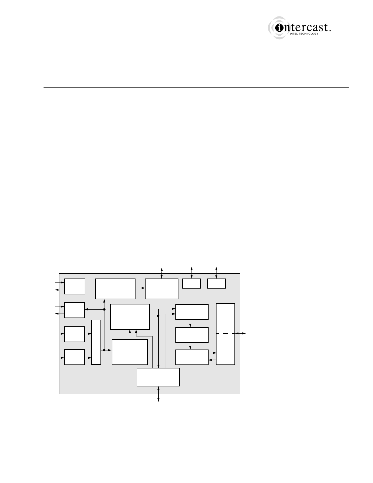
from the continuous video data stream. Figure 1 shows a block diagram of the
Bt848/848A/849A, and Figure 2 shows a detailed block diagram of the decoder
and scaler sections.
The video data input may be scaled, color translated, and burst transferred to a
target location on a field basis. This allows for simultaneous preview of one field
and capture of the other field. Alternatively, Bt848/848A/849A is able to capture
both fields simultaneously or preview both fields simultaneously. The fields may
be interlaced into memory or sent to separate field buffers.
The Bt849A includes all the capability in the Bt848A and adds support for WST
decoding (the encoding method for European based Teletext). The Bt849A implements a significant amount of WST decoding in S/W ensuring a very lo w cost TV
card for use in locations requiring Teletext
See Table 1 for a comparison of the Bt848/848A/849A.
The Bt848/848A/849A fully supports the Intel Intercast technology.
Intel Intercast technology combines the rich programming of television and the
exciting world of the Internet on your PC. Imagine watching a news broadcast and
simultaneously getting a Web page providing a historical perspective. Or viewing
a music video and ordering tickets on the Internet for the band’s next appearance
in your area. Or enjoying a favorite sho w and getting special web pages associated
with that program. Now your PC can let you interact with television in all kinds of
new and exciting ways.
Brooktree
®
L848A_A
1
Page 12

FUNCTIONAL DESCRIPTION
Functional Overview
Single-Chip Video Capture for PCI
Bt848/848A/849A
Table 1. PCI Video Decoder Product Family
Bt848 Bt848A Bt849A
Bt848A Analog Video and
Digital Camera Capture
Over the PCI Bus
Composite, S-Video multi-standard Video
Decoder and PCI bus master
Peaking, single crystal operation, digital camera
support
WST (Teletext) decoding support X
XXX
XX
The Bt848A provides support for digital cameras. The Bt848A includes a digital
camera port providing the ability to perform digital capture when a Bt848A is used
in the development of a video board product. The Bt848A is fully compatible with
the Bt848. The datasheet defines the registers and functionality required for implementing analog video capture support. In order to implement digital video interface, refer to the Digital Video section of the datasheet. Note the majority of the
register settings are identical for both analog and digital video support. The Digital
Video section identifies all changes, additional registers, all changes to the analog
register setting that are required in order to support digital video.
The Bt848A can accept digital video from a multitude of sources including the
Silicon Vision and Logitech video cameras. The digital stream is routed to the high
quality down scaler and color adjustment processing. It is then bus mastered into
system memory or displayed via the graphics frame buffer.
DMA Channels Bt848/848A/849A provides two DMA channels for the odd and even fields, each
controlled by a pixel instruction list. This instruction list is created by the Bt848
device driver and placed in the host memory. The instructions control the transfer
of pixels to target memory locations on a byte resolution basis. Complex clipping
can be accomplished by the instruction list, blocking the generation of PCI bus cycles for pixels that are not to be seen on the display.
The DMA channels can be programmed on a field basis to deliver the video data
in packed or planar format. In packed mode, YCrCb data is stored in a single continuous block of memory. In planar mode, the YCrCb data is separated into three
streams which are burst to different target memory blocks. Having the video data
in planar format is useful for applications where the data compression is accomplished via software and the CPU.
2
L848A_A
Brooktree
®
Page 13
Bt848/848A/849A
Single-Chip Video Capture for PCI
FUNCTIONAL DESCRIPTION
Functional Overview
Figure 1. Bt848/848A/849A Detailed Block Diagram
PCI
Bus
FIFO Data MUX
Address Generator
DMA Controller PCI Initiator
FIFOs
Y: 70x36
Format
Cb: 35x36
MUX
Instruction
Cr: 35x36
Queue
# DWORDS
Instr Data
Wr
Local Registers
PCI
AD MUX
Controller
PCI T arget
PCI
Config
Bus
Parity Generator
Rd
Interrupts
Registers
GPIO
Input
(Digital Video
Bt848A & Bt849A
Only)
Video Data Format Converter
YCrCb 4:2:2, 4:1:1
Video
Video
Video
Analog
8-Bit Dither
CSC/Gamma
Scaler
Decoder
C Master
2
I
GPIO
Brooktree
®
L848A_A
3
Page 14
FUNCTIONAL DESCRIPTION
Functional Overview
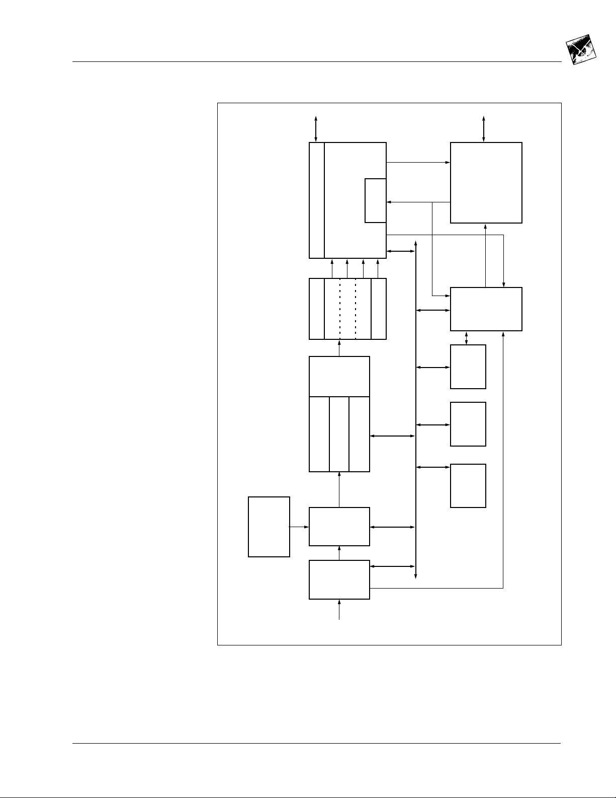
Figure 2. Bt848 Video Decoder and Scaler Block Diagram
(!)
SYNCDET
AGCCAP
REFOUT
MUXOUT
MUX0
MUX1
(2)
MUX2
MUX3
Single-Chip Video Capture for PCI
Bt848/848A/849A
XT1O
XT1I
XT0O
XT0I
and Brightness
Hue, Saturation,
Clocking
Adjust
Horizontal and
YREF+
YIN
YREF–
CLEVEL
CREF+
CIN
CREF–
Y
A/D
C
A/D
AGC and
Sync Detect
Oversampling
Low-Pass Filter
Y/C
Separation
Demod
Chroma
Notes: (1). Bt848 only.
(2). Bt848A and Bt849A only.
PCI Bus Interface Bt848/848A/849A is designed to efficiently utilize the available 132 MB/s PCI
bus. The 32-bit DWORDs are output on the PCI bus with the appropriate image
data under the control of the DMA channels. The video stream consumes bus
bandwidth with average data rates varying from 44 MB/s for full size 768x576
PAL RGB32, to 4.6 MB/s for NTSC CIF 320 x 240 RGB16, to 0.14 MB/s for
NTSC ICON 80 x 60 8-bit mode.
The pixel instruction stream for the DMA channels consumes a minimum of 0.1
MB/s. Achieving high performance throughput on PCI may be a problem with
slow targets and long bus access latencies. The Bt848/848A/849A provides the
means for handling the bandwidth bottlenecks that sometimes occur depending on
a particular system configuration. Bt848/848A/849A’s ability to gracefully degrade and to recover from FIFO overruns to the nearest pix el in real-time is the best
possible solution to these system bottlenecks.
and Scaling
Vertical Filtering
To FIFO Input Data Formatter
4
L848A_A
Brooktree
®
Page 15

Bt848/848A/849A
Single-Chip Video Capture for PCI
FUNCTIONAL DESCRIPTION
Functional Overview
UltraLock The Bt848/848A/849A employs a proprietary technique known as UltraLock to
lock to the incoming analog video signal. It will always generate the required number of pixels per line from an analog source in which the line length can vary by as
much as a few microseconds. UltraLock’ s digital locking circuitry enables the V ideoStream decoders to quickly and accurately lock on to video signals, regardless of
their source. Since the technique is completely digital, UltraLock can recognize
unstable signals caused by VCR headswitches or an y other deviation, and adapt the
locking mechanism to accommodate the source. UltraLock uses nonlinear techniques which are difficult, if not impossible, to implement in genlock systems. And
unlike linear techniques, it adapts the locking mechanism automatically.
Scaling and Cropping The Bt848/848A/849A can reduce the video image size in both horizontal and ver-
tical directions independently using arbitrarily selected scaling ratios. The X and Y
dimensions can be scaled down to one-sixteenth of the full resolution. Horizontal
scaling is implemented with a six-tap interpolation filter while up to 5-tap interpolation is used for vertical scaling with a line store.
The video image can be arbitrarily cropped by reducing the number of active
scan lines and active horizontal pixels per line.
The Bt848/848A/849A supports a temporal decimation feature that reduces
video bandwidth by allowing frames or fields to be dropped from a video sequence
at fixed but arbitrarily selected intervals.
Input Interface Analog video signals are input to the Bt848/848A/849A via a three-input multi-
plexer that can select between three composite source inputs or between two composite and a single S-video input source. When an S-video source is input to the
Bt848/848A/849A, the luma component is fed through the input analog multiplexer, and the chroma component is fed directly into the C input pin. An automatic
gain control circuit enables the Bt848 to compensate for non-standard amplitudes
in the analog signal input. On the Bt848A and Bt849A there is an additional mux
input (providing a four-input multiplexer).
The clock signal interface consists of two pairs of pins for crystal connection
and two clock output pins. One pair of crystal pins is for connection to a 28.64
MHz (8*NTSC Fsc) crystal which is selected for NTSC operation. The other is for
P AL operation with a 35.47 MHz (8*PAL Fsc) crystal. Either fundamental or third
harmonic crystals may be used. Alternatively, CMOS oscillators may be used.
GPIO The Bt848/848A/849A provides a 24-bit general purpose I/O bus. This interface
can be used to input or output up to 24 general purpose I/O signals. Alternatively,
the GPIO port can be used as a means to input or output video decoder data. For example, the Bt848/848A/849A can input the video data from an external video decoder and bypass the Bt848/848A/849A’s internal video decoder block. Another
application is to output the video decoder data from the Bt848/848A/849A over the
GPIO bus for use by external circuitry.
Brooktree
®
L848A_A
5
Page 16

FUNCTIONAL DESCRIPTION
Functional Overview
Single-Chip Video Capture for PCI
Bt848/848A/849A
Vertical Blanking Interval
Data Capture
2
I
C Interface The Bt848/848A/849A provides a two-wire Inter-Integrated Circuit (I2C) inter-
Bt848/848A/849A provides a complete solution for capturing and decoding Vertical Blanking Interval (VBI) data. The Bt848/848A/849A can operate in a VBI Line
Output Mode, in which the VBI data is only captured during select lines. This
mode of operation enables concurrent capture of VBI lines containing ancillary
data and normal video image data.
In addition, the Bt848/848A/849A supports a VBI Frame Output Mode, in
which every line in the video frame is treated as if it was a VBI line. This mode of
operation is designed for use with still frame capture/processing applications.
face. As an I
2
C master, Bt848/848A/849A can program other devices on the video
card, such as a TV tuner. Serial clock and data lines, SCL and SDA are used to
transfer data at a rate of 100 Kbits/s.
6
L848A_A
Brooktree
®
Page 17

Bt848/848A/849A
Single-Chip Video Capture for PCI
FUNCTIONAL DESCRIPTION
Pin Descriptions
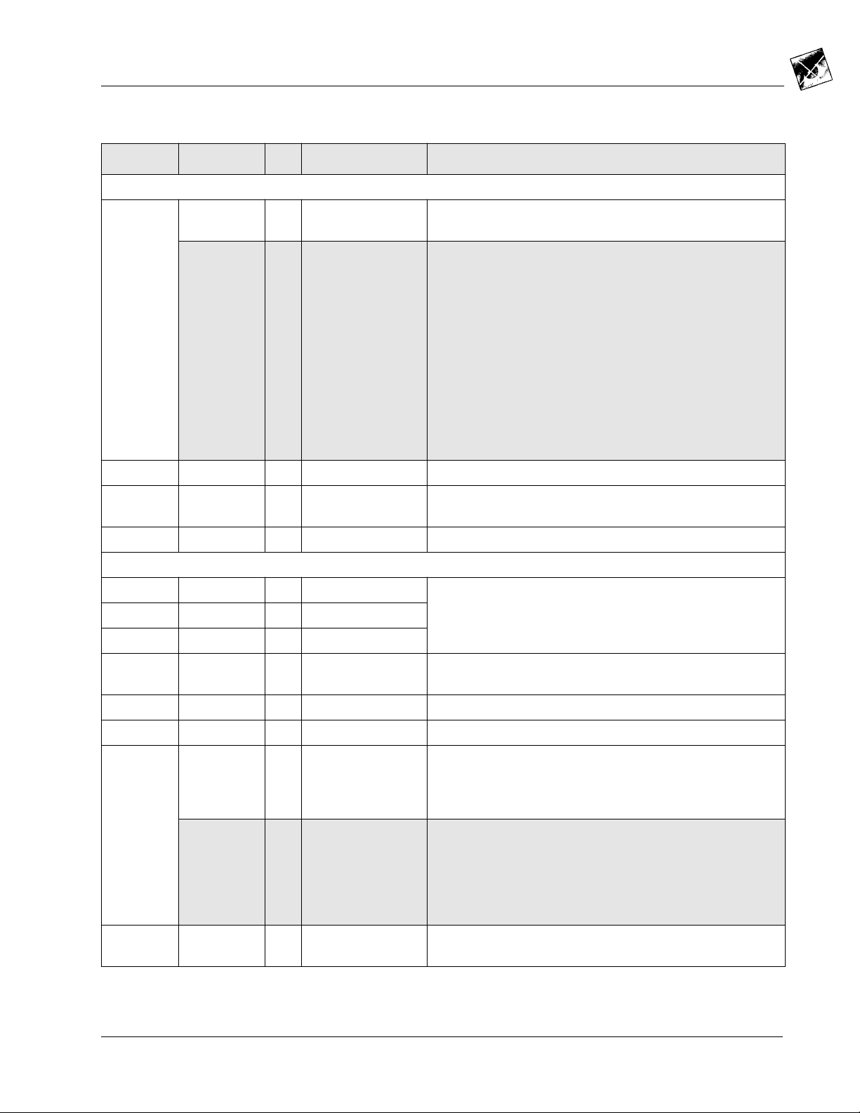
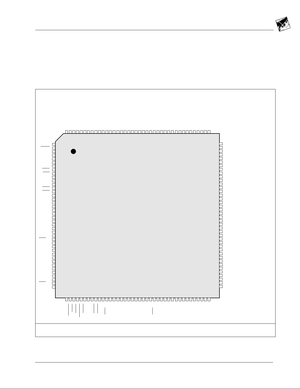
Pin Descriptions
Table 2 provides a description of pin functions, grouped by common function, Table 3 is a list of pin names in
pin-number order, and Figure 3 shows the pinout diagram.
NOTE:
Table 2. Pin Descriptions Grouped by Pin Function
Pins with alternate definitions on the Bt848A and Bt849A are indicated by shading
(1 of 6)
Pin # Pin Name I/O Signal Description
PCI Interface (50 pins)
11 CLK I Clock This input provides timing for all PCI transactions. All PCI sig-
nals except RST and INTA are sampled on the rising edge of
CLK, and all other timing parameters are defined with respect
to this edge. The Bt848 supports a PCI clock of up to
33.333333 MHz.
9 RST I Reset This input three-states all PCI signals asynchronous to the
CLK signal.
13 GNT I Grant Agent granted bus.
28 IDSEL I Initialization Device
Select
15–17,
20–24,
29–32,
35–38,
53–55,
58–62,
66–69,
72–75
AD[31:0] I/O Address/Data These three-state, bi-directional, I/O pins transfer both
This input is used to select the Bt848 during configuration
read and write transactions.
address and data information. A bus transaction consists of
an address phase followed by one or more data phases for
either read or write operations.
The address phase is the clock cycle in which FRAME
first asserted. During the address phase, AD[31:0] contains a
byte address for I/O operations and a DWORD address for
configuration and memory operations. During data phases,
AD[7:0] contains the least significant byte and AD[31:24] contains the most significant byte.
Read data is stable and valid when TRD
write data is stable and valid when IRD
transferred during the clocks when both TRD
asserted.
Y is asserted and
Y is asserted. Data is
Y and IRDY are
is
27, 39,
52, 65
Brooktree
[3:0] I/O Bus Com-
CBE
mand/Byte
Enables
®
These three-state, bi-directional, I/O pins transfer both bus
command and byte enable information. During the address
phase of a transaction, CBE
During the data phase, CBE
The byte enables are valid for the entire data phase and
determine which byte lanes carry meaningful data. CBE
refers to the most significant byte and CBE
least significant byte.
[3:0] contain the bus command.
[3:0] are used as byte enables.
[0] refers to the
L848A_A
[3]
7
Page 18

FUNCTIONAL DESCRIPTION
Pin Descriptions
Single-Chip Video Capture for PCI
Bt848/848A/849A
Table 2. Pin Descriptions Grouped by Pin Function
Pin # Pin Name I/O Signal Description
51 PAR I/O Parity This three-state, bi-directional, I/O pin provides even parity
42 FRAME I/O Cycle Frame This sustained three-state signal is driven by the current
43 IRDY I/O Initiator Ready This sustained three-state signal indicates the bus master’s
(2 of 6)
across AD[31:0] and CBE
of 1’s on PAR, AD[31:0], and CBE
ber.
PAR is stable and valid one clock after the address phase.
For data phases, PAR is stable and valid one clock after
either TRD
write. Once valid, PAR remains valid until one clock after the
completion of the current data phase. PAR and AD[31:0] have
the same timing, but PAR is delayed by one clock. The target
drives PAR for read data phases; the master drives PAR for
address and write data phases.
master to indicate the beginning and duration of an access.
FRAME
tion. Data transfer continues throughout assertion. At deassertion, the transaction is in the final data phase.
readiness to complete the current data phase.
and TRD
clock. During a read, IRD
ready to accept data. During a write, IRD
initiator has placed valid data on AD[31:0]. Wait cycles are
inserted until both IRD
Y is asserted on a read or IRDY is asserted on a
is asserted to signal the beginning of a bus transac-
Y is used in conjunction with TRDY. When both IRDY
IRD
Y are asserted, a data phase is completed on that
[3:0]. This means that the number
[3:0] equals an even num-
Y indicates when the initiator is
Y indicates when the
Y and TRDY are asserted together.
44 TRDY I/O Target Ready This sustained three-state signal indicates the target’s readi-
ness to complete the current data phase.
Y is used in conjunction with TRDY. When both IRDY
IRD
and TRD
clock. During a read, TRD
senting data. During a write, TRD
is ready to accept the data. Wait cycles are inserted until both
IRD
45 DEVSEL I/O Device Select This sustained three-state signal indicates device selection.
When actively driven, DEVSEL
has decoded its address as the target of the current access.
46 STOP I/O Stop This sustained three-state signal indicates the target is
requesting the master to stop the current transaction.
49 PERR I/O Parity Error Report data parity error.
14 REQ O Request Agent desires bus.
8 INTA O Interrupt A This signal is an open drain interrupt output.
50 SERR O System Error Report address parity error. Open drain.
See PCI Specification 2.1 for further documentation
Y are asserted, a data phase is completed on that
Y indicates when the target is pre-
Y indicates when the target
Y and TRDY are asserted together.
indicates the driving device
8
L848A_A
Brooktree
®
Page 19
Bt848/848A/849A
Single-Chip Video Capture for PCI
FUNCTIONAL DESCRIPTION
Pin Descriptions
Table 2. Pin Descriptions Grouped by Pin Function
Pin # Pin Name I/O Signal Description
General Purpose I/O (27 pins)
82–89,
92–99,
110–117
119 GPINTR I GP Interrupt GP port requests an interrupt. Internally pulled up to VDDG.
118 GPWE I GP Write Enable GP port write enable for registered inputs. Internally pulled up
GPIO[23:0] I/O General Purpose
I/O
GPIO[23]
GPIO[22]
GPIO[21]
GPIO[20]
GPIO[19]
GPIO[18]
GPIO[17]
GPIO[16]
GPIO[9]
GPIO[8]
GPIO[7:0]
O
Clkx1
O
Field
O
Vactive
O
Vsync
O
Hactive
O
Hsync
O
Composite Active
O
Composite Sync
I
Vsync/Field
I
Hsync
I
Video Data Input at
GPCLK = CLKX2
rate
(3 of 6)
24 bits of programmable I/O. These pins are internally pulled
up to VDDG.
Bt848A and Bt849A pin decoding when in digital video input
and SPI mode.
to VDDG.
108 GPCLK I/O GP Clock Video clock. Internally pulled up to VDDG.
Input Stage (14 pins)
141 MUX0 I Analog composite video inputs to the on-chip input multi143 MUX1 I
145 MUX2 I
139 MUXOUT O The analog video output of the 3 to 1 multiplexer. Must con-
138 YIN I The analog composite or luma input to theY-ADC.
154 CIN I The analog chroma input to the C-ADC.
147 SYNCDET I The sync stripper input used to generate timing information
MUX3 I In the Bt848A and Bt849A the SYNCDET is not required and
131 AGCCAP A The AGC time constant control capacitor node. Must be con-
plexer. Used to select between three composite sources or
two composite and one S-video source. Unused pins should
be connected to ground.
nect to the YIN pin.
for the AGC circuit. Must be connected through a 0.1 µF
capacitor to the same source as the Y-ADC. A 1 MΩ bleeder
resistor should be connected to ground.
is used as a fourth mux input.
Analog composite video inputs to the on-chip input multiplexer. Used to select between three composite sources or
two composite and one S-video source. Unused pins should
be connected to ground.
nected to a 0.1 µF capacitor to ground.
Brooktree
®
L848A_A
9
Page 20
FUNCTIONAL DESCRIPTION
Pin Descriptions
Single-Chip Video Capture for PCI
Bt848/848A/849A
Table 2. Pin Descriptions Grouped by Pin Function
Pin # Pin Name I/O Signal Description
133 REFOUT O Output of the AGC which drives the YREF+ and CREF+ pins.
REFOUT O In the Bt848Aand Bt849A, the external 30 K, 30 K, and 2 K
137 YREF+ I The top of the reference ladder of the Y-ADC. This should be
150 YREF– I The bottom of the reference ladder of the Y-ADC. This should
151 CREF+ I The top of the ref erence ladder of the C-ADC. This should be
157 CREF– I The bottom of the reference ladder of the C-ADC . This should
158 CLEVEL I An input to provide the DC level reference for the C-ADC.
CLEVEL I In the Bt848A and Bt849A, this input is internally generated.
(4 of 6)
resistors are not required. However, the 0.1 µF capacitor
ground to GND is still needed (see Figure 25).
connected to REFOUT.
be connected to analog ground (AGND).
connected to REFOUT.
be connected to analog ground (AGND).
This voltage should be one half of CREF+.
No external components are required.
2
C Interface (2 pins)
I
78 SCL I/O Serial Clock Bus clock, output open drain.
79 SDA I/O Serial Data Bit Data or Acknowledge, output open drain.
Video Timing Clock Interface (5 pins)
102 XT0I A Clock Zero pins. A 28.636363 MHz (8*Fsc) fundamental (or
103 XT0O A
XT0I A In the Bt848A and Bt849A, this is the only clock source
XT0O A
105 XT1I A Clock One pins. A 35.468950 MHz (8*Fsc) fundamental (or
106 XT1O A
third harmonic) crystal can be tied directly to these pins, or a
single-ended oscillator can be connected to XT0I. CMOS
level inputs must be used. This clock source is selected for
NTSC input sources. When the chip is configured to decode
PAL but not NTSC (and therefore only one clock source is
needed), the 35.468950 MHz source is connected to this port
(XT0).
required to decode all video formats. If only one source is
used the frequency must be 28.636363 MHz (50 ppm) and a
series resistor must be added to the layout. Alternatively, the
Bt848A and Bt849A may be configured exactly as the Bt848
(using 28.636363 and 35.468950 MHz sources).
third harmonic) crystal can be tied directly to these pins, or a
single-ended oscillator can be connected to XT1I. CMOS
level inputs must be used. This clock source is selected for
PAL input sources. If either NTSC or PAL is being decoded,
and therefore only XT0I and XT0O are connected to a crystal,
must
XT1I should be tied either high or low, and XT1O
floating.
be left
10
L848A_A
Brooktree
®
Page 21

Bt848/848A/849A
Single-Chip Video Capture for PCI
FUNCTIONAL DESCRIPTION
Pin Descriptions
Table 2. Pin Descriptions Grouped by Pin Function
Pin # Pin Name I/O Signal Description
104 NUMXTAL I Crystal Format Pin. This pin is set to indicate whether one or
3 TCK I Test clock. Used to synchronize all JTAG test structures.
5 TMS I Test Mode Select. JTAG input pin whose transitions drive the
7 TDI I Test Data Input. JTAG pin used for loading instructions to the
6 TDO O Test Data Output. JTAG pin used for verifying test results of
(5 of 6)
two crystals are present so that the Bt848 can select XT1 or
XT0 as the default in auto format mode. A logical zero on this
pin indicates one crystal is present. A logical one indicates
two crystals are present. This pin is internally pulled up to
VDDG.
JTAG (5 pins)
When JTAG operations are not being performed, this pin
must be driven to a logical low.
JTAG state machine through its sequences. When JTAG
operations are not being performed, this pin must be left floating or tied high.
TAP controller or for loading test vector data for boundary-scan operation. When JTAG operations are not being
performed, this pin must be left floating or tied high.
all JTAG sampling operations. This output pin is active for
certain JTAG operations and will be three-stated at all other
times.
2 TRST I Test Reset. JTAG pin used to initialize the JTAG controller.
This pin is tied low for normal device operation. When pulled
high, the JTAG controller is ready for device testing.
Note:
Not all PCs drive the PCI bus TRST pin. In these
pin on the Bt848 board is connected
1, 18, 40,
63, 81,
101, 120
130, 134,
136, 148,
152, 156
10, 25,
33, 47,
56, 70, 76
computers, if the TRST
to TRST
power up in an undefined state. In these designs, the TRST
pin on the Bt848 card must be tied low (disabling JTAG).
Power & Ground (57 pins)
VDD +5V P Power supply for digital circuitry. All VDD pins must be con-
nected together as close to the device as possible. A 0.1 µF
capacitor should be connected between each group of VDD
pins and the ground plane as close to the device as possible.
VAA +5V
VPOS +5V
VDDP
PCI VIO
P Power supply for analog circuitry. All VAA pins and VPOS
must be connected together as close to the device as possible. A 0.1 µF ceramic capacitor should be connected
between each group of VAA pins and the ground plane as
close to the device as possible.
P P o w er supply for PCI bus signals. A 0.1 µF ceramic capacitor
should be connected between the VDDP pins and the ground
plane as close to the device as possible.
on the PCI bus (which is not driven) the Bt848 may
Brooktree
®
L848A_A
11
Page 22
FUNCTIONAL DESCRIPTION
Pin Descriptions
Single-Chip Video Capture for PCI
Bt848/848A/849A
Table 2. Pin Descriptions Grouped by Pin Function
Pin # Pin Name I/O Signal Description
90, 109,
123
12, 19,
26, 34,
41, 48,
57, 64,
71, 77,
80, 91,
100, 107,
121, 122,
160
132, 135,
140, 142,
144, 146,
149, 153,
155, 159
4 PVREF A This pin should be connected to GND (this reference signal
VDDG +5V P Power supply for GPIO port signals. A 0.1 µF ceramic capac-
GND G Ground for digital circuitry. All GND pins must be connected
AGND,
VNEG
G Ground for analog circuitry. All AGND pins and VNEG must
(6 of 6)
itor should be connected between the VDDG pins and the
ground plane as close to the device as possible.
together as close to the device as possible.
be connected together as close to the device as possible.
may be connected to the +3.3 V pin on the PCI bus, even if
the PCI bus does not supply 3.3 V).
124–129 N/C No connect Reserved
GPX[5:0] I/O Remapped from
GPIO [5:0]
I/O Column Legend:
I = Digital Input
O = Digital Output
I/O = Digital Bidirectional
A = Analog
G = Ground
P = Power
These pins are remapped on the Bt848A and Bt849A to provide the same functionality as on the Bt848 but on a different
pin.
12
L848A_A
Brooktree
®
Page 23
Bt848/848A/849A
Single-Chip Video Capture for PCI
Pin Assignments
Figure 3. Bt848/848A/849A Pinout Diagram
GND
AGND
CLEVEL
CREF–
VAA
AGND
CIN
AGND
VAA
CREF+
YREF–
AGND
VAA
SYNCDET (MUX3)
AGND
146
147
148
149
150
151
152
153
154
155
156
157
158
159
160
1
VDD
TCK
TMS
TDO
TDI
INT
RST
CLK
GNT
VDD
VDD
2
3
4
5
6
7
8
A
9
10
11
12
13
14
15
16
17
18
19
20
21
22
23
24
25
26
[3]
27
28
29
30
31
32
33
34
35
36
37
38
[2]
39
40
48
47
46
45
44
43
42
41
Bt848/848A/849A
55
54
53
52
51
50
49
TRST
PVREF
VDDP
GND
REQ
AD[31]
AD[30]
AD[29]
GND
AD[28]
AD[27]
AD[26]
AD[25]
AD[24]
VDDP
GND
CBE
IDSEL
AD[23]
AD[22]
AD[21]
AD[20]
VDDP
GND
AD[19]
AD[18]
AD[17]
AD[16]
CBE
MUX2
AGND
144
145
57
56
MUX1
AGND
142
143
59
58
MUX0
AGND
140
141
61
60
MUXOUT
YIN
YREF+
137
138
139
64
63
62
VAA
136
65
AGND
135
66
VAA
REFOUT
133
134
68
67
VNEG
AGCCAP
131
132
70
69
VPOS
N/C (GPX0)
N/C (GPX1)
128
129
130
73
72
71
N/C (GPX2)
N/C (GPX3)
N/C (GPX4)
N/C (GPX5)
124
125
126
127
77
76
75
74
VDDG
GND
122
123
79
78
FUNCTIONAL DESCRIPTION
Pin Assignments
GND
121
120
VDD
119
GPINTR
118
GPWE
117
GPIO[0]
116
GPIO[1]
115
GPIO[2]
GPIO[3]
114
GPIO[4]
113
GPIO[5]
112
GPIO[6]
111
GPIO[7]
110
VDDG
109
GPCLK
108
GND
107
XT1O
106
XT1I
105
NUMXTAL
104
XT0O
103
XT0I
102
VDD
101
GND
100
GPIO[8] (HSYNC)
99
GPIO[9] (VSYNC/FIELD)
98
GPIO[10]
97
GPIO[11]
96
GPIO[12]
95
GPIO[13]
94
GPIO[14]
93
GPIO[15]
92
GND
91
VDDG
90
GPIO[16] (Composite SYNC)
89
GPIO[17] (Composite ACTIVE)
88
GPIO[18] (HSYNC)
87
GPIO[19] (HACTIVE)
86
GPIO[20] (VSYNC)
85
GPIO[21] (VACTIVE)
84
GPIO[22] (FIELD)
83
GPIO[23] (CLKX1)
82
VDD
81
80
GND
FRAME
IRDY
TRDY
DEVSEL
STOP
GND
VDDP
PERR
SERR
PAR
CBE
AD[15]
AD[14]
VDDP
AD[13]
GND
AD[12]
AD[11]
AD[10]
AD[9]
AD[8]
VDD
GND
[1]
Note: Bt848A and Bt849A pin alternate definitions indicated in ().
Brooktree
®
L848A_A
[0]
CBE
AD[7]
AD[6]
AD[5]
AD[4]
GND
VDDP
AD[3]
AD[2]
AD[1]
AD[0]
GND
VDDP
SCL
SDA
GND
13
Page 24
FUNCTIONAL DESCRIPTION
Pin Assignments
Table 3. Bt848 Pin List
Single-Chip Video Capture for PCI
Bt848/848A/849A
Pin
#
1 VDD 33 VDDP 65 CBE
2 TRST 34 GND 66 AD[7] 98 GPIO[9]
3 TCK 35 AD[19] 67 AD[6] 99 GPIO[8]
Pin
Name
Pin
#
Pin
Name
Pin
#
Pin
Name
Pin
#
Pin
Name
Pin
#
[0] 97 GPIO[10] 129 N/C
(1)
(1)
130 VPOS
131 AGCCAP
Pin
Name
(1)
4 PVREF 36 AD[18] 68 AD[5] 100 GND 132 VNEG
5 TMS 37 AD[17] 69 AD[4] 101 VDD 133 REFOUT
6 TDO 38 AD[16] 70 VDDP 102 XT0I 134 VAA
7 TDI 39 CBE[2] 71 GND 103 XT0O 135 AGND
8 INTA 40 VDD 72 AD[3] 104 NUMXTAL 136 VAA
9 RST 41 GND 73 AD[2] 105 XT1I 137 YREF+
10 VDDP 42 FRAME 74 AD[1] 106 XT1O 138 YIN
11 CLK 43 IRDY 75 AD[0] 107 GND 139 MUXOUT
12 GND 44 TRDY 76 VDDP 108 GPCLK 140 AGND
13 GNT 45 DEVSEL 77 GND 109 VDDG 141 MUX0
14 REQ 46 STOP 78 SCL 110 GPIO[7] 142 AGND
15 AD[31] 47 VDDP 79 SDA 111 GPIO[6] 143 MUX1
16 AD[30] 48 GND 80 GND 112 GPIO[5] 144 AGND
17 AD[29] 49 PERR 81 VDD 113 GPIO[4] 145 MUX2
18 VDD 50 SERR 82 GPIO[23]
19 GND 51 PAR 83 GPIO[22]
20 AD[28] 52 CBE[1] 84 GPIO[21]
21 AD[27] 53 AD[15] 85 GPIO[20]
22 AD[26] 54 AD[14] 86 GPIO[19]
23 AD[25] 55 AD[13] 87 GPIO[18]
24 AD[24] 56 VDDP 88 GPIO[17]
25 VDDP 57 GND 89 GPIO[16]
(1)
114 GPIO[3] 146 AGND
(1)
115 GPIO[2] 147 SYNCDET
(1)
116 GPIO[1] 148 VAA
(1)
117 GPIO[0] 149 AGND
(1)
118 GPWE 150 YREF–
(1)
119 GPINTR 151 CREF+
(1)
120 VDD 152 VAA
(1)
121 GND 153 AGND
26 GND 58 AD[12] 90 VDDG 122 GND 154 CIN
27 CBE[3] 59 AD[11] 91 GND 123 VDDG 155 AGND
28 IDSEL 60 AD[10] 92 GPIO[15] 124 N/C
29 AD[23] 61 AD[9] 93 GPIO[14] 125 N/C
30 AD[22] 62 AD[8] 94 GPIO[13] 126 N/C
31 AD[21] 63 VDD 95 GPIO[12] 127 N/C
32 AD[20] 64 GND 96 GPIO[11] 128 N/C
(1)
(1)
(1)
(1)
(1)
156 VAA
157 CREF–
158 CLEVEL
159 AGND
160 GND
(1)
Notes: (1). Alternate pin definitions on Bt848A and Bt849A.
14
L848A_A
Brooktree
®
Page 25

Bt848/848A/849A
Single-Chip Video Capture for PCI
The Challenge The line length (the interval between the midpoints of the falling edges of succeed-
FUNCTIONAL DESCRIPTION
UltraLock
UltraLock
ing horizontal sync pulses) of analog video sources is not constant. For a stable
source such as studio quality source or test signal generators, this variation is very
small: ±2 ns. However, for an unstable source such as a VCR, laser disk player, or
TV tuner, line length variation is as much as a few microseconds.
Digital display systems require a fixed number of pixels per line despite these
variations. The Bt848 employs a technique known as UltraLock to implement
locking to the horizontal sync and the subcarrier of the incoming analog video signal and generating the required number of pixels per line.
Operation Principles of
UltraLock
UltraLock is based on sampling using a fixed-frequency, stable clock. Since the
video line length will vary , the number of samples generated using a fixed-frequency sample clock will also vary from line to line. If the number of generated samples
per line is always greater than the number of samples per line required by the particular video format, the number of acquired samples can be reduced to fit the required number of pixels per line.
The Bt848 requires an 8*Fsc (28.64 MHz for NTSC and 35.47 MHz for PAL)
crystal or oscillator input signal source. The 8*Fsc clock signal, or CLKx2, is divided down to CLKx1 internally (14.32 MHz for NTSC and 17.73 MHz for PAL).
CLKx2 and CLKx1 are internal signals and are not made available to the system.
UltraLock operates at CLKx1 although the input waveform is sampled at CLKx2
then low pass filtered and decimated to CLKx1 sample rate.
At a 4*Fsc (CLKx1) sample rate there are 910 pixels for NTSC and 1,135 pixels
for PAL/SECAM within a nominal line time interval (63.5 µs for NTSC and 64 µs
for PAL/SECAM). For square pixel NTSC and PAL/SECAM formats, there
should only be 780 and 944 pixels per video line, respectively. This is because the
square pixel clock rates are slower than a 4*Fsc clock rate, i.e., 12.27 MHz for
NTSC and 14.75 MHz for PAL.
UltraLock accommodates line length variations from nominal in the incoming
video by always acquiring more samples, at an effective 4*Fsc rate, than are required by the particular video format and outputting the correct number of pixels
per line. UltraLock then interpolates the required number of pixels in a way that
maintains the stability of the original image despite variation in the line length of
the incoming analog waveform.
Brooktree
®
L848A_A
15
Page 26
FUNCTIONAL DESCRIPTION
UltraLock
Single-Chip Video Capture for PCI
Bt848/848A/849A
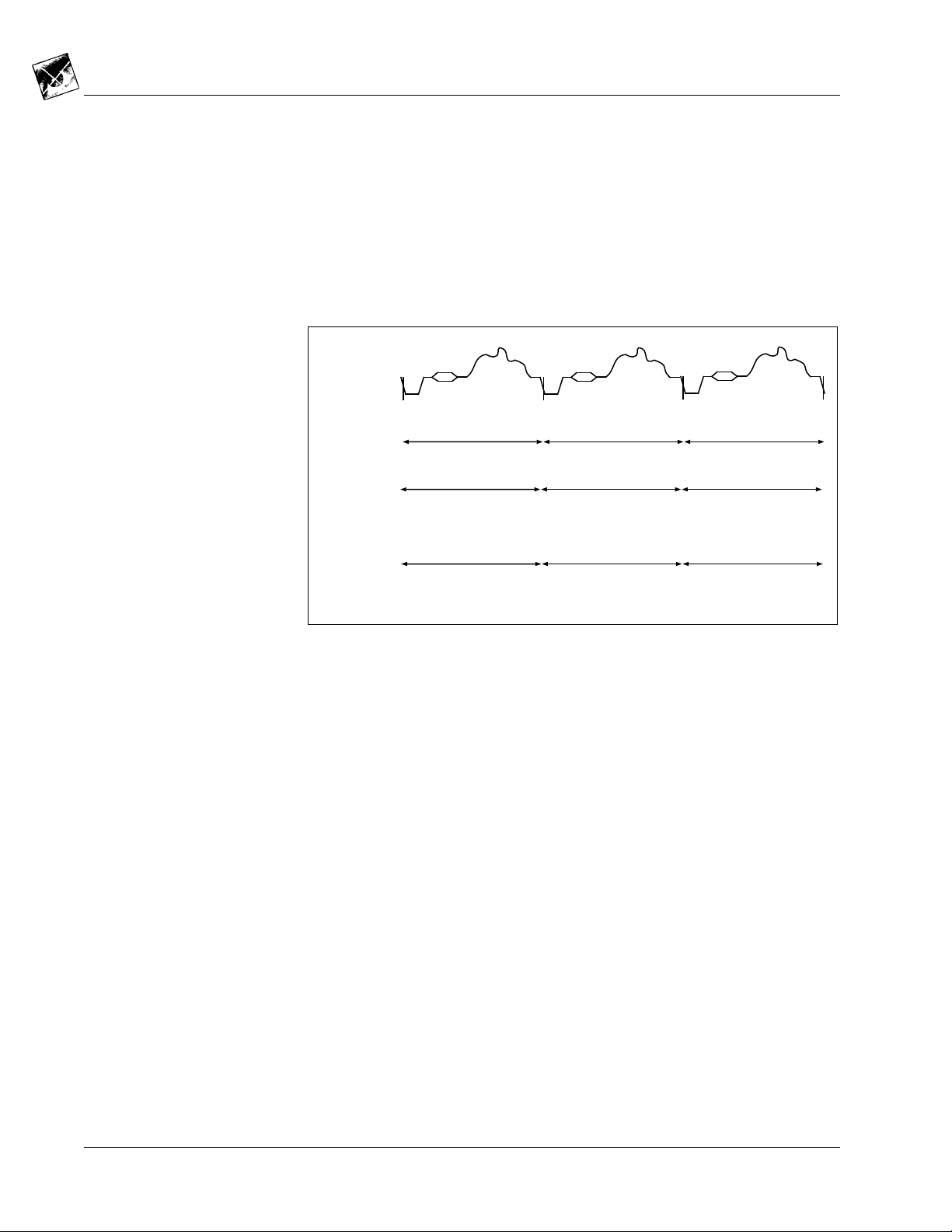
The example illustrated in Figure 4 shows three successive lines of video being
decoded for square pixel NTSC output. The first line is shorter than the nominal
NTSC line time interval of 63.5 µs. On this first line, a line time of 63.2 µs sampled
at 4*Fsc (14.32 MHz) generates only 905 pixels. The second line matches the
nominal line time of 63.5 µs and provides the expected 910 pixels. Finally, the
third line is too long at 63.8 µs within which 913 pixels are generated. In all three
cases, UltraLock outputs only 780 pixels.
Figure 4. UltraLock Behavior for NTSC Square Pixel Output
Analog
Waveform
Line
Length
Pixels
Per Line
Pixels
Sent to
the FIFO
by
UltraLock
63.2 µs
905 pixels
780 pixels
63.5 µs
910 pixels
780 pixels
63.8 µs
913 pixels
780 pixels
UltraLock can be used to extract any programmable number of pixels from the
original video stream as long as the sum of the nominal pixel line length (910 for
NTSC and 1,135 for PAL/SECAM) and the worst case line length variation from
nominal in the active region is greater than or equal to the required number of output pixels per line, i.e.,
P
where: P
Nom
+P
NomPVar
= Nominal number of pixels per line at 4*Fsc sample rate
≥
Desired
(910 for NTSC, 1,135 for PAL/SECAM)
P
= Variation of pixel count from nominal at 4*Fsc (can be a
Var
positive or negative number)
P
= Desired number of output pixels per line
Desired
16
It should be noted that, for stable inputs, UltraLock guarantees the time between
the falling edges of HRESET only to within one pixel. UltraLock does, however,
guarantee the number of active pixels in a line as long as the above relationship
holds.
L848A_A
Brooktree
®
Page 27
Bt848/848A/849A
Single-Chip Video Capture for PCI
FUNCTIONAL DESCRIPTION
Composite Video Input Formats
Composite Video Input Formats
Bt848 supports several composite video input formats. Table 4 shows the different
video formats and some of the countries in which each format is used.
Table 4. Video Input Formats Supported by the Bt848
Format Lines Fields F
NTSC-M 525 60 3.58 MHz
NTSC-Japan
PAL-B 625 50 4.43 MHz
PAL-D 625 50 4.43 MHz
PAL-G 625 50 4.43 MHz
PAL-H 625 50 4.43 MHz
PAL-I 625 50 4.43 MHz
PAL-M 525 60 3.58 MHz
PAL-N Combination 625 50 3.58 MHz
PAL-N 625 50 4.43 MHz
SECAM 625 50 4.43 MHz
Notes:(1). NTSC-Japan has 0 IRE setup.
(1)
525 60 3.58 MHz
SC
The video decoder must be programmed appropriately for each of the composite video input formats. Table 5 lists the register values that need to be programmed
for each input format.
L848A_A
17
Page 28

FUNCTIONAL DESCRIPTION
Composite Video Input Formats
Table 5. Register Values for Video Input Formats
Single-Chip Video Capture for PCI
Bt848/848A/849A
Register Bit NTSC-M NTSC-Japan
IFORM
(0x01)
XTSEL
[4:3]
FORMAT
01 01 10 01 10 01 10
001 010 011 100 101 111 110
PAL-B, D,
G, H, I
PAL-M PAL-N
PAL-N
Combination
SECAM
[2:0]
Cropping:
HDELAY,
VDELAY,
VACTIVE,
[7:0] in all
five
registers
Set to desired
cropping
values in
registers
Set to NTSC-M
square pixel
values
Set to desired
cropping
values in
registers
Set to NTSC-M
square pixel
values
Set to PAL-B, D, G, H, I square pixel
values
CROP
HSCALE
[15:0] 0x02AC 0x02AC 0x033C 0x02AC 0x033C 0x033C
(1)
0x033C
(0x08,
0x09)
ADELAY
[7:0] 0x68 0x68 0x7F 0x68 0x7F 0x7F 0x7F
(0x18)
BDELAY
[7:0] 0x5D 0x5D 0x72 0x5D 0x72 0x72 tbd
(0x19)
Notes: (1). The Bt848A and Bt849A will not output square pixel resolution for PAL N-combination. A smaller number of pixels
must be output.
18
L848A_A
Brooktree
®
Page 29
Bt848/848A/849A
Single-Chip Video Capture for PCI
Y/C Separation and Chroma Demodulation
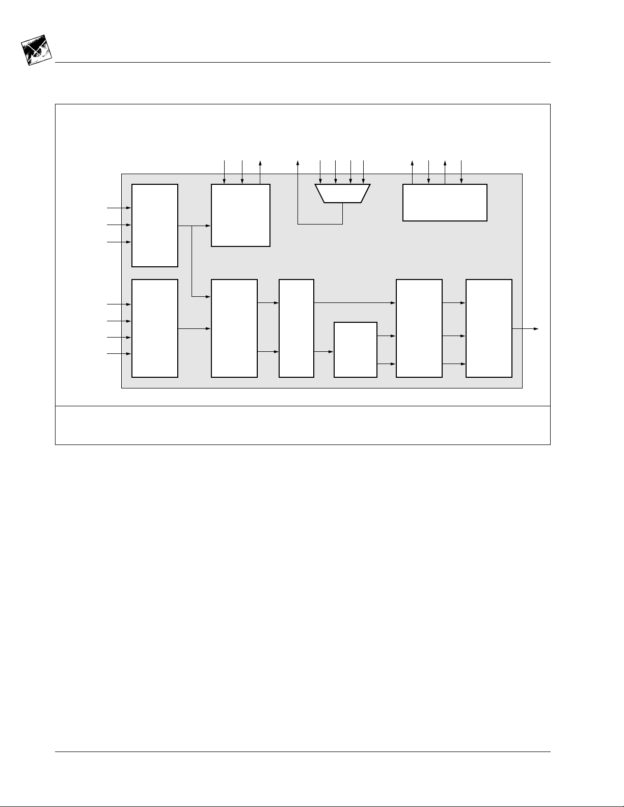
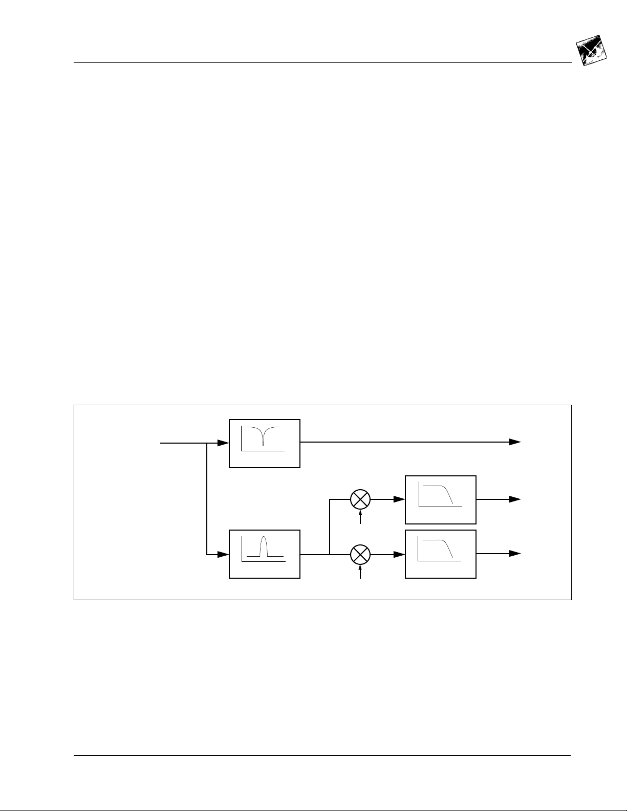
Y/C separation and chroma decoding are handled as shown in Figure 5. Bandpass
and notch filters are implemented to separate the composite video stream. The filter responses are shown in Figure 6. The optional chroma comb filter is implemented in the vertical scaling block. See the Video Scaling, Cropping, and
Temporal Decimation section in this chapter.
Figure 7 schematically describes the filtering and scaling operations.
In addition to the Y/C separation and chroma demodulation illustrated in
Figure 5, the Bt848 also supports chrominance comb filtering as an optional filtering stage after chroma demodulation. The chroma demodulation generates baseband I and Q (NTSC) or U and V (PAL/SECAM) color difference signals.
For S-Video operation, the digitized luma data bypasses the Y/C separation
block completely, and the digitized chrominance is passed directly to the chroma
demodulator.
For monochrome operation, the Y/C separation block is also bypassed, and the
saturation registers (SAT_U and SAT_V) are set to zero.
Figure 5. Y/C Separation and Chroma Demodulation for Composite Video
Y/C Separation and Chroma Demodulation
FUNCTIONAL DESCRIPTION
Composite
Notch Filter
Band Pass Filter
Y
U
Low Pass Filter
sin
V
Low Pass Filter
cos
Brooktree
®
L848A_A
19
Page 30
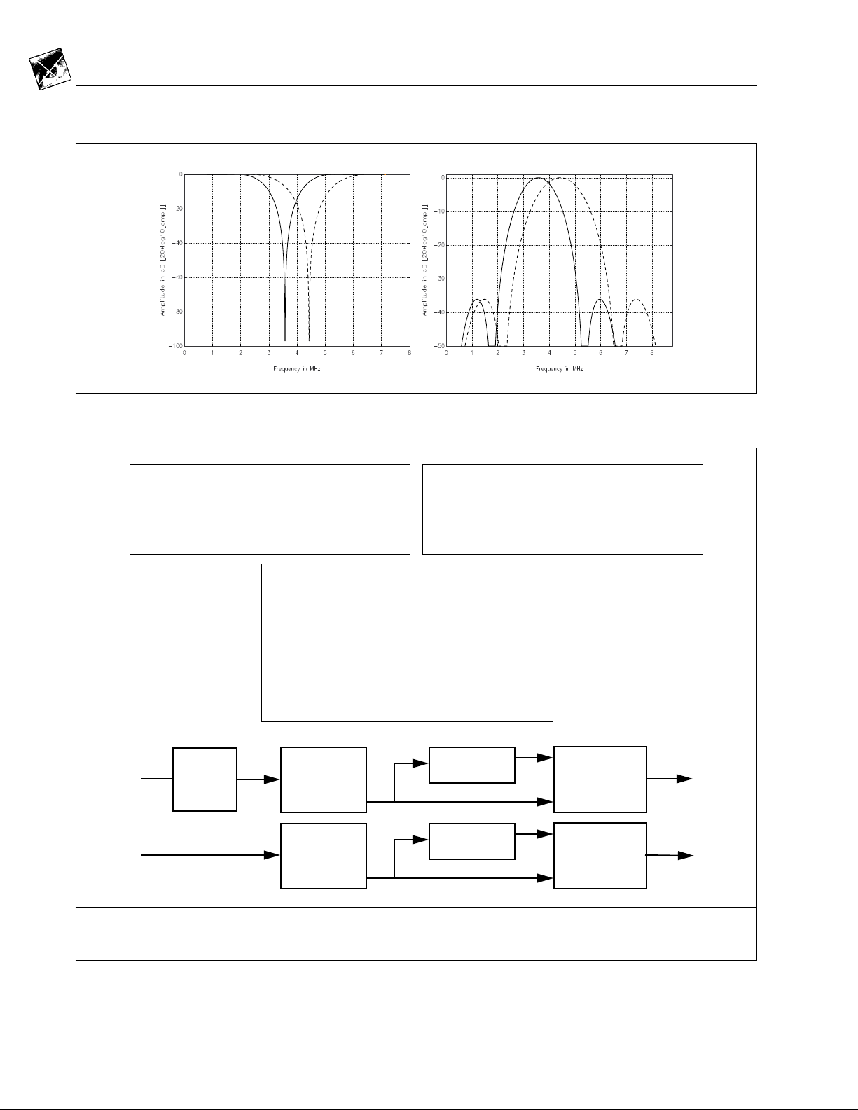
FUNCTIONAL DESCRIPTION
Y/C Separation and Chroma Demodulation
Figure 6. Y/C Separation Filter Responses
Single-Chip Video Capture for PCI
Bt848/848A/849A
Luma Notch Filter Frequency Responses for NTSC and PAL/SECAM
Figure 7. Filtering and Scaling
Horizontal Scaler
Luminance
ABZ1–CZ2–DZ3–EZ4–FZ
+++++=
Chrominance GHZ
NTSC
PAL/SECAM
1–
+=
Chroma Band Pass Filter Frequency Responses for NTSC and PAL/SECAM
NTSC
Vertical Scaler
5–
Luminance CDZ
Chrominance
+=
1
-- 2
1
-- -Z1–+=
2
PAL/SECAM
1–
(Chroma Comb)
Vertical Filter Options
Luminance
Optional
Y Y
3 MHz
Horizontal
Low Pass
Filter
C
6 Tap, 32 Phase
Interpolation
and
Horizontal
Scaling
2 Tap, 32 Phase
Interpolation
and
Horizontal
Scaling
1
-- -1 z1–+()=
2
1
-- -1 2
4
1
-- -1 3
8
1
------ 1 4
16
1–
Z
++()=
Z
+++()=
Z
++++()=
2–
1Z
1–
3Z2–1Z
1–
6 Z2–4 Z
On-chip Memory
On-chip Memory
3–
3–
4–
Z
Luma Comb
Vertical Scaling
Vertical Filtering
Chroma Comb
and
Vertical Scaling
C
Note: Z–1 refers to a pixel delay in the horizontal direction, and a line delay in the vertical direction. The coefficients
are determined by UltraLock and the scaling algorithm
20
L848A_A
Brooktree
®
Page 31

Bt848/848A/849A
Single-Chip Video Capture for PCI
Video Scaling, Cropping, and Temporal Decimation
FUNCTIONAL DESCRIPTION
Video Scaling, Cropping, and Temporal Decimation
The Bt848 provides three mechanisms to reduce the amount of video pixel data in
its output stream; down-scaling, cropping, and temporal decimation. All three can
be controlled independently.
Horizontal and Vertical
Scaling
The Bt848 provides independent and arbitrary horizontal and vertical down scaling. The maximum scaling ratio is 16:1 in both X and Y dimensions. The maximum vertical scaling ratio is reduced from 16:1 when using frames to 8:1 when
using fields. The different methods utilized for scaling luminance and chrominance are described in the following sections.
Luminance Scaling The first stage in horizontal luminance scaling is an optional pre-filter which pro-
vides the capability to reduce anti-aliasing artifacts. It is generally desirable to limit the bandwidth of the luminance spectrum prior to performing horizontal scaling
because the scaling of high-frequency components may create image artifacts in
the resized image. The optional low pass filters shown in Figure 8 reduce the horizontal high-frequency spectrum in the luminance signal. Figure 9 and Figure 10
show the combined results of the optional low-pass filters, the luma notch filter and
the 2x oversampling filter. Figure 12 shows the combined responses of the luma
notch filter and the 2x oversampling filter.
The Bt848 implements horizontal scaling through poly-phase interpolation.
The Bt848 uses 32 different phases to accurately interpolate the value of a pixel.
This provides an effective pixel jitter of less than 6 ns.
In simple pixel- and line-dropping algorithms, non-integer scaling ratios introduce a step function in the video signal that effectively introduces high-frequency
spectral components. Poly-phase interpolation accurately interpolates to the correct pixel and line position providing more accurate information. This results in
aesthetically pleasing video as well as higher compression ratios in bandwidth limited applications.
For vertical scaling, the Bt848 uses a line store to implement four different filtering options. The filter characteristics are shown in Figure 11. The Bt848 provides up to 5-tap filtering to ensure removal of aliasing artifacts.
The number of taps in the vertical filter is set by the VTC register. The user may
select 2, 3, 4 or 5 taps. The number of taps must be chosen in conjunction with the
horizontal scale factor in order to ensure the needed data can fit in the internal
FIFO (see the VFILT bits in the VTC register for limitations). As the scaling ratio
is increased, the number of taps available for vertical scaling is increased. In addition to low-pass filtering, vertical interpolation is also employed to minimize artifacts when scaling to non-integer scaling ratios.
Brooktree
®
L848A_A
21
Page 32

FUNCTIONAL DESCRIPTION
Video Scaling, Cropping, and Temporal Decimation
Single-Chip Video Capture for PCI
Bt848/848A/849A
Figure 8. Optional Horizontal Luma Low-Pass Filter Responses
NTSC PAL/SECAM
QCIF
QCIF
ICON
CIF ICON
CIF
Figure 9. Combined Luma Notch, 2x Oversampling and Optional Low-Pass Filter Response (NTSC)
QCIF
ICON
CIF
Full Spectrum
ICON
QCIF
Pass Band
CIF
Figure 10. Combined Luma Notch, 2x Oversampling and Optional Low-Pass Filter Response (PAL/SECAM)
ICON
QCIF
CIF
Full Spectrum
ICON
QCIF
Pass Band
CIF
22
L848A_A
Brooktree
®
Page 33

Bt848/848A/849A
Single-Chip Video Capture for PCI
Figure 11. Frequency Responses for the Four Optional Vertical Luma Low-Pass Filters
Video Scaling, Cropping, and Temporal Decimation
2-tap
3-tap
4-tap
5-tap
FUNCTIONAL DESCRIPTION
Figure 12. Combined Luma Notch and 2x Oversampling Filter Response
PAL/SECAM
NTSC
Brooktree
®
L848A_A
23
Page 34

FUNCTIONAL DESCRIPTION
Video Scaling, Cropping, and Temporal Decimation
Single-Chip Video Capture for PCI
Bt848/848A/849A
Peaking (Bt848A and
Bt849A Only)
The Bt848A enables four different peaking levels by programming the PEAK bit
and HFILT bits in the SCLOOP register. The filters are shown in Figures 13
and 14.
Figure 13. Peaking Filters (Bt848A/849A only)
HFILT = 00
HFILT = 01
HFILT = 10
HFILT = 11
24
Enhanced Resolution of Passband
HFILT = 10
HFILT = 11
L848A_A
HFILT = 00
HFILT = 01
Brooktree
®
Page 35

Bt848/848A/849A
Single-Chip Video Capture for PCI
Video Scaling, Cropping, and Temporal Decimation
FUNCTIONAL DESCRIPTION
Figure 14. Luma Peaking Filters with 2x Oversampling Filter and Luma Notch (Bt848A/849A only)
HFILT = 00
HFILT = 10
HFILT = 11
HFILT = 01
Enhanced Resolution of Passband
HFILT = 00
HFILT = 01
HFILT = 10
HFILT = 11
Brooktree
®
L848A_A
25
Page 36

FUNCTIONAL DESCRIPTION
Video Scaling, Cropping, and Temporal Decimation
Single-Chip Video Capture for PCI
Bt848/848A/849A
Chrominance Scaling A 2-tap, 32-phase interpolation filter is used for horizontal scaling of chrominance.
Vertical scaling of chrominance is implemented through chrominance comb filtering using a line store, followed by simple decimation or line dropping.
Scaling Registers The Horizontal Scaling Ratio Register (HSCALE) is programmed with the hor-
izontal scaling ratio. When outputting unscaled video (in NTSC), the Bt848 will
produce 910 pixels per line. This corresponds to the pixel rate at f
CLKx1
This register is the control for scaling the video to the desired size. For example,
square pixel NTSC requires 780 samples per line, while CCIR601 requires 858
samples per line. HSCALE_HI and HSCALE_LO are two 8-bit registers that,
when concatenated, form the 16-bit HSCALE register.
The method below uses pixel ratios to determine the scaling ratio. The following formula should be used to determine the scaling ratio to be entered into the
16-bit register:
(4*Fsc).
NTSC: HSCALE = [ ( 910/P
PAL/SECAM: HSCALE = [ ( 1135/P
where: P
desired
= Desired number of pixels per line of video, includ-
desired
desired
) – 1] * 4096
) – 1] * 4096
ing active, sync and blanking.
For example, to scale P AL/SECAM input to square pix el QCIF , the total number of
horizontal pixels desired is 236:
HSCALE = [ ( 1135/236 ) – 1 ] * 4096
= 12331
= 0x3CF2
An alternative method for determining the HSCALE value uses the ratio of the
scaled active region to the unscaled active region as shown below:
NTSC: HSCALE = [ (754 / HACTIVE) – 1] * 4096
PAL/SECAM: HSCALE = [ (922 / HACTIVE) – 1] * 4096
where: HACTIVE = Desired number of pixels per line of video, not in-
cluding sync or blanking.
26
In this equation, the HACTIVE value cannot be cropped; it represents the total active region of the video line. This equation produces roughly the same result as using the full line length ratio shown in the first example. Howe ver , due to truncation,
the HSCALE values determined using the active pix el ratio method will be slightly
different than those obtained using the total line length pixel ratio method. The v alues in Table 6 were calculated using the full line length ratio.
L848A_A
Brooktree
®
Page 37

Bt848/848A/849A
Single-Chip Video Capture for PCI
Video Scaling, Cropping, and Temporal Decimation
FUNCTIONAL DESCRIPTION
The Vertical Scaling Ratio Register (VSCALE) is programmed with the ver-
tical scaling ratio. It defines the number of vertical lines output by the Bt848. The
following formula should be used to determine the value to be entered into this
13-bit register. The loaded value is a two’s-complement, negative value.
VSCALE = ( 0x10000 – { [ ( scaling_ratio ) – 1] * 512 } ) & 0x1FFF
For example, to scale P AL/SECAM input to square pix el QCIF , the total number of
vertical lines is 156:
VSCALE = ( 0x10000 – { [ ( 4/1 ) –1 ] * 512 } ) & 0x1FFF
= 0x1A00
Note that only the 13 least significant bits of the VSCALE value are used; the five
LSBs of VSCALE_HI and the 8-bit VSCALE_LO register form the 13-bit VSCALE register. The three MSBs of VSCALE_HI are used to control other functions. The user must take care not to alter the values of the three most significant
bits when writing a vertical scaling value. The following C-code fragment illustrates changing the vertical scaling value:
#define BYTE unsigned char
#define WORD unsigned int
#define VSCALE_HI 0x13
#define VSCALE_LO 0x14
BYTE ReadFromBt848( BYTE regAddress );
void WriteToBt848( BYTE regAddress, BYTE regValue );
void SetBt848VScaling( WORD VSCALE )
{
BYTE oldVscaleMSByte, newVscaleMSByte;
/* get existing VscaleMSByte value from */
/* Bt848 VSCALE_HI register */
oldVscaleMSByte = ReadFromBt848( VSCALE_HI );
/* create a new VscaleMSByte, preserving top 3 bits */
newVscaleMSByte = (oldVscaleMSByte & 0xE0) | (VSCALE >> 8);
/* send the new VscaleMSByte to the VSCALE_HI reg */
WriteToBt848( VSCALE_HI, newVscaleMSByte );
/* send the new VscaleLSByte to the VSCALE_LO reg */
WriteToBt848( VSCALE_LO, (BYTE) VSCALE );
}
where:
&
= bitwise AND
|
= bitwise OR
>>
= bit shift, MSB to LSB
Brooktree
If your target machine has sufficient memory to statically store the scaling val-
ues locally, the READ operation can be eliminated.
®
L848A_A
27
Page 38

FUNCTIONAL DESCRIPTION
Video Scaling, Cropping, and Temporal Decimation
Note on vertical scaling: When scaling below CIF resolution, it may be useful
to use a single field as opposed to using both fields. Using a single field will ensure
there are no inter-field motion artifacts on the scaled output. When performing single field scaling, the vertical scaling ratio will be twice as large as when scaling
with both fields. For example, CIF scaling from one field does not require any ver tical scaling, but when scaling from both fields, the scaling ratio is 50%. Also, the
non-interlaced bit should be reset when scaling from a single field (INT=0 in the
VSCALE_HI register). Table 6 lists scaling ratios for various video formats, and
the register values required.
Table 6. Scaling Ratios for Popular Formats Using Frequency Values
Single-Chip Video Capture for PCI
Bt848/848A/849A
Scaling Ratio Format
Full Resolution
1:1
CIF
2:1
QCIF
4:1
ICON
8:1
NTSC SQ Pixel
NTSC CCIR601
PAL CCIR601
PAL SQ Pixel
NTSC SQ Pixel
NTSC CCIR601
PAL CCIR601
PAL SQ Pixel
NTSC SQ Pixel
NTSC CCIR601
PAL CCIR601
PAL SQ Pixel
NTSC SQ Pixel
NTSC CCIR601
PAL CCIR601
PAL SQ Pixel
Total
Resolution
(including
sync and
blanking
interval)
780x525
858x525
864x625
944x625
390x262
429x262
432x312
472x312
195x131
214x131
216x156
236x156
97x65
107x65
108x78
118x78
Output
Resolution
(Active Pixels)
640x480
720x480
720x576
768x576
320x240
360x240
360x288
384x288
160x120
180x120
180x144
192x144
80x60
90x60
90x72
96x72
HSCALE
Register
Values
0x02AA
0x00F8
0x0504
0x033C
0x1555
0x11F0
0x1A09
0x1679
0x3AAA
0x3409
0x4412
0x3CF2
0x861A
0x7813
0x9825
0x89E5
VSCALE Register Values
Use Both
Fields
0x0000
0x0000
0x0000
0x0000
0x1E00
0x1E00
0x1E00
0x1E00
0x1A00
0x1A00
0x1A00
0x1A00
0x1200
0x1200
0x1200
0x1200
Single
Field
N/A
N/A
N/A
N/A
0x0000
0x0000
0x0000
0x0000
0x1E00
0x1E00
0x1E00
0x1E00
0x1A00
0x1A00
0x1A00
0x1A00
28
Image Cropping Cropping enables the user to output any subsection of the video image. The AC-
TIVE flag can be programmed to start and stop at any position on the video frame
as shown in Figure 15. The start of the activ e area in the v ertical direction is refer enced to VRESET
erenced to HRESET
(beginning of a new field). In the horizontal direction it is ref-
(beginning of a new line). The dimensions of the acti v e video
region are defined by HDELAY, HACTIVE, VDELAY, and VACTIVE. All four
registers are 10-bit values. The two MSBs of each register are contained in the
CROP register, while the lower eight bits are in the respective HDELAY_LO,
HACTIVE_LO, VDELAY_LO and VACTIVE_LO registers. The vertical and hor izontal delay values determine the position of the cropped image within a frame
while the horizontal and vertical active values set the pixel dimensions of the
cropped image as illustrated in Figure 15.
L848A_A
Brooktree
®
Page 39

Bt848/848A/849A
Single-Chip Video Capture for PCI
Figure 15. Effect of the Cropping and Active Registers
Vertically
Inactive
Beginning of a New Frame
Vertically
Active
Video frame
Video Scaling, Cropping, and Temporal Decimation
FUNCTIONAL DESCRIPTION
Cropped image
VRESET
Inactive
Active
Vertically
Vertically
Video frame
Horizontally Inactive
Horizontally ActiveHorizontally Inactive
Cropped image
scaled to
1/2 size
Horizontally
Active
Brooktree
HRESET
®
Beginning of a New Line
L848A_A
29
Page 40

FUNCTIONAL DESCRIPTION
Video Scaling, Cropping, and Temporal Decimation
Single-Chip Video Capture for PCI
Bt848/848A/849A
Cropping Registers The Horizontal Delay Register (HDELAY) is programmed with the delay be-
tween the falling edge of HRESET
and the rising edge of ACTIVE. The count is
programmed with respect to the scaled frequency clock. Note that HDELAY
should always be an even number.
The Horizontal Active Register (HACTIVE) is programmed with the actual
number of active pixels per line of video. This is equiv alent to the number of scaled
pixels that the Bt848 should output on a line. For example, if this register contained
90, and HSCALE was programmed to downscale by 4:1, then 90 active pixels
would be output. The 90 pixels would be a 4:1 scaled image of the 360 pixels (at
CLKx1) starting at count HDELAY . HA CTIVE is restricted in the following manner:
HACTIVE + HDELAY ≤ Total Number of Scaled Pixels.
For example, in the NTSC square pixel format, there is a total of 780 pixels, in-
cluding blanking, sync and active regions. Therefore:
HACTIVE + HDELAY ≤ 780.
When scaled by 2:1 for CIF , the total number of acti v e pixels is 390. Therefore:
HACTIVE +HDELAY ≤ 390.
The HDELAY register is programmed with the number of scaled pixels between HRESET and the first active pixel. Because the front porch is defined as the
distance between the last active pixel and the next horizontal sync, the video line
can be considered in three components: HDELAY , HA CTIVE and the front porch.
See Figure 16. When cropping is not implemented, the number of clocks at the 4x
sample rate (the CLKx1 rate) in each of these regions is shown below:
CLKx1
Front Porch
NTSC 21 135 754 910
PAL/SECAM 27 186 922 1135
CLKx1
HDELAY
CLKx1
HACTIVE
CLKx1
Total
The value for HDELAY is calculated using the following formula:
HDELAY = [(CLKx1_HDELAY / CLKx1_HACTIVE) * HACTIVE] & 0x3FE
CLKx1_HDELAY and CLKx1_HACTIVE are constant values, so the equation
becomes:
NTSC:HDELAY = [(135 / 754) * HACTIVE] & 0x3FE
PAL/SECAM:HDELAY = [(186 / 922) * HACTIVE] & 0x3FE
30
In this equation, the HACTIVE value cannot be cropped.
L848A_A
Brooktree
®
Page 41

Bt848/848A/849A
Single-Chip Video Capture for PCI
Video Scaling, Cropping, and Temporal Decimation
Figure 16. Regions of the Video Signal
Front
HDELAY HACTIVE
Porch
FUNCTIONAL DESCRIPTION
The Vertical Delay Register (VDELAY) is programmed with the delay be-
tween the rising edge of VRESET
and the start of active video lines. It determines
how many lines to skip before initiating the A CTIVE signal. It is programmed with
the number of lines to skip at the beginning of a frame.
The Vertical Active Register (VACTIVE) is programmed with the number of
lines used in the vertical scaling process. The actual number of vertical lines output
from the Bt848 is equal to this register times the vertical scaling ratio. If VSCALE
is set to 0x1A00 (4:1) then the actual number of lines output is VACTIVE/4. If VSCALE is set to 0x0000 (1:1) then VACTIVE contains the actual number of vertical
lines output.
Note: It is important to note the difference between the implementation of the
horizontal registers (HSCALE, HDELAY, and HACTIVE) and the vertical registers (VSCALE, VDELAY, and VACTIVE). Horizontally, HDELAY and HACTIVE are programmed with respect to the scaled pixels defined by HSCALE.
V ertically , VDELAY and VACTIVE are programmed with respect to the number of
lines before scaling (before VSCALE is applied).
Temporal Decimation Temporal decimation pro vides a solution for video synchronization during periods
when full frame rate can not be supported due to bandwidth and system restrictions.
For example, when capturing live video for storage, system limitations such as
hard disk transfer rates or system bus bandwidth may limit the frame capture rate.
If these restrictions limit the frame rate to 15 frames per second, the Bt848’s time
scaling operation will enable the system to capture every other frame instead of allowing the hard disk timing restrictions to dictate which frame to capture. This
maintains an even distribution of captured frames and alle viates the “jerky” ef fects
caused by systems that simply burst in data when the bandwidth becomes available.
The Bt848 provides temporal decimation on either a field or frame basis. The
temporal decimation register (TDEC) is loaded with a value from 1 to 60 (NTSC)
or 1 to 50 (PAL/SECAM). This value is the number of fields or frames skipped by
the chip during a sequence of 60 for NTSC or 50 for PAL/SECAM. Skipped fields
and frames are considered inactive, which is indicated by the A CTIVE pin remaining low.
Brooktree
®
L848A_A
31
Page 42

FUNCTIONAL DESCRIPTION
Video Scaling, Cropping, and Temporal Decimation
Examples:
TDEC = 0x02 Decimation is performed by frames. Two frames
TDEC = 0x9E Decimation is performed by fields. Thirty fields
TDEC = 0x01 Decimation is performed by frames. One frame
TDEC = 0x00 Decimation is not performed. Full frame rate
Single-Chip Video Capture for PCI
Bt848/848A/849A
are skipped per 60 frames of video, assuming
NTSC decoding.
Frames 1–29 are output normally, then ACTIVE remains low for one frame. Frames 31–59
are then output followed by another frame of inactive video.
are output per 60 fields of video, assuming
NTSC decoding.
This value outputs every other field (every
odd field) of video starting with field one in
frame one.
is skipped per 50 frames of video, assuming
PAL/SECAM decoding.
video is output by the Bt848.
When changing the programming in the temporal decimation register, 0x00 should
be loaded first, and then the decimation value. This will ensure that the decimation
counter is reset to zero. If zero is not first loaded, the decimation may start on any
field or frame in the sequence of 60 (or 50 for PAL/SECAM). On power-up, this
preload is not necessary because the counter is internally reset.
When decimating fields, the FLDALIGN bit in the TDEC register can be programmed to choose whether the decimation starts with an odd field or an even
field. If the FLDALIGN bit is set to logical zero, the first field that is dropped during the decimation process will be an odd field. Conversely, setting the
FLDALIGN bit to logical one causes the even field to be dropped first in the decimation process.
32
L848A_A
Brooktree
®
Page 43

Bt848/848A/849A
Single-Chip Video Capture for PCI
FUNCTIONAL DESCRIPTION
Video Adjustments
Video Adjustments
The Bt848 provides programmable hue, contrast, saturation, and brightness.
The Hue Adjust Register
(HUE)
The Contrast Adjust
Register (CONTRAST)
The Saturation Adjust
Registers (SAT_U,
SAT_V)
The Brightness Register
(BRIGHT)
The Hue Adjust Re gister is used to offset the hue of the decoded signal. In NTSC,
the hue of the video signal is defined as the phase of the subcarrier with reference
to the burst. The value programmed in this register is added to or subtracted from
the phase of the subcarrier, which effecti vely changes the hue of the video. The hue
can be shifted by plus or minus 90 degrees. Because of the nature of PAL/SECAM
encoding, hue adjustments can not be made when decoding PAL/SECAM.
The Contrast Adjust Register (also called the luma gain) provides the ability to
change the contrast from approximately 0% to 200% of the original value. The decoded luma value is multiplied by the 9-bit coefficient loaded into this register.
The Saturation Adjust Registers are additional color adjustment registers. It is a
multiplicative gain of the U and V signals. The value programmed in these registers are the coefficients for the multiplication. The saturation range is from approximately 0% to 200% of the original value.
The Brightness Register is simply an offset for the decoded luma value. The programmed value is added to or subtracted from the original luma value which
changes the brightness of the video output. The luma output is in the range of 0 to
255. Brightness adjustment can be made over a range of –128 to +127.
Brooktree
Automatic Chrominance Gain Control
The Automatic Chrominance Gain Control compensates for reduced chrominance
and color-burst amplitudes. Here, the color-b urst amplitude is calculated and compared to nominal. The color-difference signals are then increased or decreased in
amplitude according to the color-burst amplitude difference from nominal. The
range of chrominance gain is 0.5–2 times the original amplitude. This compensation coefficient is then multiplied by the Saturation Adjust value for a total chrominance gain range of 0–2 times the original signal. Automatic chrominance gain
control may be disabled.
®
L848A_A
33
Page 44

FUNCTIONAL DESCRIPTION
Low Color Detection and Removal
Single-Chip Video Capture for PCI
Bt848/848A/849A
Low Color Detection and Removal
If a color-burst of 25 percent (NTSC) or 35 percent (PAL/SECAM) or less of the
nominal amplitude is detected for 127 consecutive scan lines, the color-difference
signals U and V are set to zero. When the lo w color detection is activ e, the reduced
chrominance signal is still separated from the composite signal to generate the luminance portion of the signal. The resulting Cr and Cb values are 128. Output of
the chrominance signal is re-enabled when a color-burst of 43 percent (NTSC) or
60 percent (P AL/SECAM) or greater of nominal amplitude is detected for 127 consecutive scan lines. Low color detection and removal may be disabled.
Coring
The Bt848 video decoder can perform a coring function, in which it forces all values below a programmed level to be zero. This is useful because the human eye is
more sensitive to variations in black images. By taking near black images and turning them into black, the image appears clearer to the eye.
Four coring values can be selected: 0, 8, 16, or 32 above black. If the total luminance level is below the selected limit, the luminance signal is truncated to the
black value. If the luma range is limited (i.e. black is 16), then the coring circuitry
automatically takes this into account and references the appropriate value for
black. Coring is illustrated in Figure 17.
Figure 17. Coring Map
32
16
Output
Luma Value
8
0
321680
Calculated
Luma Value
34
L848A_A
Brooktree
®
Page 45

Bt848/848A/849A
Single-Chip Video Capture for PCI
FUNCTIONAL DESCRIPTION
VBI Data Output Interface
VBI Data Output Interface
A frame of video is composed of 525 lines for NSTC and 625 for PAL/SECAM.
Figure 18 illustrates an NTSC video frame, in which there are a number of distinct
regions. The video image or picture data is contained in the odd and even fields
within lines 21 to 263 and lines 283 to 525 respectively. Each field of video also
contains a region for vertical synchronization (lines 1 through 9 and 263 through
272) as well as a region which can contain non-video ancillary data (lines 10
through 20 and 272 through 283). W e will refer to these re gions which are between
the vertical synchronization region and the video picture region as the Vertical
Blanking Interval or VBI portion of the video signal.
Figure 18. Regions of the Video Frame
Lines 1–9
Lines 10–20
Lines 21–263
Lines 263–272
Lines 272–283
Lines 283–525
Vertical Synchronization Region
Vertical Blanking Interval
Video Image Region
Odd FieldEven Field
Vertical Synchronization Region
Vertical Blanking Interval
Video Image Region
The Bt848 is able to capture VBI data and store it in the host memory for later processing by the Bt848 VBI decoder software. Two modes of VBI capture exist: VBI
line output mode and VBI frame output mode. Both types of data may be captured
during the same field.
In the VBI line output mode, VBI capture occurs during the vertical blanking interval. The start of VBI data capture is set by the VBI_HDELAY bit in the VBI
Packet Size/Delay register, and is in reference to the trailing edge of the HRESET
signal. The number of DWORDs of VBI data is selected by the user. Each
DWORD contains 4 VBI bytes, and each VBI pixel consists of two VBI samples.
For example, for a given 800 pixel line in the VBI region, there exist 1600 VBI
samples, which is equivalent to 400 D WORDs of VBI data. The VBI_PKT_HI and
VBI_PKT_LO register bits are concatenated to create the 9-bit value for the number of DWORDs to be captured.
Brooktree
®
L848A_A
35
Page 46

FUNCTIONAL DESCRIPTION
VBI Data Output Interface
Single-Chip Video Capture for PCI
VBI line data capture occurs when the CAPTURE_EVEN register bit is enabled for the even field and CAPTURE_ODD register bit is enabled for the odd
field. The VBI data is sampled at a rate of 8*Fsc and is stored in the FIFO as a sequence of 8-bit samples. Line mode VBI data is horizontally bound beginning at
Bt848/848A/849A
VBI_HDELAY pixels from the trailing edge of HRESET
and ending after the
VBI_PKT number of DWORDs. Line mode VBI data is vertically bound starting
at the first line following VRESET
and ending at VACTIVE. VBI register settings
can only be changed on a per frame basis. The VBI timing is illustrated in
Figure 19.
Figure 19. VBI Timing
VRESET
VDELAY
VACTIVE
VBI_HDELAY
HRESET
VBI_PKT #
VBI Line Data Capture
as any other type of data. It is output over the PCI bus via RISC instructions. If the
number of VBI lines desired by the user is smaller than the entire v ertical blanking
region, the extra data will be discarded by the use of the SKIP RISC instruction.
Alternatively, if the user desires a larger VBI region in the VBI line output mode,
the vertical blanking region can be extended by setting the VDELAY register bit to
the appropriate value. The VBI line output mode can in effect extend the VBI region to the entire field. Figure 20 shows a block diagram of the VBI section.
Figure 20. VBI Section Block Diagram
Video Data Format Converter
YCrCb 4:2:2, 4:1:1
ADC
VBI
Data
CSC/Gamma
8-Bit Dither
Analog
Video
Once the VBI data has been captured and stored in the Bt848 FIFO, it is treated
PCI
Bus
Format
MUX
FIFOs
Y: 70x36
Cb: 35x36
Cr: 35x36
# DWORDS
DMA Controller PCI Initiator
Address Generator
FIFO Data MUX
Instruction
Queue
36
L848A_A
Brooktree
®
Page 47

Bt848/848A/849A
Single-Chip Video Capture for PCI
FUNCTIONAL DESCRIPTION
VBI Data Output Interface
In the VBI frame output mode, the VBI data capture occurs in the active video
region and includes all the horizontal blank/sync information in the data stream.
The data is vertically bound beginning at the first line during VACTIVE and ending
after a fixed number of packets. The data stream is packetized into a series of
256-DWORD blocks.
A fixed number of DWORD blocks (434 for NTSC and 650 for PAL) are captured during each field. This is equivalent to 111,104 DWORDs for NTSC (434 *
256 DWORDS) and 166,400 DWORDs for PAL (650 * 256 DWORDs) per field.
The VBI frame capture re gion may be extended to include the 10 lines prior to the
default VACTIVE region by setting the EXT_FRAME register bit. VDELAY must
also be set to its minimum value of 2. The extended DWORD block size is 450
DWORD blocks for NTSC and 674 DWORD blocks for PAL.
The VBI frame data capture occurs during the even field when the
CAPTURE_EVEN register bit is set and the COLOR_EVEN bit is set to raw
mode, and during the odd field when the CAPTURE_ODD register bit is set and
the COLOR_ODD bit is set to raw mode. The captured data stream is continuous
and not aligned with HSYNC.
Brooktree
®
L848A_A
37
Page 48

FUNCTIONAL DESCRIPTION
Video Data Format Conversion
Pixel Data Path The video decoder/scaler portion of the Bt848 generates a video data stream in
Single-Chip Video Capture for PCI
Bt848/848A/849A
Video Data Format Conversion
packed 4:2:2 YCrCb format. The video data is then color space converted and formatted in a 32-bit wide DWORD. Figure 21 shows the steps in con verting the video data from packed 4:2:2 YCrCb to the desired format. The YCrCb 4:2:2 data is
up-sampled to 4:4:4 format prior to conversion to RGB. It can then be dithered,
have gamma correction removed, or be presented directly to the byte sw ap circuit.
In the case where 4:1:1 data is desired, the 4:2:2 data is first down sampled, then
packed into BtYUV format or converted to planar format and vertically subsampled to achieve the YUV9 format. Alternatively, packed 4:2:2 data may be converted to planar 4:2:2 and vertically sub-sampled to YUV12 format. The vertical
subsampling is achieved via the appropriate DMA instructions (see the DMA controller section).
Bt848 also offers a Y8 color format, in which the chroma component of the
packed 4:2:2 data is stripped and the luma component is packed into 8 bits. This
format is otherwise known as gray scale. Table 7 shows the various color formats
supported by the Bt848 and the mapping of the bytes onto 32-bit DWORDs.
Video Control Code
Status Data
In addition to the pixel information, the Bt848’ s V ideo Data Format Con v erter provides four bits of video control status code to the FIFO. These four bits of status
code STATUS[3:0] are based on inputs from the video decoder/scaler block of the
Bt848, and conve y information about the pix el data and the state of the video timing (Figure 21). STATUS[3:0] are used to specify the FIFO mode (packed or planar), provide information regarding the pixel data (respecti v e position of the pixel
and number of valid bytes), to indicate if the pixel data is valid, and to signal the
end of a capture enabled field. See Table 9 in the FIFO section for a full list of the
status codes and descriptions.
38
L848A_A
Brooktree
®
Page 49

Bt848/848A/849A
Single-Chip Video Capture for PCI
Figure 21. Video Data Format Converter
From Bt848
Video Decoder/Scaler
Packed 4:2:2
Packed to
Planar
Conversion
Internal Control Signals
from Bt848 Video Decoder
Up-sample
Chroma
Packed 4:2:2
Packed 4:2:2
4:4:4
Color
Space
Conversion
Strip Chroma
and
Pack Luma
Sub-sample
Chroma
Video
Control Code
Generator
Gamma
Correction
Removal
Dither
Packed 4:1:1
Packed to
Planar
Conversion
Status[3:0]
FIFO Write Signals
FIFO Write Clock
FI[35:32]
RGB
Linear
RGB
8-bit Dithered
RGB
Y8 (Gray Scale)
BtYUV
Planar 4:1:1
Planar 4:2:2
To FIFO
FUNCTIONAL DESCRIPTION
Video Data Format Conversion
FI[31:0]
To FIFO
Byte
Swap
Planar 4:2:2
Planar 4:1:1
DMA
Controller
Vertical
Sub-sample
Chroma
Planar Planar
From
FIFO
YUV9YUV12
Brooktree
®
L848A_A
39
Page 50

FUNCTIONAL DESCRIPTION
Video Data Format Conversion
Table 7. Color Formats
Format DWORD
Byte Lane 3
[31:24]
Pixel Data [31:0]
Byte Lane 2
[23:16]
Single-Chip Video Capture for PCI
Bt848/848A/849A
Byte Lane 1
[15:8]
Byte Lane 0
[7:0]
(1)
RGB32
RGB24
RGB16
RGB15
YUY2—YCrCb 4:2:2
BtYUV—YCrCb 4:1:1
Y8 (Gray Scale)
8-bit Dithered
VBI Data
dw0 Alpha R G B
dw0 B1 R0 G0 B0
dw1 G2 B2 R1 G1
dw2 R3 G3 B3 R2
dw0 {R1[7:3],G1[7:2],B1[7:3]} {R0[7:3],G0[7:2],B0[7:3]}
dw0 {0,R1[7:3],G1[7:3],B1[7:3]} {0,R0[7:3],G0[7:3],B0[7:3]}
(2)
dw0 Cr0 Y1 Cb0 Y0
dw1 Cr2 Y3 Cb2 Y2
dw0 Y1 Cr0 Y0 Cb0
dw1 Y3 Cr4 Y2 Cb4
dw2 Y7 Y6 Y5 Y4
dw0 Y3 Y2 Y1 Y0
dw0 B3 B2 B1 B0
dw0 D3 D2 D1 D0
dw0 FIFO1 Y3 Y2 Y1 Y0
YCrCb 4:2:2 Planar
dw1 FIFO1 Y7 Y6 Y5 Y4
dw0 FIFO2 Cb6 Cb4 Cb2 Cb0
dw0 FIFO3 Cr6 Cr4 Cr2 Cr0
YUV12 Planar
Vertically sub-sampled to 4:2:2 by the DMA controller
dw0 FIFO1 Y3 Y2 Y1 Y0
dw1 FIFO1 Y7 Y6 Y5 Y4
dw2 FIFO1 Y11 Y10 Y9 Y8
YCrCb 4:1:1 Planar
dw3 FIFO1 Y15 Y14 Y13 Y12
dw0 FIFO2 Cb12 Cb8 Cb4 Cb0
dw0 FIFO3 Cr12 Cr8 Cr4 Cr0
YUV9 Planar
Vertically sub-sampled to 4:1:1 by the DMA controller
Notes: (1). The alpha byte can be written as 0 data, or not written.
(2). UYVY can be achieved by byte swapping.
40
L848A_A
Brooktree
®
Page 51

Bt848/848A/849A
Single-Chip Video Capture for PCI
FUNCTIONAL DESCRIPTION
Video Data Format Conversion
YCrCb to RGB
Conversion
Gamma Correction
Removal
The 4:2:2 YCrCb data stream from the video decoder portion of the Bt848 must be
converted to 4:4:4 YCrCb before the RGB conversion occurs, using an interpolation filter on the chroma data path. The even valid chroma data pass through unmodified, while the odd data is generated by averaging adjacent even data. The
chroma component is upsampled using the following equations:
For n = 0, 2, 4, etc.
Cb
= Cb
n
n
Crn = Cr
Cb
Cr
n
= (Cbn + Cb
n+1
= (Crn + Cr
n+1
n+2
n+2
)/2
)/2
RGB Conversion:
R = 1.164(Y–16) + 1.596(Cr–128)
G = 1.164(Y–16) – 0.813(Cr–128) – 0.391(Cb–128)
B = 1.164(Y–16) + 2.018(Cb–128)
Y range = [16,235]
Cr/Cb range = [16,240]
RGB range = [0,255]
Bt848 provides gamma correction removal capability . The av ailable gamma values
are:
NTSC: RGBout = RGBin
PAL: RGBout = RGBin
2.2
2.8
Gamma correction removal capability is not programmable on a field basis.
Furthermore, gamma correction removal is not available when YCrCb data is output.
YCrCb Sub-sampling The 4:2:2 data stream is horizontally sub-sampled to 4:1:1 using the following
equations:
For n = 0, 4, 8, etc.:
= (Cbn + Cb
Cb
n
Cr
= (Crn + Cr
n
n+2
n+2
)
)
Vertical sub-sampling is supported by Bt848’s YUV9 and YUV12 planar
modes. In these modes, the video data is first planarized and placed in the FIFO as
4:2:2 planar or 4:1:1 planar data. The FIFO data is then vertically sub-sampled to
4:1:1 for YUV9 and 4:2:2 for YUV12 formats. The vertical sub-sampling is performed via RISC instructions that are executed by the DMA controller.
Table 7 shows an example of a 4 pixel line for YUV9 and YUV12 formats. In
the YUV12 format. Line 2 of Cr/Cb data is discarded and hence 4:2:2 vertical
sub-sampling is achieved. In the YUV9 format, lines 2–4 of Cr/Cb data are discarded and hence 4:1:1 vertical sub-sampling is achieved.
Brooktree
®
L848A_A
41
Page 52

FUNCTIONAL DESCRIPTION
Video Data Format Conversion
Byte Swapping Before the data enters the FIFO it passes through a 4-way mux to allow swapping
Single-Chip Video Capture for PCI
Bt848/848A/849A
of the bytes to support Macintosh (big endian) color data formats. The pixel
DWORD PD[31:0] maps onto the FIFO input FI[31:0]. The byte-swap mux
remaps the data bytes, but byte lane 0 or bits[7:0] will still be considered the first
byte of the scan line.
Table 8. Byte Swapping Map
Word Swap 0 1
Byte Swap 0 1 0 1
FIFO Inputs Outputs of FIFO Data Formatter
[31:24] [31:24] [23:16] [15:8] [7:0]
[23:16] [23:16] [31:24] [7:0] [15:8]
[15:8] [15:8] [7:0] [31:24] [23:16]
[7:0] [7:0] [15:8] [23:16] [31:24]
Note: The byte swapping mode is disabled during VBI data.
42
L848A_A
Brooktree
®
Page 53

Bt848/848A/849A
Single-Chip Video Capture for PCI
FUNCTIONAL DESCRIPTION
Video and Control Data FIFO
Video and Control Data FIFO
The FIFO block accepts data from the video data format conversion process, b uf fers the data in FIFO memory , then outputs D WORDs to the DMA Controller to be
burst onto the PCI bus.
Logical Organization The 630-byte data FIFO is logically organized into 3 segments: FIFO1 = 70 words
deep by 36 bits wide, FIFO2 = 35 x 36 bits, and FIFO3 = 35 x 36 bits. Each of the
140 FIFO data words provide for one DWORD of pix el data and four bits of video
control code status. This is illustrated in Figure 22. The FIFOs are large enough to
support efficient size burst transfers (16 to 32 data phases) in planar as well as
packed mode.
Figure 22. Data FIFO Block Diagram
Control Status Code
FIFO Write Signals
(From VDFC)
FIFO Enable Signal
(From Control
Register)
FIFO Write Clock
(Synchronous to
Video Decoder
Pixel Clock)
From FIFO Input Data Formatter
FI[35:32]
3
FIFO1
70x36
Y
FIFO2
35x36
Cb
FIFO3
35x36
Cr
FIFO1
Output
FIFO2
Output
FI[31:0]
FIFO3
Output
Pixel Data
3
FIFO Read Signals
(From DMA Controller)
FIFO Read Clock
(Synchronous to
PCI Clock)
Brooktree
®
L848A_A
43
Page 54

FUNCTIONAL DESCRIPTION
Video and Control Data FIFO
Single-Chip Video Capture for PCI
Bt848/848A/849A
FIFO Data Interface Loading data into the FIFO can begin only when valid pixels are present during the
even or the odd field. The pixel DWORD PD[31:0] is stored in FI[31:0], and the
video control code STATUS[3:0] is stored in FI[35:32]. The VBI data will be included in the captured sequence if VBI capture capability is enabled.
The four bits of STATUS are used to encode information about the pixel data
and the state of the video timing unit (see T able 9). Video timing and control information are passed through the FIFO along with the data stream. The FIFO buffer
isolates the asynchronous video input and PCI output domains. Control of the input stream can only occur from the video timing unit of the video decoder and from
the configured registers. The interaction and synchronization of the DMA Controller and the RISC instruction sequence will rely solely on the output side of the
FIFO.
Table 9. Status Bits
Status[3:0] Description
0110 FM1 FIFO Mode: packed data to follow
1110 FM3 FIFO Mode: planar data to follow
0010 SOL First active pixel/data DWORD of scan line
0001 EOL Last active pixel/data DWORD of scan line, 4 Valid Bytes
1101 EOL Last active pixel/data DWORD of scan line, 3 Valid Bytes
1001 EOL Last active pixel/data DWORD of scan line, 2 Valid Bytes
0101 EOL Last active pixel/data DWORD of scan line, 1 Valid Byte
0100 VRE VRESET following an even field–falling edge of FIELD
1100 VRO VRESET following an odd field–rising edge of FIELD
0000 PXV Valid pixel/data DWORD
44
Capturing data to the FIFO always begins with a FIFO mode indicator code followed by pixel data. The FIFO Mode Indicator is to be stored in the FIFOs at the
beginning of every capture-enabled field, when the data format is changed
mid-field such as transitioning from packed VBI data to planar mode, and when
video capture of a field is asynchronously enabled. The mode status codes are always stored in planar format. FIFO1 receives two copies of the status code, while
FIFO2 and FIFO3 each receive one copy.
The SOL code is packed in the FIFO with the first valid pixel data byte, which
is the first pixel DWORD for the scan line. The EOL code is packed in the FIFO
with the last valid pixel data byte, which is the last D WORD location written to the
FIFO for the scan line. The EOL code indicates one to four valid bytes. The
VRE/VRO code is stored in the FIFO at the end of a capture-enabled field. The
DMA controller activates the appropriate PCI byte enables by the time a given
DWORD arrives on the output side of the FIFO.
L848A_A
Brooktree
®
Page 55

Bt848/848A/849A
Single-Chip Video Capture for PCI
FUNCTIONAL DESCRIPTION
Video and Control Data FIFO
The DMA Controller will guarantee that the FIFO does not fill, therefore the
VDFC has no responsibility for FIFO overruns. The DMA Controller will be able
to resynchronize to data streams that are shorter or longer than expected.
Note that planar mode and packed mode data can be present in the FIFOs at the
same time if a bus access latency persists across a FIELD transition, or if packed
VBI data proceeds planar YCrCb data.
Physical Implementation The three FIFO outputs are delivered in parallel so that the DMA Controller can
monitor the FIFOs and perform skipping (reading and discarding data), if necessary, on all three simultaneously.
Due to the latency in determining the number of DWORDs placed in each
FIFO, a FIFO Full (FFULL) condition is indicated prior to the FIFO count reaching the maximum FIFO size. The FIFO is considered FFULL when the FIFO
Count (FCNT) value equals or exceeds the FFULL value.
FSIZE1 = 70 FFULL1 = 68
FSIZE2 = 35 FFULL2 = 34
FSIZE3 = 35 FFULL3 = 34
FSIZET = 140 FFULLT = 136
A read must occur on the same cycle as FFULL, otherwise data will overflow
and will be overwritten. The maximum b us latencies for various video formats and
modes are shown in Table 10.
FIFO Input/Output Rates The input and output ports of the Bt848’s FIFO can operate simultaneously and are
asynchronous to one another.
The maximum FIFO input rate would be for consecutive writes of PAL video at
17.73 MHz. However, there will never be consecutive-pixel-cycle writes to the
same FIFO. The fastest FIFO write sequence is F1, F2, F1, F3. Therefore, the fastest write rate to any FIFO is less than or equal to half of the pixel rate.
The maximum FIFO output read rate is one FIFO word at the PCI clock rate (33
MHz). All three FIFOs can be read simultaneously. Some bus systems may be designed with PCI clocks slower than 33 MHz. The Bt848 data FIFO only supports
systems where the maximum input data rate is less than the output data rate. It can
support a input video clock (17.73 MHz) faster than the PCI clock (16 MHz) as
long as the video data rate does not exceed the available PCI burst rate.
Brooktree
®
L848A_A
45
Page 56

FUNCTIONAL DESCRIPTION
Video and Control Data FIFO
Table 10. Table of PCI Bus Access Latencies
Video Format Resolution Mode
NTSC 30 fps 640 x 480 RGB32 10
NTSC 30 fps 320 x 240 RGB32 20
Single-Chip Video Capture for PCI
Bt848/848A/849A
Max Bus
Latency Before FIFO
Overflow (uS)
RGB24 13
RGB16/YCrCb 4:2:2 20
YCrCb 4:1:1 27
Y8, 8-bit dithered, VBI 41
RGB24 27
RGB16/YCrCb 4:2:2 41
YCrCb 4:1:1 55
Y8, 8-bit dithered, VBI 83
PAL/SECAM 25 fps 768 x 576 RGB32 8
RGB24 11
RGB16/YCrCb 4:2:2 17
YCrCb 4:1:1 23
Y8, 8-bit dithered, VBI 34
PAL/SECAM 25 fps 384 x 288 RGB32 17
RGB24 23
RGB16/YCrCb 4:2:2 34
YCrCb 4:1:1 46
Y8, 8-bit dithered, VBI 69
Effective Rate:NTSC 640 x 480 12.27
(Pixels/Sec) NTSC 320 x 240 6.14
NTSC 720 x 480 13.50
PAL 768 x 576 14.75
PAL 384 x 288 7.38
The above figures are based on a 33.33 MHz PCI bus.
Max Bus Latency before FIFO Overflow (uS) = FIFO FAFULL Limit (Effective Rate*Number of Bytes/Pixel)
46
L848A_A
Brooktree
®
Page 57

Bt848/848A/849A
Single-Chip Video Capture for PCI
FUNCTIONAL DESCRIPTION
DMA Controller
DMA Controller
The Bt848 incorporates a unique DMA controller architecture which gives the
capture system great flexibility in its ability to deliver data to memory. It is architected as a small RISC engine which runs on a set of instructions generated and
maintained in host system memory by the Bt848 device driver software.
In this architecture, the DMA can dynamically change target memory address
from one video line to the next. This enables multiple memory targets to be established for various components of each video frame. For example, an NTSC video
frame contains four discrete components which require separate target memory locations: even field video image data, odd field video image data, line 21 closed
captioning data and line 15 teletext data. The Bt848 DMA can concurrently support a display memory target for the even field image, and three separate system
memory targets for the odd field image, line 21 data and line 15 data respectively.
The Bt848 device driver softw are creates a RISC program which runs the DMA
controller. The RISC program resides in host system memory. Through the use of
the PCI target, the RISC program puts its own starting address in a Bt848 register
and makes it available to the DMA controller. The DMA controller then requests
that the PCI initiator fetch an instruction. The RISC instructions available are
WRITE, SKIP, SYNC, and JUMP.
The decoded composite video data is stored in the Bt848 FIFOs and the DMA
controller presents the data to the PCI initiator and requests that the data be output
to the target memory. The PCI initiator outputs the pixel data on the PCI bus after
gaining access to the PCI bus. It is the responsibility of the DMA controller to prevent and manage the overflo w of the Bt848 FIFOs. This is illustrated in Figure 23.
Brooktree
®
L848A_A
47
Page 58

FUNCTIONAL DESCRIPTION
DMA Controller
Figure 23. RISC Block Diagram
Single-Chip Video Capture for PCI
Bt848/848A/849A
Control Signals
To PCI Bus
Interface
From
FIFO
FIFO Read
Signals
FIFO Status
Bits
Number of
Bytes
Available
in FIFO
FIFO
Output [31:0]
RISC Program
Start Address
RISC
Decoder
DMA Controller
Op
Code
Address/Data
Decoder
RISC
Instruction
Buffer
DMA
Address
and
Byte Counter
FIFO Data
Buffer
RISC
Program
Counter
RISC
Instructions
Pixel Data [31:0]
Address
PCI
Initiator
Target Memory The Bt848’s FIFO DWORDs are perfectly aligned to the PCI bus, i.e. bit 0 of the
FIFO DWORDs lines up with bit AD[0] on the PCI b us. Thus, video scan line data
is aligned to target memory locations, and data path combinational logic between
the FIFO and the PCI bus is not required.
The target memory for a given scan line of data is assumed to be linear, incrementing, and contiguous. For a 1024-pixel scan line a maximum of 4 KB of contiguous physical memory is required. Each scan line can be stored anywhere in the
32-bit address space. A scan line can be broken into segments with each segment
sent to a different target area. An image buffer can be allocated to line fragments
anywhere in the physical memory, as the line sequence is arbitrary.
48
L848A_A
Brooktree
®
Page 59

Bt848/848A/849A
Single-Chip Video Capture for PCI
FUNCTIONAL DESCRIPTION
DMA Controller
RISC Program Setup and
Synchronization
RISC Instructions There exist five types of packed mode RISC instructions (WRITE, WRITEC,
There are two independent sets of RISC instructions in the host memory, one for
the odd field and the other for the even field. The first field begins with a synchronization instruction (See SYNC in T able 11) indicating packed or planar data from
the FIFO (STATUS[3:0] = FM1 or FM3), and it ends with a SYNC instruction indicating an even or an odd field to follow (STA TUS[3:0] = VRE or VRO). The second field begins with a SYNC instruction and ends with a SYNC instruction
followed by a JUMP instruction back to the first field. The SYNC instructions allow the synchronization of the FIFO output and the RISC program start/end points.
The software will set up a pixel data flow by creating a RISC instruction sequence in the host memory for the odd and even fields. The DMA controller normally branches through the RISC instruction sequence via JUMP instructions. The
RISC program sequence only needs to be changed when the parameters of the video capture/preview mode change, otherwise the DMA controller continuously cycles through the same program which is set up once for control of an entire frame.
SKIP, SYNC, JUMP) to control the data stored in the FIFO. Three additional planar mode instructions exist, which replace the simple packed mode WRITE/SKIP
instructions. Instruction details are listed in T able 11. The DMA controller switches from packed mode to planar mode or vice versa based on the status codes flowing through the FIFOs along with the pixel data.
Brooktree
®
L848A_A
49
Page 60

FUNCTIONAL DESCRIPTION
DMA Controller
Single-Chip Video Capture for PCI
Bt848/848A/849A
Table 11. RISC Instructions
Instruction Opcode DWORDs Description
WRITE 0001 2 Write packed mode pixels to memory from the FIFO beginning at the specified
WRITE123 1001 5 Write pixels to memory in planar mode from the FIFOs beginning at the speci-
(1 of 4)
target address.
DWORD0:
[11:0] Byte Count
[15:12] Byte Enables
[23:16] Reset/Set RISC_STATUS
[24] IRQ
[25] Reserved
[26] EOL
[27] SOL
[31:28] Opcode
DWORD1:
[31:0] 32-bit Target Address Byte Address of first pixel byte.
fied target addresses.
DWORD0:
[11:0] Byte Count #1 Byte transfer count from FIFO1
[15:12] Byte Enables
[23:16] Reset/Set RISC_STATUS
[24] IRQ
[25] Reserved
[26] EOL
[27] SOL
[31:28] Opcode
DWORD1:
[11:0] Byte Count #2 Byte transfer count from FIFO2
[27:16] Byte count #3 Byte transfer count from FIFO3
DWORD2:
[31:0] 32-bit Target Address Byte Address for Y data from FIFO1
DWORD3:
[31:0] 32-bit Target Address Byte Address for Cb data from FIFO2
DWORD4:
50
[31:0] 32-bit Target Address Byte Address for Cr data from FIFO3
L848A_A
Brooktree
®
Page 61

Bt848/848A/849A
Single-Chip Video Capture for PCI
FUNCTIONAL DESCRIPTION
DMA Controller
Table 11. RISC Instructions
Instruction Opcode DWORDs Description
WRITE1S23 1011 3 Write pixels to memory in planar mode from the FIFO1 beginning at the speci-
(2 of 4)
fied target addresses. Skip pixels from FIFO2 and FIFO3. This instruction is
used to achieve the YUV9 and YUV12 color modes, where the chroma components are sub-sampled.
DWORD0:
[11:0] Byte Count #1 Byte transfer count from FIFO1
[15:12] Byte Enables
[23:16] Reset/Set RISC_STATUS
[24] IRQ
[25] Reserved
[26] EOL
[27] SOL
[31:28] Opcode
DWORD1:
[11:0] Byte Count #2 Byte skip count from FIFO2
[27:16] Byte count #3 Byte skip count from FIFO3
DWORD2:
[31:0] 32-bit Target Address Byte Address for Y data from FIFO1
WRITEC 0101 1 Write packed mode pixels to memory from the FIFO continuing from the cur-
rent target address.
DWORD0:
[11:0] Byte Count
[15:12] Byte Enables
[23:16] Reset/Set RISC_STATUS
[24] IRQ
[25] Reserved
[26] EOL
[27] SOL Cannot be set
[31:28] Opcode
Brooktree
®
L848A_A
51
Page 62

FUNCTIONAL DESCRIPTION
DMA Controller
Single-Chip Video Capture for PCI
Bt848/848A/849A
Table 11. RISC Instructions
Instruction Opcode DWORDs Description
SKIP 0010 1 Skip pixels by discarding byte count # of bytes from the FIFO. This may start
SKIP123 1010 2 Skip pixels in planar mode by discarding byte count #1 of bytes from the FIFO1
(3 of 4)
and stop in the middle of a DWORD.
DWORD0:
[11:0] Byte Count
[15:12] Reserved
[23:16] Reset/Set RISC_STATUS
[24] IRQ
[25] Reserved
[26] EOL
[27] SOL
[31:28] Opcode
and byte count #2 from FIFO2 and FIFO3. This may start and stop in the middle of a DWORD.
DWORD0:
[11:0] Byte Count #1
[15:12] Reserved
[23:16] Reset/Set RISC_STATUS
[24] IRQ
[25] Reserved
[26] EOL
[27] SOL
[31:28] Opcode
DWORD1:
[11:0] Byte Count #2
[27:16] Byte Count #3
52
L848A_A
Brooktree
®
Page 63

Bt848/848A/849A
Single-Chip Video Capture for PCI
FUNCTIONAL DESCRIPTION
DMA Controller
Table 11. RISC Instructions
Instruction Opcode DWORDs Description
JUMP 0111 2 Jump the RISC program counter to the jump address. This allows uncondi-
SYNC 1000 2 Skip all data in FIFO until the RISC instruction status bits equal to the FIFO
(4 of 4)
tional branching of the sequencer program.
DWORD0:
[15:0] Reserved
[23:16] Reset/Set RISC_STATUS
[24] IRQ
[27:25] Reserved
[31:28] Opcode
DWORD1:
[31:0] Jump Address DWORD-aligned
status bits.
DWORD0:
[3:0] Status
[14:4] Reserved
[15] RESYNC A value of 1 disables FDSR errors
[23:16] Reset/Set RISC_STATUS
[24] IRQ
[27:25] Reserved
[31:28] Opcode
DWORD1:
[31:0] Reserved
Brooktree
®
L848A_A
53
Page 64

FUNCTIONAL DESCRIPTION
DMA Controller
Single-Chip Video Capture for PCI
Bt848/848A/849A
Each RISC instruction consists of 1 to 5 DWORDs. The 32 bits in the D WORDs
relay information such as the opcode, target address, status codes, synchronization
codes, byte count/enables, and start/end of line codes.
The SOL bit in the WRITE and SKIP instructions indicate that this particular instruction is the first instruction of the scan line. The EOL bit in the WRITE and
SKIP instructions indicate that this particular instruction is the last instruction of
the scan line. An EOL flag from the FIFO along with the last D WORD for the scan
line coincide with finishing the last instruction of the scan line. If the FIFO EOL
condition occurs early, then the current instruction and all instructions leading up
to the one that contains the EOL flag are aborted. If there is only one instruction to
process the line, both SOL and EOL bits will be set.
WRITE, WRITEC and SKIP control the processing of active pixel data stored
in the FIFO. These three instructions alone control the sequence of packed mode
data written to target memory on a byte resolution basis. The WRITEC instruction
does not supply a target address. Instead, it relies on continuing from the current
DMA pointer contained in the target address counter. This value is updated and
kept current even during SKIP mode or FIFO ov erruns. Howe ver , WRITEC cannot
be used to begin a new line, i.e. this instruction cannot have the SOL bit set.
WRITE123, WRITE1S23, and SKIP123 control the processing of active pixel
data stored in the FIFOs. These three instructions alone control the sequence of
planar mode data written to target memory on a byte resolution basis. The
WRITE1S23 instruction supports further decimation of chroma on a line basis. For
each of these instructions, the same number of bytes will be processed from FIFO2
and FIFO3.
The JUMP instruction is useful for repeating the same even/odd program for every frame or switching to a new program when the sequence needs to be changed
without interrupting the pixel flow.
The SYNC instruction is used to synchronize the RISC program and the pixel
data stream. The DMA controller achieves this through the use of the status bits in
DWORD0 of the SYNC instruction, and by matching them to the four FIFO status
bits provided along with the pixel data. Once the DMA controller has matched the
status bits between the FIFO and the RISC instruction, it proceeds with outputting
data. Prior to establishing synchronization, the DMA controller reads and discards
the FIFO data.
Opcodes 0000 and 1111 are reserved to detect instruction errors. If these opcodes or the other unused opcodes are detected, an interrupt will be set. The DMA
Controller will stop processing until the RISC program is re-enabled. This also applies to SYNC instructions specifying unused or reserved status codes. Detecting
RISC instruction errors is useful for detecting software errors in programming, or
ensuring that the DMA Controller is following a valid RISC sequence. In other
words, it ensures that the program counter is not pointing to the wrong location.
All unused/reserved bits in the instruction DWORDs must be set to zero.
54
L848A_A
Brooktree
®
Page 65

Bt848/848A/849A
Single-Chip Video Capture for PCI
Complex Clipping It is necessary to be able to clip the video image before it is put onto the PCI bus
when writing video data directly into on-screen display memory. The Bt848 supports complex clipping of the video image for those applications which require the
displayed video picture to be occluded by graphics objects such as pull-down
menu, overlaying graphics window, etc. Typically, a target graphics frame buffer
controller cannot provide overlay control for the video pixel data stream when it
being provided by a PCI bus master peripheral to the graphics PCI host interface.
The Bt848 implements clipping by blocking the video image as it is being put
onto the PCI bus in the areas where graphics are to be displayed, that is, where
graphics objects are “overlaying” the video image. The Bt848 cuts out portions of
the video image so that it can “inlay” or fit around the displayed graphics objects.
A clip list is provided through the graphics system DirectDRAW Interface
(DDI) provider to the Bt848 device driv er software to indicate the areas of the display where the video image is to be occluded. The Bt848 driver softw are interprets
the clip list and generates a RISC program that blocks writing of video pixels that
are to be occluded. This is illustrated in Figure 24.
Figure 24. Example of Bt848 Performing Complex Clipping
FUNCTIONAL DESCRIPTION
DMA Controller
System DRAM
Y
Cr
Cb
Write #Bytes @ Line 0
...
Write #B @ L40, Skip #B, Wr #B @ L40
...
SYNC VRO
Write123 #B @ Y, #B @ Cr, #B @ Cb
...
SYNC VRE
JUMP
CPU
Host
Bridge
Odd Field Prog
Packed RGB
Even Field Prog
Planar 4:2:2
Bt848
Graphics Controller
Frame Buffer
Video in a Window
Dialog
Box
PCI Bus
Brooktree
®
L848A_A
55
Page 66

FUNCTIONAL DESCRIPTION
DMA Controller
Single-Chip Video Capture for PCI
Bt848/848A/849A
Executing Instructions Once the DMA controller has achieved synchronization between the FIFO and the
RISC program, it proceeds with executing the RISC instructions. The data in the
FIFO will be aligned with the data bytes expected by the RISC instructions. The
DMA controller reads RISC instructions and performs burst writes from the FIFO.
The DMA controller can be programmed to wait for 4, 8, 16, or 32 DWORDs
in the FIFO before executing a WRITE instruction. Setting this FIFO trigger point
optimizes the bus efficiency, by not allowing the DMA controller to access the bus
every time a D WORD enters the FIFO. Howe v er , the FIFO trigger point is ignored
in the case where the DMA controller is near the end of an instruction and the number of DWORDs left to transfer is less than the number of D WORDS in the FIFO.
By allowing the instruction to complete, even if the FIFO is belo w its trigger point,
the RISC instructions can be flushed sooner for every scan line. Otherwise, the
DMA controller may have to wait for many scan lines before the required number
of DWORDs are present in the FIFO, especially when capturing highly scaled
down images. There may be several horizontal lines before another DWORD enters the FIFO.
The FIFO trigger point is ignored by the DMA controller during all SKIP instructions. In the planar mode, the trigger points for the FIFOs should be set to the
same level, even though the luma data is being stored in the Y FIFO at least twice
as fast the chroma data is being stored in the Cr and Cb FIFOs. This ensures that
the Y FIFO will be selected first to burst data onto the PCI bus.
When the initiator is disconnected from the PCI bus while in the planar mode,
it is essential to regain control of the bus as soon as possible and to deliver any
queued DWORDs. The DMA controller will ignore the FIFO trigger point as it
needs to empty the FIFO immediately , otherwise it may not have a chance to empty
the rest of the FIFOs before it has to relinquish the bus. This is not a concern in the
packed mode because all three FIFOs are treated as one large FIFO.
The DMA controller immediately stops burst data writes and RISC instruction
reads when the PCI target detects a parity error while the PCI initiator is reading
the instruction data. This condition also causes an interrupt.
56
FIFO Over-run
Conditions
There will be cases where the Bt848 PCI initiator cannot gain control of the PCI
bus, and the DMA controller is not able to execute the necessary WRITE instructions. Instead of writing data to the bus, the DMA controller reads data out of the
FIFO and discards the data. T o the FIFO, it appears as if the DMA controller is outputting to the bus. This allows the FIFO over-runs to be handled gracefully, with
minimal loss of data. The Bt848 is not required to abort a whole scan during FIFO
over-runs. The DMA controller keeps track of the data to the nearest byte, and is
able to deliver the rest of the scan line in the case the FIFO over-run condition is
cleared.
The Bt848 DMA controller is normally monitoring the FIFO Full counters
(FFULL) to determine how full the FIFOs are. Howe ver, before the DMA controller begins a burst write operation to process a WRITE instruction, it is desirable to
L848A_A
Brooktree
®
Page 67

Bt848/848A/849A
Single-Chip Video Capture for PCI
FUNCTIONAL DESCRIPTION
DMA Controller
have some headroom in the FIFO to allow for more data to enter , while the PCI initiator is waiting for the target to respond. Hence, the Bt848 monitors the FIFO Almost Full (FAFULL) counts. The Difference between FFULL and FAFULL
provides the necessary headroom to handle target latency. Table 12 shows the
FIFO size and FIFO Full/Almost Full counts in units of DWORDs.
Table 12. FIFO Full/Almost Full Counts
FIFO Size FFULL FAFULL
FIFO1 70 68 64
FIFO2 35 34 32
FIFO3 35 34 32
Total 140 136 128
Prior to the DMA controller executing the address phase of a PCI write transaction to process a WRITE instruction, the FIFO count value must be below the
F AFULL level. At all other times, the FIFOs must be maintained belo w the FFULL
level. The FIFO counters for all three FIFOs are monitored for full/almost full conditions in both planar and packed modes.
Once the DMA controller begins the PCI bus transaction, it has committed to a
target DMA start address. If the FIFO overflo ws while it is waiting for the target to
respond, then the initiator must terminate the transaction just after the target responds. This is due to the fact that the DMA controller will have to start discarding
the FIFO data, since the target pointer and the data are out of sync. This terminating condition will be communicated to the Bt848 device driver by setting an inter rupt bit that indicates interfacing to unreasonably slow targets.
If an instruction is exhausted while the FIFO is in an over-run condition, the
Bt848 DMA controller will continue discarding the FIFO data during the next
pre-fetched instruction as well. If the DMA controller runs out of RISC instructions, the FIFO continues to fill up, and PCI bus access is still denied, then the
DMA controller will continue discarding FIFO data for the remainder of that scan
line. Once the Bt848 DMA controller detects the EOL control bits from the FIFO,
it will attempt to gain access to the PCI bus and resynchronize itself with the RISC
instruction EOL status bits. However, if the DMA controller is not successful in
getting control of the bus, it will keep track of the number of scan lines discarded
out of the FIFO and will resynchronize itself with the RISC program based on the
number of EOL control signals detected.
The planar mode requires that the DMA controller give priority to the Y FIFO
to be emptied first. In the case that there is a very long latency in getting access to
the PCI bus, all three FIFOs will be almost full when the bus is finally granted.
While bursting the Y data, the CrCb data is likely to overflow . Attempting to deli ver data from each FIFO to the bus will yield poor bus performance. Preference is
given to the Y FIFO to finish the burst write operation, and if Cr or Cb FIFOs each
reach a full condition, then the DMA controller will discard their data in parallel to
delivering the Y data.
Brooktree
®
L848A_A
57
Page 68

FUNCTIONAL DESCRIPTION
DMA Controller
Single-Chip Video Capture for PCI
Bt848/848A/849A
FIFO Data Stream
Resynchronization
The Bt848 DMA controller is constantly monitoring whether there is a mismatch
between the amount of data expected by the RISC instruction and the amount of
data being provided by the FIFO. The DMA controller then corrects for the mismatches and realigns the RISC program and the FIFO data stream.
For example, if the FIFO contains a shorter video line that expected by the RISC
instruction, the DMA controller detects the EOL control code from the FIFO earlier than expected. The DMA controller then aborts the rest of the RISC instructions until it detects the EOL control code from the RISC program.
If the FIFO contains a longer video line than expected by the RISC instruction,
the DMAC will not detect the EOL control code from the FIFO at the expected
time. The DMAC will continue reading the FIFO data, however it will discard the
additional FIFO data until it reaches the EOL control code from the FIFO.
Similarly , if the FIFO provides a smaller number of scan lines per field than e xpected by the RISC program, the end of field control codes from the FIFO
(VRE/VRO) will arrive early. The DMA controller then aborts all RISC instructions until the SYNC status codes from the RISC instruction match the end of field
status codes from the FIFO.
If the FIFO provides a larger number of scan lines per field than expected by the
RISC program, the end of field control codes from the FIFO (VRE/VRO) will not
arrive at the expected time. Again, the FIFO data is read by the DMAC and discarded until the SYNC status codes from the RISC instruction match the end of
field status codes from the FIFO.
The DMA controller manages all of the above error conditions, but the FIFO
Data Stream Resynchronization interrupt bit will be set as well.
58
L848A_A
Brooktree
®
Page 69

ELECTRICAL INTERFACES
Input Interface
Analog Signal Selection The Bt848 contains an on-chip 3:1 mux while the Bt848A/849A includes an
on-chip 4:1 mux. This mux can be used to switch between three composite sources
or two composite sources and one S-video source. In the first configuration, connect the inputs of the mux (MUX0, MUX1 and MUX2) to the three composite
sources. In the second configuration, connect two inputs to the composite sources
and the other input to the luma component of the S-video connector. In both configurations the output of the mux (MUXOUT) should be connected to the input to
the luma A/D (YIN) and the input to the sync detection circuitry (SYNCDET). The
Bt848A/849A does not require MUXOUT be connected to SYNCDET . When implementing S-video, the input to the chroma A/D (CIN) should be connected to the
chroma signal of the S-video connector.
Use of the multiplexer is not a requirement for operation. If digitization of only
one video source is required, the source may be connected directly to YIN and
SYNCDET.
Multiplexer
Considerations
Autodetection of NTSC or
P AL/SECAM Video
Brooktree
®
The multiplexer is not a break-before-make design. Therefore, during the multiplexer switching time it is possible for the input video signals to be momentarily
connected together through the equivalent of 200 Ω.
The multiplexers cannot be switched on a real-time pixel-by-pixel basis.
If the Bt848 is configured to decode both NTSC and PAL/SECAM, the Bt848 can
be programmed to automatically detect which format is being input to the chip.
Autodetection will select the proper clock source for the format detected, (if NTSC
is detected, XTAL0 is selected; if PAL/SECAM is detected, XTAL1 is selected.)
The Bt848 determines the video source input to the chip by counting the number of lines in a frame. Based on the result, the format of the video is determined,
and XT0 or XT1 is selected for the clock source. Automatic format detection will
select the clock source, but it will not program the required registers.
L848A_A
59
Page 70

ELECTRICAL INTERFACES
Input Interface
Single-Chip Video Capture for PCI
Bt848/848A/849A
Flash A/D Converters The Bt848 uses two on-chip flash A/D converters to digitize the video signals.
YREF+, CREF+ and YREF–, CREF– are the respective top and bottom of the internal resistor ladders.
The input video is always AC-coupled to the decoder. CREF– and YREF– are
connected to analog ground. The voltage levels for YREF+ and CREF+ are
controlled by the gain control circuitry . If the input video momentarily exceeds the
corresponding REF+ voltage it is indicated by LOF and COF in the STATUS
register.
A/D Clamping An internally generated clamp control signal is used to clamp the inputs of the A/D
converter for DC restoration of the video signals. Clamping for both the YIN and
CIN analog inputs occurs within the horizontal sync tip. The YIN input is always
restored to ground while the CIN input is always restored to CLEVEL. CLEVEL
must be set with an external resistor network so that it is biased to the midpoint between CREF– and CREF+. External clamping is not required because internal
clamping is automatically performed (the Bt848A and Bt849A do not require that
CLEVEL be connected to a resistor network).
Power-up Operation Upon power-up, the status of the Bt848’s registers is indeterminate. The RST
signal must be asserted to set the register bits to their default values. The Bt848 device
defaults to NTSC-M format upon reset.
Automatic Gain Controls The REFOUT, CREF+ and YREF+ pins should be connected together as shown in
Figure 25. In this configuration, the Bt848 controls the voltage for the top of the
reference ladder for each A/D. The automatic gain control adjusts the YREF+ and
CREF+ voltage levels until the back porch of the Y video input generates a digital
code 0x38 from the A/D.
Crystal Inputs and Clock
Generation
The Bt848 has two pairs of pins, XT0I/XT0O and XT1I/XT1O, that are used to input a clock source. If both NTSC and P AL video are being digitized, both clock inputs must be implemented. The XT0 port is used to decode NTSC video and must
be configured with a 28.63636 MHz source. The XT1 port is used to decode PAL
video and must be configured with a 35.46895 MHz source.
If the Bt848 is configured to decode either NTSC or P AL but not both, then only
one clock source must be provided to the chip and it must be connected to the
XT0I/XT0O port. If a crystal input is not used, the crystal amplifiers are internally
shut down to save power.
60
L848A_A
Brooktree
®
Page 71

Bt848/848A/849A
Single-Chip Video Capture for PCI
ELECTRICAL INTERFACES
Input Interface
Crystals are specified as follows:
• 28.636363 MHz or 35.468950 MHz
• Third overtone
• Parallel resonant
• 30 pF load capacitance
• 50 ppm
• Series resistance 40 Ω or less
The following crystals are recommended for use with the Bt848:
1 Standard Crystal
(818) 443-2121
2BAK28M636363GLE30A
2BAK35M468950GLE30A
2 MMD
(714) 444-1402
A30AA3-28.63636 MHz
A30AA3-35.46895 MHz
3 GED
(619) 591-4170
PKHC49-28.63636-.030-005-40R, 3rd overtone crystal
PKHC49-35.46895-.030-005-40R, 3rd overtone crystal
4 M-Tron
(800) 762-8800
MP-1 28.63636, 3rd overtone crystal
MP-1 35.46895, 3rd overtone crystal
5 Monitor
(619) 433-4510
MM49X3C3A-28.63636, 3rd overtone crystal
MM49X3C3A-35.46895, 3rd overtone crystal
6 CTS
(815) 786-8411
R3B55A30-28.63636, 3rd overtone crystal
R3B55A30-35.46895, 3rd overtone crystal
7Fox
(813) 693-0099
HC49U-28.63636, 3rd overtone crystal
HC49U-35.46895, 3rd overtone crystal
Brooktree
The two clock sources may be configured with either single-ended oscillators,
fundamental cut crystals or third overtone mode crystals, parallel resonant. If single-ended oscillators are used they must be connected to XT0I and XT1I. The
clock source options and circuit requirements are shown in Figure 26.
The clock source tolerance should be 50 parts-per-million (ppm) or less. Devices that output CMOS voltage levels are required. The load capacitance in the crystal configurations may vary depending on the magnitude of board parasitic
capacitance. The Bt848 is dynamic, and, to ensure proper operation, the clocks
must always be running, with a minimum frequency of 28.636363 MHz.
®
L848A_A
61
Page 72

ELECTRICAL INTERFACES
Input Interface
Figure 25. Typical External Circuitry
Single-Chip Video Capture for PCI
Bt848/848A/849A
Not Required
on Bt848A/849A
75 Ω T ermination
2 KΩ
30 KΩ
30 KΩ
VAA
0.1 µF
0.1 µF
0.1 µF
75 Ω
0.1 µF
REFOUT
YREF+
CREF+
CLEVEL
YREF–
CREF–
MUX0
MUX1
VPOS
AGCCAP
VNEG
JTAG
2
I
XT1O
XT1I
VAA
0.1 µF
C
Not Required
on Bt848A/849A
35.46895
MHz
Optional
Anti-aliasing Filter
3.3 µH
330 pF
0.1 µF
1 MΩ
22 pF
330 pF
2.2 µH
33 pF
0.1 µF
MUX(0–3)
75 Ω
75 Ω
0.1 µF
75 Ω
The MUX3 input is only available
on the Bt848A and Bt849A
0.1 µF
75 Ω
0.1 µF
75 Ω
MUX2
MUX3
CIN
AC Coupling
Capacitor
XT0O
XT0I
MUXOUT
YIN
SYNCDET
0.1 µF
28.63636
MHz
0.1 µF
1 MΩ
0.1 µF
1 MΩ
22 pF
2.7 µH
33 pF
Digital Ground
Analog Ground
Not Required
on Bt848A/849A
62
L848A_A
Brooktree
®
Page 73

Bt848/848A/849A
Single-Chip Video Capture for PCI
Figure 26. Clock Options
ELECTRICAL INTERFACES
Input Interface
XT0I
28.63636 MHz
1 MΩ
2.7 µH
XT0O
0.1 µF22 pF
33 pF
NTSC Third Overtone Mode Crystal Oscillator
XT0I
XT0O
XT1I
35.46895 MHz
1 MΩ
2.2 µH
XT1O
0.1 µF22 pF
33 pF
PAL/SECAM Third Overtone Mode Crystal Oscillator
XT1I
XT1O
Osc Osc
28.63636 MHz
PAL/SECAM Single-ended OscillatorNTSC Single-ended Oscillator
XT0I
28.63636 MHz
1 MΩ
XT0O
47 pF47 pF
PAL/SECAM Fundamental Crystal OscillatorNTSC Fundamental Crystal Oscillator
XT1I
35.46895 MHz
35.46895 MHz
XT1O
1 MΩ
47 pF47 pF
Brooktree
®
L848A_A
63
Page 74

ELECTRICAL INTERFACES
Input Interface
Single-Chip Video Capture for PCI
Bt848/848A/849A
Single Crystal Operation
(Bt848A/849A Only)
The Bt848A/849A includes an internal phase locked loop that may be used to decode NTSC and PAL using only a single crystal. When using the PLL, a
28.636363 MHz, 50 ppm, fundamental (or third overtone) crystal must be connected to XT0.
This clock is used to generate the CLKx2 frequency via the following equation:
Frequency = (F_input / PLL_X) * PLL_I.PLL_F/PLL_C
where F_input = 28.63636 MHz (50 ppm)
PLL_X = Reference pre-divider
PLL_I = Integer input
PLL_F = Fractional input
PLL_C = Post divider
These values should be programmed as follows to generate PAL frequencies:
PAL (CLKx2 = 35.46895 MHz)
PLL_X = 1
PLL_I = 0x0E
PLL_F = 0xDCF9
PLL_C = 0
The PLL can be put into low power mode by setting PLL_I to zero. For NTSC
operation PLL_I should be set to zero. In this mode, the correct clock frequency is
already input to the system and the PLL is shut down. An out of lock or error condition is indicated by the PLOCK bit in the PSTATUS register.
When using the PLL to generate the required NTSC and P AL clock frequencies
the following sequence must be followed: Initially, TGCKI bits in the TGCTRL
register must be programmed for normal operation of the XTAL ports. After the
PLL registers are programmed, the PLOCK bit in the DSTATUS register must be
polled until it has been verified that the PLL has attained lock (approximately 500
ms). At that point the TGCKI bits are set to select operation via the PLL.
64
L848A_A
Brooktree
®
Page 75

Bt848/848A/849A
Single-Chip Video Capture for PCI
ELECTRICAL INTERFACES
Input Interface
2X Oversampling and
Input Filtering
Digitized video needs to be bandlimited in order to avoid aliasing artifacts. Because the Bt848 samples the video data at 8xFsc (over twice the normal rate), no
filtering is required at the input to the A/Ds. The analog video needs to be band limited to 14.32 MHz in NTSC and 17.73 MHz in P AL/SECAM mode. Normal video
signals do not require additional external filtering. However, if noise or other signal content is expected above these frequencies, the optional anti-aliasing filter
shown in Figure 25 may be included in the input signal path. After digitization, the
samples are digitally low pass filtered and then decimated to 4xFsc. The response
of the digital low pass filter is shown in Figure 27. The digital low pass filter provides the digital bandwidth reduction to limit the video to 6 MHz.
Figure 27. Luma and Chroma 2x Oversampling Filter
NTSC
PAL/SECAM
PAL/SECAM
NTSC
Brooktree
®
L848A_A
65
Page 76

ELECTRICAL INTERFACES
PCI Bus Interface
Single-Chip Video Capture for PCI
Bt848/848A/849A
PCI Bus Interface
The PCI local bus is an architectural, timing, electrical, and physical interface that
allows the Bt848 to interface to the local bus of a host CPU. Bt848 is fully compliant with PCI Rev. 2.1 specifications.
The supported bus cycles for the PCI initiator and target are as follows:
• Memory Read
• Memory Write
The supported bus cycles for the PCI target only are as follows:
• Configuration Read
• Configuration Write
• Memory Read Multiple
• Memory Read Line
• Memory Write and Invalidate
Memory Write and Invalidate is treated in the same manner as Memory Write.
Memory Read Multiple and Memory Read Line are treated in the same manner as
Memory Read.
The unsupported PCI bus features are as follows:
• 64-bit Bus Extension
• I/O Transactions
• Special, Interrupt Acknowledge, Dual Address Cycles
• Locked Transactions
• Caching Protocol
• Initiator Fast Back-to-back Transactions to Different Targets
As a PCI master, Bt848 supports agent parking, AD[31:0], CBE
driven if GNT
is asserted and follows an idle cycle (regardless of the state of BUS
[3:0], and PAR
MASTER).
All bus commands accepted by the Bt848 as a target require a minimum of 3
clock cycles. This allows for a full internal clock cycle address decode time (medium devsel timing) and a registered state machine interface. Write burst transactions can continue with zero wait state performance on the fourth clock cycle and
onward (unless writing to video decoder/scaler registers). All read burst transactions contain 1 wait-state per data phase. A block diagram of the PCI interface is
shown in Figure 28.
66
L848A_A
Brooktree
®
Page 77

Bt848/848A/849A
Single-Chip Video Capture for PCI
Figure 28. PCI Block Diagram
ELECTRICAL INTERFACES
PCI Bus Interface
Video Decoder
Interrupts
FIFO Data
FIFO Control Signals
PCI Config.
Registers
Local Registers
Controller
Interrupts
DMA
2
C Master
I
PCI Control Signals
PCI
Initiator
PCI
Target
PCI Bus Interface
GPIO
INTA
CLK
Brooktree
®
L848A_A
67
Page 78

ELECTRICAL INTERFACES
General Purpose I/O Port
Single-Chip Video Capture for PCI
General Purpose I/O Port
The Bt848 provides a 24-bit wide general purpose I/O port. There are two modes
of operation for the GPIO port: normal mode and synchronous pixel interface
(SPI) mode. In the normal mode, the GPIO port is used as a general purpose port
enabling 24-bits of data to be input or output (Figure 29). In the SPI input mode,
the GPIO port can be used to input the video data from an external video decoder
and bypass the Bt848’s video decoder block (Figure 30). In the SPI output mode,
the output of the Bt848’s video decoder can be passed over the GPIO bus
(Figure 31), while being utilized by the rest of the Bt848 circuitry.
In addition to the 24 I/O bits, the GPIO port includes an interrupt pin, and a
write enable pin. The GPINTR signal sets the bit in the interrupt register and causes an interrupt condition to occur. The GPWE signal enables sampling of the data
on the GPIO port and places the data in an internal GPIO register. The polarity of
the GPWE pin is programmable.
The SPI output mode is automatically enabled if GPWE is sampled high and
Bt848/848A/849A
GPINTR is sampled low upon release of the RST
MOD bits in the GPIO/DMA control register and can only be returned to register
control by assertion of the RST
pin while GPWE and GPINTR are in any other
states than high and low respectively. Care must be taken to ensure the state of
GPWE and GPINTR are configured correctly for the desired use of the GPIO pins.
Internal pullups are provided on both pins.
pin. This overrides the GPIO-
Figure 29. GPIO Normal Mode
Video
Decoder
Figure 30. GPIO SPI Input Mode
Video
Decoder
Scaler
Scaler
Format Converter
Local Registers
GPIO Port
24 Bits of General I/O
External
Circuitry
Format Converter
Local Registers
GPIO Port
External
Video Decoder
Video Data
Video Data
FIFO
FIFO
DMA Controller
and PCI Initiator
DMA Controller
and PCI Initiator
68
L848A_A
Brooktree
®
Page 79

Bt848/848A/849A
Single-Chip Video Capture for PCI
Figure 31. GPIO SPI Output Mode
ELECTRICAL INTERFACES
General Purpose I/O Port
Video
Decoder
Scaler
Local Registers
External
Circuitry
Video Data
Format Converter
GPIO Port
Bt848 Video Decoder Output
FIFO
DMA Controller
and PCI Initiator
GPIO Normal Mode In the GPIO normal mode, each of the general purpose I/O pins can be pro-
grammed individually. An internal register (GPOE) can be programmed to enable
the output buffers of the pins selected as outputs. The contents of the GPD AT A register are put on the enabled GPIO output pins. In the case where the GPIO pins are
used as general purpose input pins, the contents of the GPIO data register are ignored and the signals on the GPIO bus pins are read through a separate register.
The GPIO normal mode allows PCI burst transfers by providing a 64-DWORD
contiguous address space. This allows the PCI bus to burst 64 DWORDs without
having to resend the address for each DWORD. The 32-bit PCI DWORD is truncated and only the lower 24 bits are output over the GPIO port. This in effect provides a high speed output bus interface for non-PCI external devices.
GPIO SPI Modes In the SPI input and output modes, the GPIO pins are mapped as shown in
Table 13. Note that the GPIO signal names correspond to those of a stand-alone
video decoder such as the Bt819A or Bt829. A separate clock pin (GPCLK) is used
for the clock signal. In the SPI input mode, the GPCLK signal is used to input an
external clock signal. In the SPI output mode, the GPCLK signal is used to output
the Bt848’s CLKx1 (4*Fsc). Figure 33 and Figure 32 show the basic timing relationships for the SPI output mode. In the SPI input mode, it is assumed that a video
decoder similar to the Bt819A or Bt829 is connected to the GPIO port.
The YCrCb 4:2:2 pixel stream follows the CCIR recommendation when the
RANGE bit in the Output Format register is set to a logical zero. CCIR 601 specifies that nominal video will have Y values ranging from 16 to 235, and the Cr and
Cb values will range from 16 to 240. Howe ver , excursions outside this range are allowed to handle non-standard video. The only mandatory requirement is that 0 and
255 be reserved for timing information.
Brooktree
®
L848A_A
69
Page 80

ELECTRICAL INTERFACES
General Purpose I/O Port
Table 13. Synchronous Pixel Interface (SPI) GPIO Signals
Single-Chip Video Capture for PCI
Bt848/848A/849A
GPIO Signal Description
[23] HRESET A 64-clock-long active low pulse. It is output following the rising edge of
CLKx1. The falling edge of HRESET
line.
[22] VRESET An active low signal that is at least two lines long (for non-VCR sources,
VRESET
CLKx1. The falling edge of VRESET
video output. The falling edge of VRESET
by two clock cycles at the start of an odd field. At the start of even fields, the
falling edge of VRESET
(HPIXEL/2)+1, on scan line 263 for NTSC and scan line 313 for PAL.
[21] HACTIVE An active high signal that indicates the beginning of the active video and is
output following the rising edge of CLKx1. The HACTIVE flag is used to indicate where nonblanking pixels are present. The start and the end of the
HACTIVE signal can be adjusted by programming the HDELAY and HACTIVE registers.
[20] DVALID An active high pixel qualifier that indicates whether or not the associated
pixel is valid. DVALID is independent of the HACTIVE and VACTIVE signals.
DVALID indicates which pixels are valid. DVALID will toggle high outside of
the active window, indicating a valid pixel outside the programmed active
region.
[19] CBFLAG An active high pulse that indicates when Cb data is being output on the
chroma stream. During invalid pixels, CBFLAG holds the value of the last
valid pixel.
is normally six lines long). It is output following the rising edge of
is in the middle of a scan line, horizontal count
indicates the beginning of a new video
indicates the beginning of a new field of
lags the falling edge of HRESET
Pin
Number
82
83
84
85
86
[18] FIELD When high, indicates that an even field (field 2) is being output; when low it
indicates that an odd field (field 1) is being output. The transition of FIELD is
synchronous with the end of active video (i.e. the trailing edge of ACTIVE).
The same information can also be derived by latching the HRESET
with VRESET
[17] VACTIVE An active high signal that indicates the beginning of the active video and is
output following the rising edge of CLKx1. The VACTIVE flag is used to indicate where nonblanking pixels are present. The start and the end of the VACTIVE signal can be adjusted by programming the VDELAY and VACTIVE
registers.
[16] VBISEL An active high signal that indicates the beginning and end of the vertical
blanking interval. The end of VBISEL will adjust accordingly when VDELAY is
changed.
[15:8] Y[7:0] Digital pins for the luminance component of the video data stream. 92–99
[7:0] CrCb[7:0] Digital pins for the chrominance component of the video data stream 110–117
.
signal
87
88
89
70
L848A_A
Brooktree
®
Page 81

Bt848/848A/849A
Single-Chip Video Capture for PCI
Figure 32. Video Timing in SPI Mode
HRESET
VRESET
FIELD
HACTIVE
VACTIVE
VBISEL
ELECTRICAL INTERFACES
General Purpose I/O Port
BEGINNING OF FIELDS 1, 3, 5, 7
(1)
HRESET
VRESET
FIELD
HACTIVE
VACTIVE
VBISEL
2–6 SCAN LINES
BEGINNING OF FIELDS 2, 4, 6, 8
2–6 SCAN LINES
VDELAY/2 SCAN LINES
VDELAY/2 SCAN LINES
Notes: (1). HRESET precedes VRESET by two clock cycles at the beginning of fields 1, 3, 5 and 7 to facilitate external
field generation.
2. ACTIVE pin may be programmed to be composite ACTIVE or horizontal ACTIVE.
3. FIELD transitions with the end of horizontal active video defined by HDELAY and HACTIVE.
Brooktree
®
L848A_A
71
Page 82

ELECTRICAL INTERFACES
General Purpose I/O Port
Figure 33. Basic Timing Relationships for SPI Mode
Y[7:0]
CRCB[7:0]
DVALID
ACTIVE
GPCLK
CBFLAG
Single-Chip Video Capture for PCI
Bt848/848A/849A
Digital Video in Support
(Bt848A/849A Only)
This section describes how to use the Bt848A/849A with a digital camera. The
GPIO port can be configured to accept general digital data streams.
The Bt848A/849A contains an SRAM based state machine that isolates the digital video input events from the internal decoder timing. It allows the digital video
input H & V events to synchronize the sequencer and the programmable output
events to be positioned where needed to synchronize the decoder.
A 20 x 20 SRAM is used to store H & V count v alues and signal v alues for generation of timing events. The SRAM is programmed once for interf acing to a given
digital video input standard. The address for the SRAM is a 20-bit shift register
with reset and advance inputs. The SRAM is written in sequence, in byte-mode, after a reset. Then the SRAM will function normally in video mode. The addr s/r will
be advanced every time the H or V value compares exactly to the HC or VC
counters, or reset when the HRST signal output is active and the HC reaches the final H value. These register settings can be found in the Control Register Digital
Video In Support (Bt848A/849A only).
The digital input port on the Bt848A and Bt849A provides flexibility for interfacing to video standards. Software for programming the Bt848A/Bt849A is included in the development kit for interfacing to the following standards. Table 14
provides the alternate pin definitions when using the digital video-in mode.
72
L848A_A
Brooktree
®
Page 83

Bt848/848A/849A
Single-Chip Video Capture for PCI
Table 14. Pin Definition of GPIO Port When Using Digital Video-In Mode
ELECTRICAL INTERFACES
General Purpose I/O Port
GPIO Signal Description
[23] CLKx1 Output signals for synchronizing to input video. 82
[22] FIELD 83
[21] VACTIVE 84
[20] VSYNC 85
[19] HACTIVE 86
[18] HSYNC 87
[17] Composite ACTIVE 88
[16] Composite SYNC 89
[9] VSYNC/FIELD Input signals for synchronizing to input video. 98
[8] HSYNC 99
[7:0] DATA Cb, Yo, Cr, Y, ... Video data input at GPCLK = CLKx2 rate. 110–117
CCIR656
This is a 27 MB/s interface in the form of Cb, Y, Cr, Y, Cb, etc. In this sequence, the
Pin
Number
word sequence Cb, Y, Cr, refers to co-sited and color-difference samples and the
following word, Y, corresponds to the next luminance sample.
In this interface there are two timing reference codes (SAV and EAV) that occur
at the start and end of active video. These 4-byte codes occur at the outside boundaries of the active video. A 720 pixels in the activ e video line corresponds to 1440
samples. 1448 bytes make up a video data block (one line of video with reference
codes).
The full video line consists of 1716 bytes (in 525 line systems) and 1728 (in 626
line systems). The line is broken into two parts. The first is blanking, which consists of the front porch, hsync, and back porch, 276 (288 in 635 line systems) bytes
from EAV through SAV. The leading edge of hsync occurs 32 (24 in 625 line systems) bytes after the start of the digital line. The field interval is aligned to this
leading edge of hsync.
See Figure 34 for a diagram on the interface. For a full reference on this standard please refer to the CCIR (The International Radio Consultive Committee)
standards directly.
Brooktree
Figure 34. CCIR 656 or ByteStream Interface to Digital Input Port
Clock
CCIR 656 or
ByteStream
Video Generator
(ex. Bt829)
®
DATA[7:0]
L848A_A
8
GPCLK
Bt848A/849A
GPIO[7:0]
73
Page 84

ELECTRICAL INTERFACES
General Purpose I/O Port
Modified SMPTE-125 This interface is the same as CCIR 656 but the clock runs at 24.54 MHz, and there
ByteStream The Bt848A and Bt849A may also accept data as defined in the ByteStream video
Single-Chip Video Capture for PCI
Bt848/848A/849A
are 640 active pixels on a 780 pix el line. This clock rate dif ference provides simple
interface for digital cameras from Silicon Vision and Logitech.
interface standard. This interface is completely defined in the Bt829 video decoder
datasheet. See Figure 34 for a diagram on this interface. Additional digital interfaces may be implemented by contacting the Rockwell applications group.
74
L848A_A
Brooktree
®
Page 85

Bt848/848A/849A
Single-Chip Video Capture for PCI
ELECTRICAL INTERFACES
2
C Interface
I
I2C Interface
The Inter-Integrated Circuit (I2C) bus is a two-wire serial interface. Serial clock
and data lines, SCL and SDA, are used to transfer data between the bus master and
the slave device.
The Bt848 implements a single master I
ter devices, but many slaves may be in the system. The timing for the bus will be
derived from the PCI clock which may be 33 MHz or slower. Bt848’s fixed divide
by 16 divider provides a timing resolution of 0.48 µS. A programmable re gister determines the additional divide ratio to divide the clock do wn to 100 KHz or slo wer
rates. The formula for the I
2
C bit rate is as follows:
2
C system, allowing no other I2C mas-
Bit Rate
where: I2CDIV = Register bits in the I
2
An I
C slave may slow do wn the data transfer rate ev en further by inserting wait
PCI Clock Rate
-------------------------------------------------------=
4 16 I2CDIV 4+×()×
2
C Data/Control Register
states.
The relationship between SCL and SDA is decoded to provide both a start and
stop condition on the bus. To initiate a transfer on the I
2
C bus, the master must
transmit a start pulse to the slave device. This is accomplished by taking the SDA
line low while the SCL line is held high. The master should only generate a start
pulse at the beginning of the cycle, or after the transfer of a data byte to or from the
slave. To terminate a transfer, the master must take the SDA line high while the
SCL line is held high. The master may issue a stop pulse at any time during an I
cycle. Since the I
2
C bus will interpret any transition on the SDA line during the
2
high phase of the SCL line as a start or stop pulse, care must be taken to ensure that
data is stable during the high phase of the clock. This is illustrated in Figure 35.
Figure 35. The Relationship between SCL and SDA
SCL
C
Brooktree
SDA
START
®
L848A_A
STOP
75
Page 86

ELECTRICAL INTERFACES
2
C Interface
I
Single-Chip Video Capture for PCI
An I2C write transaction consists of sending a START signal, 2 or 3 bytes of
data (checking for a receiver acknowledge after each byte), and a ST OP signal. The
write data is supplied from a 24-bit register with bytes I2CDB0, I2CDB1, and
I2CDB2. This 24-bit register is shifted left to provide data serially, with the MSB
Bt848/848A/849A
as the first bit. An I
2
C write occurs when the R/W bit in the I2CDB0[0] is set to a
logical low. The system driver can select to write 2 or 3 bytes of data by selecting
the appropriate value for I2CW3B bit.
2
An I
C read transaction consists of sending a START signal, 1 byte of data
(checking for a receiver acknowledge), reading 1 data byte from the sla ve, sending
the master NACK, and sending the STOP signal. The data read is shifted into the
I2CDB2 register. An I
2
C read occurs when the R/W bit in the I2CDB0[0] is set to
a logical one (Figure 36).
When the read or write operation is completed, Bt848 sends an interrupt over
the PCI bus to the host controller. The status bit RACK will indicate whether the
operation completed successfully with the correct number of slave acknowledges.
In the case where direct control of the I
driver can disable the I
2
C hardware control and can take software control of the
SCL and SDA pins. This is useful in applications where the I
eral purpose I/O or if a special type of I
2
C bus lines is desired, the Bt848 device
2
2
C operation (such as multi-mastering)
C bus is used for gen-
needs to be implemented.
Figure 36. I2C Typical Protocol Diagram
DATA WRITE
CHIP ADDR SUB-ADDRS A A A P
DATA READ
CHIP ADDR
S A
For detailed information on the I
DATA
8 BITS
NA P
2
Guide,” reprinted by Brooktree.
S = START
P
DATA
= STOP
A
= ACKNOWLEDGE
NA
= NON ACKNOWLEDGE
FROM BT848 TO SLAVE
FROM SLAVE TO BT848
C bus, refer to “The I2C-Bus Reference
76
L848A_A
Brooktree
®
Page 87

Bt848/848A/849A
Single-Chip Video Capture for PCI
ELECTRICAL INTERFACES
JTAG Interface
JTAG Interface
Need for Functional
Verification
JTAG Approach to
Testability
As the complexity of imaging chips increases, the need to easily access individual
chips for functional verification is becoming vital. The Bt848 has incorporated
special circuitry that allows it to be accessed in full compliance with standards set
by the Joint Test Action Group (JTAG). Conforming to IEEE P1149.1 “Standard
Test Access Port and Boundary Scan Architecture,” the Bt848 has dedicated pins
that are used for testability purposes only.
JTAG’s approach to testability utilizes boundary scan cells placed at each digital
pin and digital interface (a digital interface is the boundary between an analog
block and a digital block within the Bt848). All cells are interconnected into a
boundary scan register that applies or captures test data to be used for functional
verification of the integrated circuit. JTAG is particularly useful for board testers
using functional testing methods.
JTAG consists of five dedicated pins comprising the Test Access Port (TAP).
These pins are T est Mode Select (TMS), Test Clock (TCK), Test Data Input (TDI),
Test Data Out (TDO) and Test Reset (TRST
). The TRST pin will reset the JTAG
controller when pulled low at any time. Verification of the integrated circuit and its
connection to other modules on the printed circuit board can be achieved through
these five TAP pins. With boundary scan cells at each digital interface and pin, the
Bt848 has the capability to apply and capture the respective logic levels. Since all
of the digital pins are interconnected as a long shift register, the TAP logic has access and control of all the necessary pins to verify functionality. The TAP controller can shift in any number of test vectors through the TDI input and apply them to
the internal circuitry. The output result is scanned out on the TDO pin and externally checked. While isolating the Bt848 from other components on the board, the
user has easy access to all Bt848 digital pins and digital interfaces through the TAP
and can perform complete functionality tests without using expensive bed-of-nails
testers.
Brooktree
®
L848A_A
77
Page 88

ELECTRICAL INTERFACES
JTAG Interface
Single-Chip Video Capture for PCI
Bt848/848A/849A
Optional Device ID
Register
Verification with the Tap
Controller
The Bt848 has the optional device identification register defined by the JTAG specification. This register contains information concerning the revision, actual part
number, and manufacturers identification code specific to Brooktree. This re gister
can be accessed through the TAP controller via an optional JTAG instruction. Refer to Table 15.
Table 15. Device Identification Register
Version Part Number Manufacturer ID
XXXX0000001101010000000110101101
0 0848, 0x0350 0x0D6
4 Bits 16 Bits 11 Bits
A variety of verification procedures can be performed through the TAP controller.
With a set of four instructions, the Bt848 can verify board connecti vity at all digital
interfaces and pins. The instructions are accessible by using a state machine standard to all JT A G controllers and are: Sample/Preload, Extest, ID Code, and Bypass
(see Figure 37). Refer to the IEEE P1149.1 specification for details concerning the
Instruction Register and JTAG state machine.
Brooktree has created a BSDL with the AT&T BSD Editor. Should JTAG testing be implemented, a disk with an ASCII v ersion of the complete BSDL file may
be obtained by calling 1-800-2Bt Apps.
NOTE:
Not all PCs drive the PCI bus TRST pin. In these computers, if the TRST
pin on the Bt848 board is connected to TRST on the PCI bus (which is not
driven) there is a potential that the Bt848 may power-up in an undefined
state. In these designs the TRST
abling JTAG).
Figure 37. Instruction Register
TDI TDO
pin on the Bt848 must be grounded (dis-
EXTEST 0
Sample/Preload 0
ID Code 0
Bypass 1
78
L848A_A
Brooktree
®
Page 89

PC BOARD LAYOUT CONSIDERATIONS
The layout should be optimized for lowest noise on the Bt848 power and ground
lines by shielding the digital inputs/outputs and providing good decoupling. The
lead length between groups of power and ground pins should be minimized to reduce inductive ringing.
Ground Planes The ground plane area should encompass all Bt848 ground pins, voltage reference
circuitry , po wer supply bypass circuitry for the Bt848, the analog input traces, any
input amplifiers, and all the digital signal traces leading to the Bt848.
The Bt848 has digital grounds (GND) and analog grounds (AGND and VNEG).
The layout for the ground plane should be such that the two planes are at the same
electrical potential, but they should be isolated from each other in the areas surrounding the chip. Also, the return path for current should be through the digital
plane. See Figure 38.
Figure 38. Example Ground Plane Layout
Analog
Ground
1 121
Bt848
41 81
Digital
Ground
Ground Return
(i.e. PCI Bus Connection)
Circuit board edge
Brooktree
®
L848A_A
79
Page 90

PC BOARD LAYOUT CONSIDERATIONS
Power Planes
Power Planes The power plane area should encompass all Bt848 power pins, voltage reference
Supply Decoupling The bypass capacitors should be installed with the shortest leads possible, consis-
Single-Chip Video Capture for PCI
Bt848/848A/849A
circuitry , po wer supply bypass circuitry for the Bt848, the analog input traces, any
input amplifiers, and all the digital signal traces leading to the Bt848.
The Bt848 has digital power (VDD) and analog power (VAA and VPOS). The
layout for the power plane should be such that the two planes are at the same electrical potential, but they should be isolated from each other in the areas surrounding the chip. Also, the source path for current should be through the digital plane.
This is the same layout as shown for the ground plane (Figure 38). When using a
regulator, circuitry must be included to ensure proper power sequencing. The circuitry shown in Figure 39 should help in this regard.
tent with reliable operation, to reduce the lead inductance. These capacitors should
also be placed as close as possible to the device.
Each group of VAA and VDD pins should have a 0.1 µF ceramic bypass capacitor to ground, located as close as possible to the device.
Additionally, 10 µF capacitors should be connected between the analog power
and ground planes, as well as between the digital power and ground planes. These
capacitors are at the same electrical potential, but are physically separate, and provide additional decoupling by being physically close to the Bt848 power and
ground planes. See Figure 40 for additional information about power supply decoupling.
Digital Signal
Interconnect
Analog Signal
Interconnect
The digital signals of the Bt848 should be isolated as much as possible from the analog signals and other analog circuitry . Also, the digital signals should not overlay
the analog power plane.
Any termination resistors for the digital signals should be connected to the digital PCB power and ground planes.
Long lengths of closely-spaced parallel video signals should be avoided to minimize crosstalk. Ideally , there should be a ground line between the video signal traces driving the YIN and CIN inputs.
Also, high-speed TTL signals should not be routed close to the analog signals to
minimize noise coupling.
80
L848A_A
Brooktree
®
Page 91

Bt848/848A/849A
Single-Chip Video Capture for PCI
PC BOARD LAYOUT CONSIDERATIONS
Latch-up Avoidance
Latch-up Avoidance Latch-up is a failure mechanism inherent to any CMOS device. It is triggered by
static or impulse voltages on any signal input pin exceeding the voltage on the
power pins by more than 0.5 V, or falling below the GND pins by more than 0.5 V.
Latch-up can also occur if the voltage on any power pin e xceeds the voltage on any
other power pin by more than 0.5 V.
In some cases, devices with mixed signal interfaces, such as the Bt848, can appear more sensitive to latch-up. In reality, this is not the case. However, mixed signal devices tend to interact with peripheral devices such as video monitors or
cameras that are referenced to different ground potentials, or apply voltages to the
device prior to the time that its power system is stable. This interaction sometimes
creates conditions amenable to the onset of latch-up.
T o maintain a robust design with the Bt848, the follo wing precautions should be
taken:
• Apply power to the device before or at the same time as the interface cir cuitry .
• Do not apply voltages below GND–0.5 V, or higher than VAA+0.5 V to
any pin on the device. Do not use negative supply op-amps or any other
negative voltage interface circuitry. All logic inputs should be held low
until power to the device has settled to the specified tolerance.
• Connect all VDD, VAA and VPOS pins together through a low impedance plane.
• Connect all GND, A GND and VNEG pins together through a lo w impedance plane.
Figure 39. Optional Regulator Circuitry
SYSTEM POWER
(+12 V)
IN
GND
SUGGESTED PART NUMBERS:
EGULATOR TEXAS INSTRUMENTS µA78 MO5M
R
UT
O
GROUND
VAA,VDD
(+5 V)
S
DIODES MUST HANDLE
CURRENT REQUIREMENTS
THE
OF
THE Bt848 AND THE
PERIPHERAL
CIRCUITRY
YSTEM POWER
(+5 V)
Brooktree
®
L848A_A
81
Page 92

PC BOARD LAYOUT CONSIDERATIONS
Latch-up Avoidance
Figure 40. Typical Power and Ground Connection Diagram and Parts List
Single-Chip Video Capture for PCI
Bt848/848A/849A
PCI
VIO
+5V
Ground
C6
+
C5
+
C4
+
VDDP
C3
VDD, VDDG
Analog Area
VAA, VPOS
C1
AGND , VNEG
C2
Bt848/848A/849A
GND
Location Description Vendor Part Number
(1)
C1–3
C4–6
(2)
0.1 µF ceramic capacitor Erie RPE112Z5U104M50V
10 µF tantalum capacitor Mallory CSR13G106KM
Notes: (1). A 0.1 µF capacitor should be connected between each group of power pins and ground as close to the de-
vice as possible, (ceramic chip capacitors are preferred).
(2). The 10 µF capacitors should be connected between the analog supply and the analog ground, as well as the
digital supply and the digital ground. These should be connected as close to the Bt848 as possible.
3. These vendor numbers are listed only as a guide. Substitution of devices with similar char acteristics will not
affect the performance of the Bt848.
82
L848A_A
Brooktree
®
Page 93

CONTROL REGISTER DEFINITIONS
Bt848 supports two types of address spaces. The configuration address space includes the pre-defined PCI configuration registers, while the memory address
space includes all the local registers used by Bt848 to control the remaining portions of the device. Both the PCI configuration address space and the memory address space start at memory location 0x00. The PCI-based system distinguishes the
two address spaces based on the Initialization Device Select, PCI address and command signals that are issued during the appropriate software commands.
PCI Configuration Space
The PCI configuration space defines the registers used to interface between the
host and the PCI local bus. This section defines the organization of the registers
within the 64 byte predefined header portion of the configuration space. Figure 41
shows the configuration space header. For details on the PCI bus, refer to the PCI
Local Bus Specification, Revision 2.1.
Brooktree
®
L848A_A
83
Page 94

CONTROL REGISTER DEFINITIONS
PCI Configuration Space
Single-Chip Video Capture for PCI
Bt848/848A/849A
Figure 41. PCI Configuration Space Header
31
Device ID Vendor ID
Status Command
Class Code Revision ID
Reserved
Max_Lat Min_Gnt
16 15
Header T ype 0
Base Address 0 Register
Latency Timer
Reserved
Reserved
Reserved
Reserved
Reserved
Reserved
Reserved
Interrupt Pin Interrupt Line
Reserved
0
0x00
0x04
0x08
0x0C
0x10
0x14
0x18
0x1C
0x20
0x24
0x28
0x2C
0x30
0x34
0x38
0x3C
The Bt848 is a single-function device, and only supports type 0 configuration
cycles. The configuration space registers are stored in dwords and defined by byte
addresses. Therefore a register one byte in length can have a bit definition other
than [7:0] (for example [31:24]), depending on its location in the configuration
space. For a discussion on configuration cycle addressing, refer to Section 3.6.4.1
of the PCI Local Bus Specification, Revision 2.1.
The configuration space is accessible at all times even though it is not typically
accessed during normal operation. These registers are normally accessed by the
Power On Self Test (POST) code and by the device driver during initialization
time. Software will howev er read the status register during normal operation when
a PCI bus error occurs and is detected by Bt848.
The Configuration Space is accessed when the Initialization Device Select (IDSEL) pin is high, and AD[1:0] = 00, otherwise the cycle is ignored. The configuration register addresses are each offset by 4, since AD[1:0] = 00.
Bt848 supports burst R/W cycles. Write operations to reserv ed, unimplemented,
or read-only registers/bits complete normally with the data discarded. Read accesses to reserved or unimplemented registers/bits return a data value equal to zero.
84
L848A_A
Brooktree
®
Page 95

Bt848/848A/849A
Single-Chip Video Capture for PCI
CONTROL REGISTER DEFINITIONS
PCI Configuration Space
Internal addressing of Bt848 registers occurs via AD[7:2] and the byte enable
bits of the PCI bus. The 8-bit byte-address for each of the following register locations is {AD[7:2], 00}. As a single-function device, Bt848 ignores bits AD[10:8].
CardBus CIS Pointer and Subsystem ID/VendorID registers are not implemented in Bt848. User-definable features, BIST , Cache Line Size, and Expansion R OM
Base Address register are also not supported.
The following types are used to specify how the Bt848 registers are
implemented:
ROx: Read only with default value = x
RW: Read/Write. All bits initialized to 0 at RST
, unless otherwise
stated.
RW*: Same as RW, but data read may not be same as data written.
RR: Same as RW, but writing a 1 resets corresponding bit location,
writing 0 has no effect.
Brooktree
®
L848A_A
85
Page 96

CONTROL REGISTER DEFINITIONS
PCI Configuration Registers
PCI Configuration Registers
Vendor and Device ID Register
PCI Configuration Header Location 0x00
Bits Type Default Name Description
Single-Chip Video Capture for PCI
Bt848/848A/849A
[31:16] RO 0x0350
0x351
[15:0] RO 0x109E Vendor ID (Brooktree) Identifies manufacturer of device, assigned by the PCI SIG.
Device ID (Bt848/848A)
Device ID (Bt849A)
Identifies the particular device or Part ID Code.
86
L848A_A
Brooktree
®
Page 97

Bt848/848A/849A
Single-Chip Video Capture for PCI
CONTROL REGISTER DEFINITIONS
Command and Status Register
Command and Status Register
PCI Configuration Header Location 0x04
The Command[15:0] register provides control over ability to generate and respond to PCI cycles. When a zero is written to this register, Bt848 is logically disconnected from the PCI bus except for configuration cycles. The unused bits
in this register are set to a logical zero. The Status[31:16] register is used to record status information regarding PCI
bus related events.
Bits Type Default Name Description
[31] RR 0 Detected Parity
Error
[30] RR 0 Signaled
System Error
[29] RR 0 Received
Master Abort
[28] RR 0 Received
Target Abort
[27] RR 0 Signaled Target
Abort
[26:25] RO 01 Address Decode
Time
[24] RR 0 Data Parity
Reported
[23] RO 1 FB2B Capable Target capable of fast back-to-back transactions.
[8] RW 0 SERR enable A value of 1 enables the SERR driver.
[6] RW 0 Parity Error
Response
Set when a parity error is detected, in the address or data, regardless of the Parity Error Response control bit.
Set when SERR is asserted.
Set when master transaction is terminated with Master Abort.
Set when master transaction is terminated with Target Abort.
Set when target terminates transaction with Target Abort. This
occurs when detecting an address parity error.
Responds with medium DEVSEL timing.
A value of 1 indicates that the bus master asserted PERR during
a read transaction or observed PERR asserted by target when
writing data to target. The Parity Error Response bit in the command register must have been enabled.
A value of 1 enables parity error reporting.
[2] RW 0 Bus Master A value of 1 enables Bt848 to act as a bus initiator.
[1] RW 0 Memory Space A value of 1 enables response to Memory space accesses (target
decode to memory mapped registers).
L848A_A
87
Page 98

CONTROL REGISTER DEFINITIONS
Revision ID and Class Code Register
Single-Chip Video Capture for PCI
Bt848/848A/849A
Revision ID and Class Code Register
PCI Configuration Header Location 0x08
Bits Type Default Name Description
[31:8] RO 0x040000 Class Code Bt848 is a multimedia video device.
[7:0] RO 0x0X Revision ID This register identifies the device revision.
Latency Timer Register
PCI Configuration Header Location 0x0C
Bits Type Default Name Description
[15:8] RW 0x00 Latency Timer The number of PCI bus clocks for the latency timer used by the
bus master. Once the latency expires, the master must initiate
transaction termination as soon as GNT is removed.
Note that bits [23:16] do return 0x00 indicating Bt848 is a single-function device and implements header type 0.
Base Address 0 Register
PCI Configuration Header Location 0x10
Bits Type Default Name Description
[31:12] RW Assigned
by CPU
at boot-up
[11:0] RO 0x008 Memory usage
Relocatable
memory pointer
specification
Determine the location of the registers in the 32-bit addressable
memory space.
Reserve 4 KB of memory-mapped address space for local registers. Address space is prefetchable without side effects.
88
L848A_A
Page 99

Bt848/848A/849A
Single-Chip Video Capture for PCI
Interrupt Line, Interrupt Pin, Min_Gnt, Max_Lat Register
CONTROL REGISTER DEFINITIONS
Interrupt Line, Interrupt Pin, Min_Gnt, Max_Lat Register
PCI Configuration Header Location 0x3C
Bits Type Default Name Description
[31:25] RO 0x28 Max_Lat Require bus access every 8.5 µS, at a minimum, in units of
250nS. Affects the desired settings for the latency timer value.
[24:16] RO 0x10 Min_Gnt Desire a minimum grant burst period of 4 µS to empty data FIFO,
in units of 250nS. Affects the desired settings for the latency timer
value. Set for 128 dwords, with 0 wait states.
[15:8] RO 0x01 Interrupt Pin Bt848 interrupt pin is connected to INT
single function device.
[7:0] RW Interrupt Line The Interrupt Line register communicates interrupt line routing
information between the POST code and the device driver. The
POST code initializes this register with a value specifying to which
input (IRQ) of the system interrupt controller the Bt848 interrupt
pin is connected. Device drivers can use this value to determine
interrupt priority and vector information.
A, the only one usable by a
Min_Gnt and Max_Lat values are dependent on target performance (TRD Y) and video mode (scale f actors and color
format). These values were chosen for best case target (0 wait-state) and worst-case video delivery (full-resolution
32-bit RGB).
Brooktree
®
L848A_A
89
Page 100

CONTROL REGISTER DEFINITIONS
Local Registers
Single-Chip Video Capture for PCI
Bt848/848A/849A
Local Registers
Bt848’s local registers reside in the 4KB memory addressed space. All of the registers correspond to dwords or a subset thereof. The local registers may be written
to or read through the PCI bus at any time. Internal addressing of the Bt848 local
registers occurs via AD[11:2] and the byte enable bits of the PCI bus. The 8-bit
byte-address for each of the following register locations is {AD[11:2], 0x00}. An y
register may be written or read by any combination of the byte enables.
The data to/from the video decoder/scaler registers and VDFC will come from
PCI byte lane 0 (AD[7:0]) only . If the upper byte lanes are enabled for reading, the
data returned is zero. Thus each register is separated by a byte address offset of
four. All non-used addresses are reserved locations and return an undefined value.
The scaling function needs to be controlled on a field basis to allow for different
size/scaled images for preview and capture applications. All registers that affect
scaling, translation, and capture on the input side of the FIFO provide for even and
odd field values that switch automatically on the internal FIELD signal.
NOTE:
Pins with alternate definitions on the Bt848A/849A are indicated by
shading.
90
L848A_A
Brooktree
®
 Loading...