

Page 1
Bt8370/8375/8376
Fully Integrated T1/E1 Framer and Line Interface
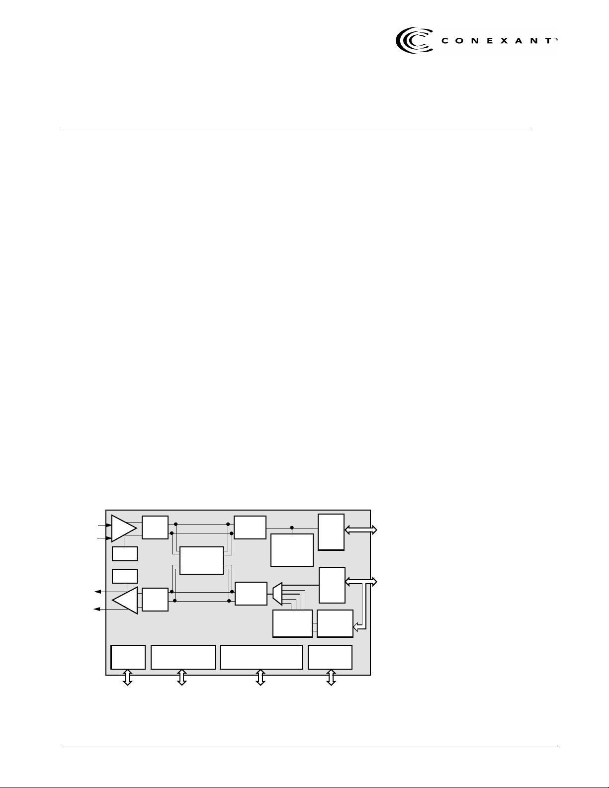
The Bt8370/8375/8376 is a family of single chip transceivers for T1/E1 and Integrated
Service Digital Network (ISDN) primary rate interfaces, operating at 1.544 Mbps or
2.048 Mbps. These devices combine a sophisticated framer, transmit and receive slip
buffers, and an on-chip physical line interface to provide a complete T1/E1 transceiver.
The fully featured Bt8370 and short-haul Bt8375 and Bt8376 devices provide a
programmable clock rate adapter for simplifying system bus interfacing. The adapter
synthesizes standard clock signals from the receive or transmit line rate clocks or from an
external reference.
Operations are controlled through memory-mapped registers accessible via a parallel
microprocessor port. Current ANSI, ETSI, ITU-T, and Bellcore standards are supported for
alarm and error monitoring, signaling supervision (e.g., LAPD/SS7), per-channel trunk
conditioning, and Facility Data Link (FDL) maintenance. A serial Time Division Multiplexed
(TDM) system bus interface allows the backplane Pulse Code Modulation (PCM) data
highway to operate at rates from 1.536 to 8.192 Mbps. Extensive test and diagnostic
functions include a full set of digital and analog loopbacks, PRBS test pattern generation,
BER meter, and forced error insertion.
The physical line interface circuit recovers clock and data from analog signals with +3 to
–43 dB cable attenuation, appropriate for both sho rt (– 18 dB) and lo ng-hau l T 1/E 1
applications. Receive line equalization (EQ) and transmit Line Build Out (LBO) filters are
implemented using Digital Signal Processor (DSP) circuits for reliable performance. Data
and/or clock jitter attenuation can be inserted on either the receive or transmit path. The
transmit section includes precision pulse shaping and amplitude pre-emphasis for cross
connect applications, as well as a set of LBO filters for long-haul Channel Service Unit
(CSU) applications. A complementary driver output is provided to couple 75/100/120 Ω
lines via an external transformer.
Functional Block Diagram
Distinguishing Features
• Single-chip T1/E1 framer with
short/long-haul physical line
interface
• Frames to popular T1/E1 standards:
– T1: SF, ESF, SLC 96, T1DM
– E1: PCM
ISDN primary rate
• On-chip physical line inte rface
compatible with:
– DSX-1/E1 short-haul signals
– DS-1 (T1.403) and ETSI long-haul
signals
• T wo-frame transmit and receive PCM
slip buffers
• Clock rate adapter synthesizes jitter
attenuated system clocks from an
internal or external reference
• Parallel 8-bit microprocessor port
supports Intel or Motorola buses
• Automated Facility Data Link (FDL)
management
• BERT generation and counting
• Two full-duplex HDLC controllers for
data link and LAPD/SS7 signaling
• B8ZS/HDB3/Bit 7 zero suppression
• 80-pin MQFP surface-mount package
• Operates from a single +5 Vdc ±5%
power supply
• Low-power CMOS technology
30, G.704, G.706, G.732
-
Receive
Analog
Transmit
Analog
RX
RPLL
TPLL
TX
JTAG
Test Port
EQ
Pulse
LBO
Control/Status
Registers
Motorola/Intel
Processor Bus
TX or RX
Jitter
Attenuator
ZCS
Decode
T1/E1
Receive
Framer
ZCS
Encode
Overhead
Insertion
Data Link Controllers
DL1 + DL2
External DL3
RX
Slip
Buffer
TX
Slip
Buffer
T1/E1
Transmit
Framer
Clock Rate
Adaptor
CLAD I/ODual-Rail/NRZ/
Receive
System
Bus
Transmit
System
Bus
Applications
• T1/E1 Channel Service Unit/Data
Service Unit (CSU/DSU)
• Digital Access Cross-Connect
Systems (DACS)
• T1/E1 Multiplexer (MUX)
• PBXs and PCM channel bank
• T1/E1 HDSL terminal unit
• ISDN Primary Rate Access (PRA)
Data Sheet N8370DSE
June 30, 1999
Page 2
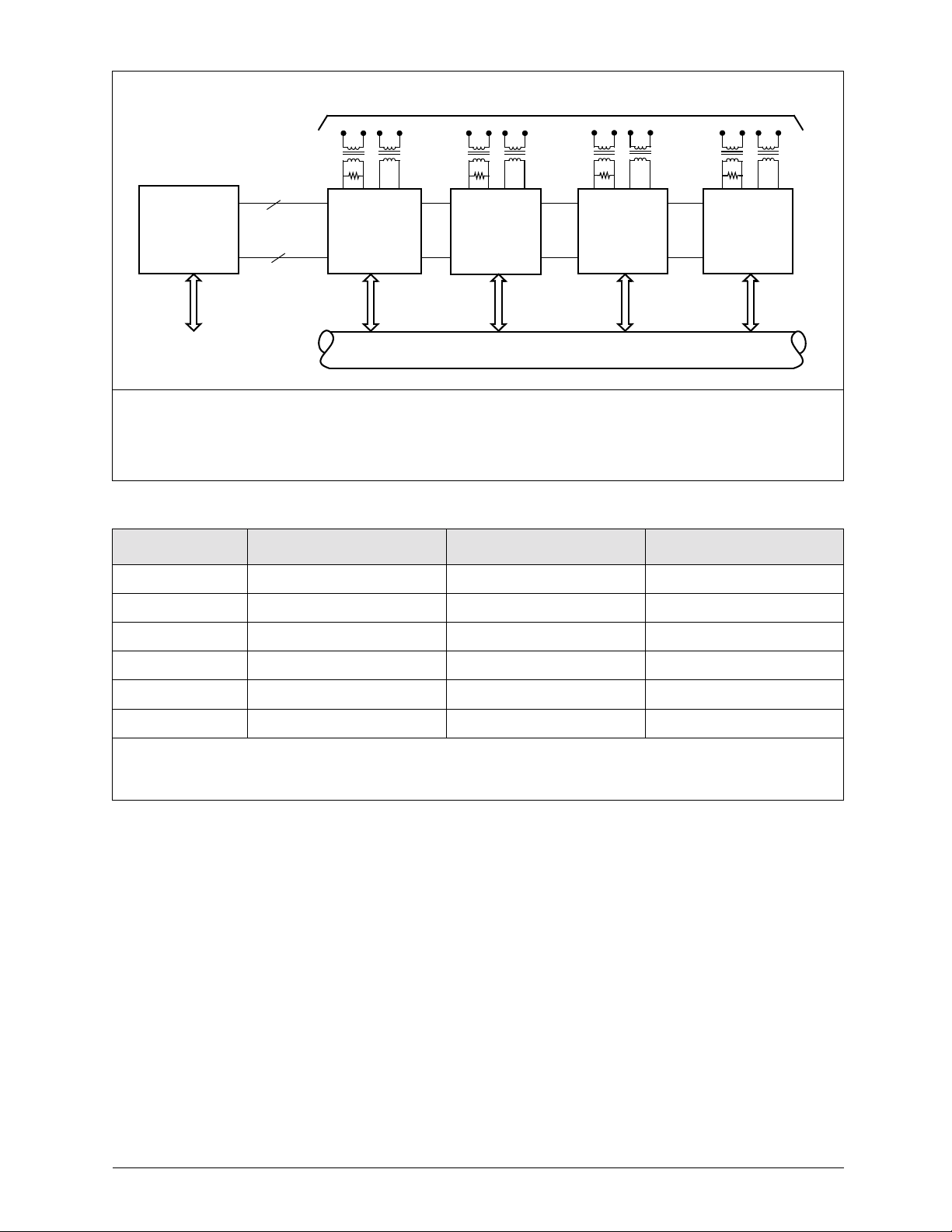
Bt8370EVM—Bt8370 Evaluation Module, Quad T1/E1 ISDN PRI Board
T1 or E1 connection at DSX or CSU levels
Address
Bus
MC68302
Microprocessor
9
Data Bus
8
Bt8370
Bt8370
Bt8370 Bt8370 Bt8370
RS232 User
Interface
Local PCM Highway (128 Channel, 8 MHz)
An evaluation module is available and provides a convenient platform to test and evaluate Bt8370 performance and features. The Bt8370EVM provides up to four T1/E1 transceivers, all necessary line interface circuitry for T1 and E1 connections, and a simple RS232 serial user interface for setting device parameters and displaying status information on
any VT100 compatible terminal. Contact the local sales representative for ordering information and pricing.
Ordering Information
Model Number Package Operating Temperature Reduced Features
Bt8370EPF 80-Pin MQFP –40 to 85 °C none
Bt8370KPF 80-Pin MQFP 0 to 70 °C none
Bt8375EPF 80-Pin MQFP –40 to 85 °C Short-Haul
Bt8375KPF 80-Pin MQFP 0 to 70 °C Short-Haul
Bt8376EPF 80-Pin MQFP –40 to 85 °C Short-Haul, No CLAD output
Bt8376KPF 80-Pin MQFP 0 to 70 °C Short-Haul, No CLAD output
NOTE(S):
(1)
Cost reduced Bt8375 and Bt8376 are pin and register-compatible versions of Bt8370 with reduced features. Contact the local
sales representative for ordering information and pricing.
(1)
Information provided by Conexant Systems, Inc. (Conexant) is believed to be accurate and reliable. However, no responsibility is
assumed by Conexant for its use, nor any infringement of patents or other rights of third parties which may result from its use. No
license is granted by implication or otherwise under any patent rights of Conexant other than for circuitry embodied in Conexant
products. Conexant reserves the right to change circuitry at any time without notice. This document is subject to change without
notice.
Conexant and “What’s Next in Communications Technologies” are trademarks of Conexant Systems, Inc.
Product names or services listed in this publication are for identification purposes only, and may be trademarks or registered
trademarks of their respective companies. All other marks mentioned herein are the property of their respective holders.
© 1999 Conexant Systems, Inc.
Printed in U.S.A.
All Rights Reserved
Reader Response:
To improv e the quality of our publications, w e welcome y our feedback. Please send comments or
suggestions via e-mail to Conexant Reader Response@conexant.com. Sorry, we can't answer your technical
questions at this address. Please contact your local Conexant sales office or applications engineer if you have
technical questions.
N8370DSE
Conexant
Page 3

Table of Contents
List of Figures
List of Tables
1.0 Pin Descriptions
1.1 Pin Assignments
. . . . . . . . . . . . . . . . . . . . . . . . . . . . . . . . . . . . . . . . . . . . . . . . . . . . . . . . . . . . . . . . . . . . . . . . xii
. . . . . . . . . . . . . . . . . . . . . . . . . . . . . . . . . . . . . . . . . . . . . . . . . . . . . . . . . . . . . . . . . . . . . . . . . xv
. . . . . . . . . . . . . . . . . . . . . . . . . . . . . . . . . . . . . . . . . . . . . . . . . . . . . . . . . . . . . . . . 1-1
2.0 Circuit Description
2.1 Bt8370/8375/8376 Block Diagrams
2.2 Receive Line Interface Unit
2.2.1 Data Recovery
2.2.1.1 Automatic Gain Control
2.2.1.2 Variable Gain Amplifier
2.2.1.3 Adaptive Equalizer
2.2.1.4 Data Slicer
2.2.2 Clock Recovery
2.2.2.1 Phase Locked Loop
2.3 Jitter Attenuator
2.3.1 Elastic Store
2.4 Receiver
2.4.1 ZCS Decoder
2.4.2 In-Band Loopback Code Detection
2.4.3 Error Counters
2.4.4 Error Monitor
. . . . . . . . . . . . . . . . . . . . . . . . . . . . . . . . . . . . . . . . . . . . . . . . . . . . . . . . . . . . . . . . . 2-14
2.4.3.1 Frame Bit Error Counter
2.4.3.2 CRC Error Counter
2.4.3.3 LCV Error Counter
2.4.3.4 FEBE Counter
. . . . . . . . . . . . . . . . . . . . . . . . . . . . . . . . . . . . . . . . . . . . . . . . . . . . . . . . . . . . 1-1
. . . . . . . . . . . . . . . . . . . . . . . . . . . . . . . . . . . . . . . . . . . . . . . . . . . . . . . . . . . . . . 2-1
. . . . . . . . . . . . . . . . . . . . . . . . . . . . . . . . . . . . . . . . . . . . . . 2-1
. . . . . . . . . . . . . . . . . . . . . . . . . . . . . . . . . . . . . . . . . . . . . . . . . . . . 2-5
. . . . . . . . . . . . . . . . . . . . . . . . . . . . . . . . . . . . . . . . . . . . . . . . . . . . . . . . 2-7
. . . . . . . . . . . . . . . . . . . . . . . . . . . . . . . . . . . . . . . . . 2-7
. . . . . . . . . . . . . . . . . . . . . . . . . . . . . . . . . . . . . . . . . 2-7
. . . . . . . . . . . . . . . . . . . . . . . . . . . . . . . . . . . . . . . . . . . . . 2-7
. . . . . . . . . . . . . . . . . . . . . . . . . . . . . . . . . . . . . . . . . . . . . . . . . . 2-7
. . . . . . . . . . . . . . . . . . . . . . . . . . . . . . . . . . . . . . . . . . . . . . . . . . . . . . . 2-8
. . . . . . . . . . . . . . . . . . . . . . . . . . . . . . . . . . . . . . . . . . . . 2-8
. . . . . . . . . . . . . . . . . . . . . . . . . . . . . . . . . . . . . . . . . . . . . . . . . . . . . . . . . . . . 2-9
. . . . . . . . . . . . . . . . . . . . . . . . . . . . . . . . . . . . . . . . . . . . . . . . . . . . . . . . . 2-10
. . . . . . . . . . . . . . . . . . . . . . . . . . . . . . . . . . . . . . . . . . . . . . . . . . . . . . . . 2-15
. . . . . . . . . . . . . . . . . . . . . . . . . . . . . . . . . . . . . . . . 2-15
. . . . . . . . . . . . . . . . . . . . . . . . . . . . . . . . . . . . . . . . . . . . . . . . . . . . . . . 2-16
. . . . . . . . . . . . . . . . . . . . . . . . . . . . . . . . . . . . . . . . 2-16
. . . . . . . . . . . . . . . . . . . . . . . . . . . . . . . . . . . . . . . . . . . 2-16
. . . . . . . . . . . . . . . . . . . . . . . . . . . . . . . . . . . . . . . . . . . . 2-16
. . . . . . . . . . . . . . . . . . . . . . . . . . . . . . . . . . . . . . . . . . . . . . . 2-16
. . . . . . . . . . . . . . . . . . . . . . . . . . . . . . . . . . . . . . . . . . . . . . . . . . . . . . . . 2-17
N8370DSE
Conexant
iii
Page 4

Table of Contents
Bt8370/8375/8376
2.4.5 Alarm Monitor
2.4.5.1 Loss of Frame
2.4.5.2 Loss of Signal
2.4.5.3 Analog Loss of Signal
2.4.5.4 Alarm Indication Signal
2.4.5.5 Yellow Alarm
2.4.5.6 Multiframe YEL
2.4.5.7 Severely Errored Frame
2.4.5.8 Change of Frame Alignment
2.4.5.9 Receive Multiframe AIS
2.4.6 Test Pattern Receiver
2.4.7 Receive Framing
2.4.8 External Receive Data Link
2.4.9 Sa-Byte Receive Buffers
2.4.10 Receive Data Link
2.4.10.1 Data Link Controllers
2.4.10.2 RBOP Receiver
2.5 Receive System Bus
2.5.1 Timebase
2.5.2 Slip Buffer
2.5.3 Signaling Buffer
2.5.4 Signaling Stack
2.5.5 Embedded Framing
. . . . . . . . . . . . . . . . . . . . . . . . . . . . . . . . . . . . . . . . . . . . . . . . . . . . . . . 2-18
. . . . . . . . . . . . . . . . . . . . . . . . . . . . . . . . . . . . . . . . . . . . . . . 2-18
. . . . . . . . . . . . . . . . . . . . . . . . . . . . . . . . . . . . . . . . . . . . . . . 2-18
. . . . . . . . . . . . . . . . . . . . . . . . . . . . . . . . . . . . . . . . . 2-19
. . . . . . . . . . . . . . . . . . . . . . . . . . . . . . . . . . . . . . . . 2-19
. . . . . . . . . . . . . . . . . . . . . . . . . . . . . . . . . . . . . . . . . . . . . . . . 2-19
. . . . . . . . . . . . . . . . . . . . . . . . . . . . . . . . . . . . . . . . . . . . . . 2-19
. . . . . . . . . . . . . . . . . . . . . . . . . . . . . . . . . . . . . . . . 2-19
. . . . . . . . . . . . . . . . . . . . . . . . . . . . . . . . . . . . . . . . 2-19
. . . . . . . . . . . . . . . . . . . . . . . . . . . . . . . . . . . . . . . . . . . . . . . . . . 2-20
. . . . . . . . . . . . . . . . . . . . . . . . . . . . . . . . . . . . . . . . . . . . . . . . . . . . . . 2-21
. . . . . . . . . . . . . . . . . . . . . . . . . . . . . . . . . . . . . . . . . . . . . . 2-26
. . . . . . . . . . . . . . . . . . . . . . . . . . . . . . . . . . . . . . . . . . . . . . . . 2-26
. . . . . . . . . . . . . . . . . . . . . . . . . . . . . . . . . . . . . . . . . . . . . . . . . . . . . 2-26
. . . . . . . . . . . . . . . . . . . . . . . . . . . . . . . . . . . . . . . . . . 2-27
. . . . . . . . . . . . . . . . . . . . . . . . . . . . . . . . . . . . . . . . . . . . . . 2-31
. . . . . . . . . . . . . . . . . . . . . . . . . . . . . . . . . . . . . . . . . . . . . . . . . . . . . . . . 2-32
. . . . . . . . . . . . . . . . . . . . . . . . . . . . . . . . . . . . . . . . . . . . . . . . . . . . . . . . . . . 2-35
. . . . . . . . . . . . . . . . . . . . . . . . . . . . . . . . . . . . . . . . . . . . . . . . . . . . . . . . . . 2-36
. . . . . . . . . . . . . . . . . . . . . . . . . . . . . . . . . . . . . . . . . . . . . . . . . . . . . . 2-37
. . . . . . . . . . . . . . . . . . . . . . . . . . . . . . . . . . . . . . . . . . . . . . . . . . . . . . 2-38
. . . . . . . . . . . . . . . . . . . . . . . . . . . . . . . . . . . . . . . . . . . . . . . . . . . 2-38
Fully Integrated T1/E1 Framer and Line Interface
. . . . . . . . . . . . . . . . . . . . . . . . . . . . . . . . . . . . . 2-19
2.6 Clock Rate Adapter
2.6.1 Configuring the CLAD Registers
2.7 Transmit System Bus
2.7.1 Timebase
2.7.2 Slip Buffer
2.7.3 Signaling Buffer
2.7.4 Transmit Framing
2.7.5 Embedded Framing
2.8 Transmitter
2.8.1 External Transmit Data Link
2.8.2 Transmit Data Links
2.8.3 Sa-Byte Overwrite Buffer
2.8.4 Overhead Pattern Generator
. . . . . . . . . . . . . . . . . . . . . . . . . . . . . . . . . . . . . . . . . . . . . . . . . . . . . . . . . . . . . . . 2-53
2.8.2.1 Data Link Controllers
2.8.2.2 PRM Generator
2.8.4.1 Framing Pattern Generation
2.8.4.2 Alarm Generator
2.8.4.3 CRC Generation
2.8.4.4 Far-End Block Error Generation
. . . . . . . . . . . . . . . . . . . . . . . . . . . . . . . . . . . . . . . . . . . . . . . . . . . . . . . . . 2-39
. . . . . . . . . . . . . . . . . . . . . . . . . . . . . . . . . . . . . . . . . . . . . . . . . . . . . . . . 2-46
. . . . . . . . . . . . . . . . . . . . . . . . . . . . . . . . . . . . . . . . . . . . . . . . . . . . . . . . . . . 2-48
. . . . . . . . . . . . . . . . . . . . . . . . . . . . . . . . . . . . . . . . . . . . . . . . . . . . . . . . . . 2-48
. . . . . . . . . . . . . . . . . . . . . . . . . . . . . . . . . . . . . . . . . . 2-43
. . . . . . . . . . . . . . . . . . . . . . . . . . . . . . . . . . . . . . . . . . . . . . . . . . . . . . 2-49
. . . . . . . . . . . . . . . . . . . . . . . . . . . . . . . . . . . . . . . . . . . . . . . . . . . . . 2-50
. . . . . . . . . . . . . . . . . . . . . . . . . . . . . . . . . . . . . . . . . . . . . . . . . . . 2-52
. . . . . . . . . . . . . . . . . . . . . . . . . . . . . . . . . . . . . . . . . . . . . 2-54
. . . . . . . . . . . . . . . . . . . . . . . . . . . . . . . . . . . . . . . . . . . . . . . . . . . 2-54
. . . . . . . . . . . . . . . . . . . . . . . . . . . . . . . . . . . . . . . . . . 2-54
. . . . . . . . . . . . . . . . . . . . . . . . . . . . . . . . . . . . . . . . . . . . . . 2-59
. . . . . . . . . . . . . . . . . . . . . . . . . . . . . . . . . . . . . . . . . . . . . . . 2-59
. . . . . . . . . . . . . . . . . . . . . . . . . . . . . . . . . . . . . . . . . . . . . 2-60
. . . . . . . . . . . . . . . . . . . . . . . . . . . . . . . . . . . . . 2-60
. . . . . . . . . . . . . . . . . . . . . . . . . . . . . . . . . . . . . . . . . . . . . 2-60
. . . . . . . . . . . . . . . . . . . . . . . . . . . . . . . . . . . . . . . . . . . . . 2-63
. . . . . . . . . . . . . . . . . . . . . . . . . . . . . . . . . . 2-63
iv
Conexant
N8370DSE
Page 5

Bt8370/8375/8376
Table of Contents
Fully Integrated T1/E1 Framer and Line Interface
2.8.5 Test Pattern Generator
2.8.6 Transmit Error Insertion
2.8.7 In-Band Loopback Code Generator
2.8.8 ZCS Encoder
2.9 Transmit Line Interface Unit
2.9.1 Pulse Shape
2.9.2 Transmit Phase Lock Loop
2.9.2.1 Clock Reference
2.9.2.2 Output Jitter
2.9.3 Line Build Out
2.9.4 Line Driver
2.9.4.1 Termination Impedance
2.9.4.2 Return Loss
2.9.4.3 Output Enable
2.9.5 Pulse Imbalance
2.10 Microprocessor Interface
2.10.1 Address/Data Bus
2.10.2 Bus Control Signals
2.10.3 Interrupt Requests
2.10.4 Device Reset
2.10.4.1 Power-On Reset (POR)
2.10.4.2 Hardware Reset
2.10.4.3 Software Reset
. . . . . . . . . . . . . . . . . . . . . . . . . . . . . . . . . . . . . . . . . . . . . . . . . . . . . . . . 2-65
. . . . . . . . . . . . . . . . . . . . . . . . . . . . . . . . . . . . . . . . . . . . . . . . . . . . . . . . . 2-70
. . . . . . . . . . . . . . . . . . . . . . . . . . . . . . . . . . . . . . . . . . . . . . . . . . . . . . . 2-77
. . . . . . . . . . . . . . . . . . . . . . . . . . . . . . . . . . . . . . . . . . . . . . . . . . . . . . . . . . 2-80
. . . . . . . . . . . . . . . . . . . . . . . . . . . . . . . . . . . . . . . . . . . . . . . . . . . . . . . . 2-85
. . . . . . . . . . . . . . . . . . . . . . . . . . . . . . . . . . . . . . . . . . . . . . . . . 2-63
. . . . . . . . . . . . . . . . . . . . . . . . . . . . . . . . . . . . . . . . . . . . . . . . . . 2-68
. . . . . . . . . . . . . . . . . . . . . . . . . . . . . . . . . . . . . . . . . . . . . . . . . . . . . . 2-82
. . . . . . . . . . . . . . . . . . . . . . . . . . . . . . . . . . . . . . . . . . . . . . . . . . . . 2-83
. . . . . . . . . . . . . . . . . . . . . . . . . . . . . . . . . . . . . . . . . . . . . . . . . . . . . 2-84
. . . . . . . . . . . . . . . . . . . . . . . . . . . . . . . . . . . . . . . . . . . . . . . . . . . 2-84
. . . . . . . . . . . . . . . . . . . . . . . . . . . . . . . . . . . . . . . . . . . . . . . . . . . . 2-84
. . . . . . . . . . . . . . . . . . . . . . . . . . . . . . . . . . . . . . . . . . . . . . . . 2-64
. . . . . . . . . . . . . . . . . . . . . . . . . . . . . . . . . . . . . . . . 2-65
. . . . . . . . . . . . . . . . . . . . . . . . . . . . . . . . . . . . . . . . . . . . . . 2-76
. . . . . . . . . . . . . . . . . . . . . . . . . . . . . . . . . . . . . . . . . . . . . 2-76
. . . . . . . . . . . . . . . . . . . . . . . . . . . . . . . . . . . . . . . . . . . . . . . . 2-77
. . . . . . . . . . . . . . . . . . . . . . . . . . . . . . . . . . . . . . . . 2-80
. . . . . . . . . . . . . . . . . . . . . . . . . . . . . . . . . . . . . . . . . . . . . . . . 2-81
. . . . . . . . . . . . . . . . . . . . . . . . . . . . . . . . . . . . . . . . . . . . . . . 2-82
. . . . . . . . . . . . . . . . . . . . . . . . . . . . . . . . . . . . . . . . 2-85
. . . . . . . . . . . . . . . . . . . . . . . . . . . . . . . . . . . . . . . . . . . . . 2-85
. . . . . . . . . . . . . . . . . . . . . . . . . . . . . . . . . . . . . . . . . . . . . . 2-85
2.11 Loopbacks
2.11.1 Remote Line Loopback
2.11.2 Remote Payload Loopback
2.11.3 Remote Per-Channel Loopbacks
2.11.4 Local Analog Loopback
2.11.5 Local Framer Loopback
2.11.6 Local Per-Channel Loopback
2.12 Joint Test Access Group
2.12.1 Instructions
2.12.2 Device Identification Register
. . . . . . . . . . . . . . . . . . . . . . . . . . . . . . . . . . . . . . . . . . . . . . . . . . . . . . . . . . . . . . . . 2-86
. . . . . . . . . . . . . . . . . . . . . . . . . . . . . . . . . . . . . . . . . . . . . . . . . . . . . 2-88
. . . . . . . . . . . . . . . . . . . . . . . . . . . . . . . . . . . . . . . . . . . . . . . . . . . . . . . . . 2-88
. . . . . . . . . . . . . . . . . . . . . . . . . . . . . . . . . . . . . . . . . . . . . . . . . 2-86
. . . . . . . . . . . . . . . . . . . . . . . . . . . . . . . . . . . . . . . . . . . . . . 2-86
. . . . . . . . . . . . . . . . . . . . . . . . . . . . . . . . . . . . . . . . . . 2-86
. . . . . . . . . . . . . . . . . . . . . . . . . . . . . . . . . . . . . . . . . . . . . . . . 2-87
. . . . . . . . . . . . . . . . . . . . . . . . . . . . . . . . . . . . . . . . . . . . . . . . 2-87
. . . . . . . . . . . . . . . . . . . . . . . . . . . . . . . . . . . . . . . . . . . . . 2-87
. . . . . . . . . . . . . . . . . . . . . . . . . . . . . . . . . . . . . . . . . . . . 2-89
N8370DSE
Conexant
v
Page 6

Table of Contents
Bt8370/8375/8376
3.0 Registers
3.1 Address Map
3.2 Global Control and Status Registers
3.3 Interrupt Control Register
3.4 Interrupt Status Registers
Fully Integrated T1/E1 Framer and Line Interface
. . . . . . . . . . . . . . . . . . . . . . . . . . . . . . . . . . . . . . . . . . . . . . . . . . . . . . . . . . . . . . . . . . . . . . 3-1
. . . . . . . . . . . . . . . . . . . . . . . . . . . . . . . . . . . . . . . . . . . . . . . . . . . . . . . . . . . . . . . 3-1
. . . . . . . . . . . . . . . . . . . . . . . . . . . . . . . . . . . . . . . . . . . . . 3-9
000—Device Identification (DID)
001—Primary Control Register (CR0)
002—Jitter Attenuator Configuration (JAT_CR)
. . . . . . . . . . . . . . . . . . . . . . . . . . . . . . . . . . . . . . . . . . 3-9
. . . . . . . . . . . . . . . . . . . . . . . . . . . . . . . . . . . . . . . 3-9
. . . . . . . . . . . . . . . . . . . . . . . . . . . . . . . 3-11
. . . . . . . . . . . . . . . . . . . . . . . . . . . . . . . . . . . . . . . . . . . . . . . . . . . . 3-13
003—Interrupt Request Register (IRR)
. . . . . . . . . . . . . . . . . . . . . . . . . . . . . . . . . . . . . 3-13
. . . . . . . . . . . . . . . . . . . . . . . . . . . . . . . . . . . . . . . . . . . . . . . . . . . . 3-15
004—Alarm 1 Interrupt Status (ISR7)
005—Alarm 2 Interrupt Status (ISR6)
006—Error Interrupt Status (ISR5)
007—Counter Overflow Interrupt Status (ISR4)
008—Timer Interrupt Status (ISR3)
009—Data Link 1 Interrupt Status (ISR2)
00A—Data Link 2 Interrupt Status (ISR1)
00B—Pattern Interrupt Status (ISR0)
. . . . . . . . . . . . . . . . . . . . . . . . . . . . . . . . . . . . . . 3-16
. . . . . . . . . . . . . . . . . . . . . . . . . . . . . . . . . . . . . . 3-17
. . . . . . . . . . . . . . . . . . . . . . . . . . . . . . . . . . . . . . . . 3-18
. . . . . . . . . . . . . . . . . . . . . . . . . . . . . . 3-19
. . . . . . . . . . . . . . . . . . . . . . . . . . . . . . . . . . . . . . . 3-19
. . . . . . . . . . . . . . . . . . . . . . . . . . . . . . . . . . . 3-20
. . . . . . . . . . . . . . . . . . . . . . . . . . . . . . . . . . . 3-21
. . . . . . . . . . . . . . . . . . . . . . . . . . . . . . . . . . . . . . 3-22
3.5 Interrupt Enable Registers
00C—Alarm 1 Interrupt Enable Register (IER7)
00D—Alarm 2 Interrupt Enable Register (IER6)
00E—Error Interrupt Enable Register (IER5)
00F—Count Overflow Interrupt Enable Register (IER4)
010—Timer Interrupt Enable Register (IER3)
011—Data Link 1 Interrupt Enable Register (IER2)
012—Data Link 2 Interrupt Enable Register (IER1)
013—Pattern Interrupt Enable Register (IER0)
3.6 Primary Control and Status Registers
014—Loopback Configuration Register (LOOP)
015—External Data Link Time Slot (DL3_TS)
016—External Data Link Bit (DL3_BIT)
017—Offline Framer Status (FSTAT)
018—Programmable Input/Output (PIO)
019—Programmable Output Enable (POE)
01A—Clock Input Mux (CMUX)
01B—Test Mux Configuration (TMUX)
01C—Test Configuration (TEST)
. . . . . . . . . . . . . . . . . . . . . . . . . . . . . . . . . . . . . . . . . . . . . . . . . . . 3-23
. . . . . . . . . . . . . . . . . . . . . . . . . . . . . . . 3-23
. . . . . . . . . . . . . . . . . . . . . . . . . . . . . . . 3-23
. . . . . . . . . . . . . . . . . . . . . . . . . . . . . . . . . 3-24
. . . . . . . . . . . . . . . . . . . . . . . . . 3-24
. . . . . . . . . . . . . . . . . . . . . . . . . . . . . . . . 3-25
. . . . . . . . . . . . . . . . . . . . . . . . . . . . 3-25
. . . . . . . . . . . . . . . . . . . . . . . . . . . . 3-26
. . . . . . . . . . . . . . . . . . . . . . . . . . . . . . . 3-26
. . . . . . . . . . . . . . . . . . . . . . . . . . . . . . . . . . . . . . . . . . . 3-27
. . . . . . . . . . . . . . . . . . . . . . . . . . . . . . 3-27
. . . . . . . . . . . . . . . . . . . . . . . . . . . . . . . . 3-28
. . . . . . . . . . . . . . . . . . . . . . . . . . . . . . . . . . . . . 3-29
. . . . . . . . . . . . . . . . . . . . . . . . . . . . . . . . . . . . . . . 3-29
. . . . . . . . . . . . . . . . . . . . . . . . . . . . . . . . . . . . 3-32
. . . . . . . . . . . . . . . . . . . . . . . . . . . . . . . . . . 3-35
. . . . . . . . . . . . . . . . . . . . . . . . . . . . . . . . . . . . . . . . . . 3-36
. . . . . . . . . . . . . . . . . . . . . . . . . . . . . . . . . . . . . 3-37
. . . . . . . . . . . . . . . . . . . . . . . . . . . . . . . . . . . . . . . . . . 3-37
vi
Conexant
N8370DSE
Page 7

Bt8370/8375/8376
Table of Contents
Fully Integrated T1/E1 Framer and Line Interface
3.7 Receive LIU Registers
020—LIU Configuration (LIU_CR)
021—Receive LIU Status (RSTAT)
022—Receive LIU Configuration (RLIU_CR)
023—RPLL Low Pass Filter (LPF)
024—Variable Gain Amplifier Maximum (VGA_MAX)
025—Equalizer Coefficient Data Register (EQ_DAT)
026—Equalizer Coefficient Table Pointer (EQ_PTR)
027—Data Slicer Threshold (DSLICE)
028—Equalizer Output Levels
029—Variable Gain Amplifier Status
02A—Pre_Equalizer (PRE_EQ)
030–037—LMS Adjusted Equalizer Coefficient Status (COEFF)
038–03C—Equalizer Gain Thresholds (GAIN)
3.8 Receiver Registers
040—Receiver Configuration (RCR0)
041—Receive Test Pattern Configuration (RPATT)
042—Receive Loopback Code Detector Configuration (RLB)
043—Loopback Activate Code Pattern (LBA)
044—Loopback Deactivate Code Pattern (LBD)
045—Receive Alarm Signal Configuration (RALM)
046—Alarm/Error/Counter Latch Configuration (LATCH)
047—Alarm 1 Status (ALM1)
048—Alarm 2 Status (ALM2)
049—Alarm 3 Status (ALM3)
. . . . . . . . . . . . . . . . . . . . . . . . . . . . . . . . . . . . . . . . . . . . . . . . . . . . . . . 3-38
. . . . . . . . . . . . . . . . . . . . . . . . . . . . . . . . . . . . . . . . . . . . . . . . . . . . . . . . . 3-47
. . . . . . . . . . . . . . . . . . . . . . . . . . . . . . . . . . . . . . . . 3-39
. . . . . . . . . . . . . . . . . . . . . . . . . . . . . . . . . . . . . . . . 3-40
. . . . . . . . . . . . . . . . . . . . . . . . . . . . . . . . . 3-41
. . . . . . . . . . . . . . . . . . . . . . . . . . . . . . . . . . . . . . . . . 3-42
. . . . . . . . . . . . . . . . . . . . . . . . . . . 3-42
. . . . . . . . . . . . . . . . . . . . . . . . . . . . 3-43
. . . . . . . . . . . . . . . . . . . . . . . . . . . . 3-43
. . . . . . . . . . . . . . . . . . . . . . . . . . . . . . . . . . . . . . 3-43
. . . . . . . . . . . . . . . . . . . . . . . . . . . . . . . . . . . . . . . . . . . . 3-44
. . . . . . . . . . . . . . . . . . . . . . . . . . . . . . . . . . . . . . . 3-45
. . . . . . . . . . . . . . . . . . . . . . . . . . . . . . . . . . . . . . . . . . . 3-46
. . . . . . . . . . . . . . . . . . . 3-46
. . . . . . . . . . . . . . . . . . . . . . . . . . . . . . . . 3-46
. . . . . . . . . . . . . . . . . . . . . . . . . . . . . . . . . . . . . . 3-47
. . . . . . . . . . . . . . . . . . . . . . . . . . . . . 3-48
. . . . . . . . . . . . . . . . . . . . . 3-50
. . . . . . . . . . . . . . . . . . . . . . . . . . . . . . . . . 3-50
. . . . . . . . . . . . . . . . . . . . . . . . . . . . . . . 3-51
. . . . . . . . . . . . . . . . . . . . . . . . . . . . 3-51
. . . . . . . . . . . . . . . . . . . . . . . . 3-52
. . . . . . . . . . . . . . . . . . . . . . . . . . . . . . . . . . . . . . . . . . . . 3-53
. . . . . . . . . . . . . . . . . . . . . . . . . . . . . . . . . . . . . . . . . . . . 3-56
. . . . . . . . . . . . . . . . . . . . . . . . . . . . . . . . . . . . . . . . . . . . 3-57
3.9 Performance Monitoring Registers
050—Framing Bit Error Counter LSB (FERR)
051—Framing Bit Error Counter MSB (FERR)
052—CRC Error Counter LSB (CERR)
053—CRC Error Counter MSB (CERR)
054—Line Code Violation Counter LSB (LCV)
055—Line Code Violation Counter MSB (LCV)
056—Far End Block Error Counter LSB (FEBE)
057—Far End Block Error Counter MSB (FEBE)
058—PRBS Bit Error Counter LSB (BERR)
059—PRBS Bit Error Counter MSB (BERR)
05A—SEF/LOF/COFA Alarm Counter (AERR)
3.10 Receive Sa-Byte Buffers
05B—Receive Sa4 Byte Buffer (RSA4)
05C—Receive Sa5 Byte Buffer (RSA5)
05D—Receive Sa6 Byte Buffer (RSA6)
05E—Receive Sa7 Byte Buffer (RSA7)
05F—Receive Sa8 Byte Buffer (RSA8)
. . . . . . . . . . . . . . . . . . . . . . . . . . . . . . . . . . . . . . . . . . . . . . . . . . . . . 3-61
. . . . . . . . . . . . . . . . . . . . . . . . . . . . . . . . . . . . . . . . . . . . . 3-58
. . . . . . . . . . . . . . . . . . . . . . . . . . . . . . . . 3-58
. . . . . . . . . . . . . . . . . . . . . . . . . . . . . . . . 3-58
. . . . . . . . . . . . . . . . . . . . . . . . . . . . . . . . . . . . . . 3-58
. . . . . . . . . . . . . . . . . . . . . . . . . . . . . . . . . . . . . 3-59
. . . . . . . . . . . . . . . . . . . . . . . . . . . . . . . . 3-59
. . . . . . . . . . . . . . . . . . . . . . . . . . . . . . . 3-59
. . . . . . . . . . . . . . . . . . . . . . . . . . . . . . . 3-59
. . . . . . . . . . . . . . . . . . . . . . . . . . . . . . . 3-59
. . . . . . . . . . . . . . . . . . . . . . . . . . . . . . . . . . 3-60
. . . . . . . . . . . . . . . . . . . . . . . . . . . . . . . . . 3-60
. . . . . . . . . . . . . . . . . . . . . . . . . . . . . . . . . 3-60
. . . . . . . . . . . . . . . . . . . . . . . . . . . . . . . . . . . . . 3-61
. . . . . . . . . . . . . . . . . . . . . . . . . . . . . . . . . . . . . 3-61
. . . . . . . . . . . . . . . . . . . . . . . . . . . . . . . . . . . . . 3-62
. . . . . . . . . . . . . . . . . . . . . . . . . . . . . . . . . . . . . 3-62
. . . . . . . . . . . . . . . . . . . . . . . . . . . . . . . . . . . . . 3-63
N8370DSE
Conexant
vii
Page 8

Table of Contents
Bt8370/8375/8376
3.11 Transmit LIU Registers
060–067—Transmit Pulse Shape Configuration (SHAPE)
068—Transmit LIU Configuration (TLIU_CR)
3.12 Transmitter Registers
070—Transmit Framer Configuration (TCR0)
071—Transmitter Configuration (TCR1)
072—Transmit Frame Format (TFRM)
073—Transmit Error Insert (TERROR)
074—Transmit Manual Sa-Byte/FEBE Configuration (TMAN)
075—Transmit Alarm Signal Configuration (TALM)
076—Transmit Test Pattern Configuration (TPATT)
077—Transmit Inband Loopback Code Configuration (TLB)
078—Transmit Inband Loopback Code Pattern (LBP)
3.13 Transmit Sa-Byte Buffers
07B—Transmit Sa4 Byte Buffer (TSA4)
07C—Transmit Sa5 Byte Buffer (TSA5)
07D—Transmit Sa6 Byte Buffer (TSA6)
07E—Transmit Sa7 Byte Buffer (TSA7)
07F—Transmit Sa8 Byte Buffer (TSA8)
. . . . . . . . . . . . . . . . . . . . . . . . . . . . . . . . . . . . . . . . . . . . . . . . . . . . . . 3-64
. . . . . . . . . . . . . . . . . . . . . . . . . . . . . . . . . . . . . . . . . . . . . . . . . . . . . . . 3-67
. . . . . . . . . . . . . . . . . . . . . . . . . . . . . . . . . . . . . . . . . . . . . . . . . . . . . 3-80
Fully Integrated T1/E1 Framer and Line Interface
. . . . . . . . . . . . . . . . . . . . . . . 3-64
. . . . . . . . . . . . . . . . . . . . . . . . . . . . . . . . 3-64
. . . . . . . . . . . . . . . . . . . . . . . . . . . . . . . . 3-67
. . . . . . . . . . . . . . . . . . . . . . . . . . . . . . . . . . . . 3-71
. . . . . . . . . . . . . . . . . . . . . . . . . . . . . . . . . . . . . . 3-73
. . . . . . . . . . . . . . . . . . . . . . . . . . . . . . . . . . . . . 3-74
. . . . . . . . . . . . . . . . . . . . . 3-75
. . . . . . . . . . . . . . . . . . . . . . . . . . . . 3-76
. . . . . . . . . . . . . . . . . . . . . . . . . . . . 3-77
. . . . . . . . . . . . . . . . . . . . . . 3-79
. . . . . . . . . . . . . . . . . . . . . . . . . . 3-79
. . . . . . . . . . . . . . . . . . . . . . . . . . . . . . . . . . . . . 3-80
. . . . . . . . . . . . . . . . . . . . . . . . . . . . . . . . . . . . . 3-80
. . . . . . . . . . . . . . . . . . . . . . . . . . . . . . . . . . . . . 3-81
. . . . . . . . . . . . . . . . . . . . . . . . . . . . . . . . . . . . . 3-81
. . . . . . . . . . . . . . . . . . . . . . . . . . . . . . . . . . . . . 3-82
3.14 Clock Rate Adapter Registers
090—Clock Rate Adapter Configuration (CLAD_CR)
091—CLAD Frequency Select (CSEL)
092—CLAD Phase Detector Scale Factor (CPHASE)
093—CLAD Test (CTEST)
3.15 Bit-Oriented Protocol Registers
0A0—Bit Oriented Protocol Transceiver (BOP)
0A1—Transmit BOP Codeword (TBOP)
0A2—Receive BOP Codeword (RBOP)
0A3—BOP Status (BOP_STAT)
3.16 Data Link Registers
0A4—DL1 Time Slot Enable (DL1_TS)
0A5—DL1 Bit Enable (DL1_BIT)
0A6—DL1 Control (DL1_CTL)
0A7—RDL #1 FIFO Fill Control (RDL1_FFC)
0A8—Receive Data Link FIFO #1 (RDL1)
0A9—RDL #1 Status (RDL1_STAT)
0AA—Performance Report Message (PRM)
0AB—TDL #1 FIFO Empty Control (TDL1_FEC)
0AC—TDL #1 End Of Message Control (TDL1_EOM)
0AD—Transmit Data Link FIFO #1 (TDL1)
0AE—TDL #1 Status (TDL1_STAT)
0AF—DL2 Time Slot Enable (DL2_TS)
. . . . . . . . . . . . . . . . . . . . . . . . . . . . . . . . . . . . . . . . . . . . . . . . . . . . . . . . . 3-91
. . . . . . . . . . . . . . . . . . . . . . . . . . . . . . . . . . . . . . . . . . . . . . . . . 3-83
. . . . . . . . . . . . . . . . . . . . . . . . . . . 3-83
. . . . . . . . . . . . . . . . . . . . . . . . . . . . . . . . . . . . . . 3-84
. . . . . . . . . . . . . . . . . . . . . . . . . . . 3-85
. . . . . . . . . . . . . . . . . . . . . . . . . . . . . . . . . . . . . . . . . . . . . . . 3-86
. . . . . . . . . . . . . . . . . . . . . . . . . . . . . . . . . . . . . . . . . . . . . . . . 3-87
. . . . . . . . . . . . . . . . . . . . . . . . . . . . . . . 3-87
. . . . . . . . . . . . . . . . . . . . . . . . . . . . . . . . . . . . . 3-89
. . . . . . . . . . . . . . . . . . . . . . . . . . . . . . . . . . . . . 3-90
. . . . . . . . . . . . . . . . . . . . . . . . . . . . . . . . . . . . . . . . . . . 3-90
. . . . . . . . . . . . . . . . . . . . . . . . . . . . . . . . . . . . . 3-91
. . . . . . . . . . . . . . . . . . . . . . . . . . . . . . . . . . . . . . . . . . 3-92
. . . . . . . . . . . . . . . . . . . . . . . . . . . . . . . . . . . . . . . . . . . 3-92
. . . . . . . . . . . . . . . . . . . . . . . . . . . . . . . . . 3-95
. . . . . . . . . . . . . . . . . . . . . . . . . . . . . . . . . . . . 3-96
. . . . . . . . . . . . . . . . . . . . . . . . . . . . . . . . . . . . . . . 3-97
. . . . . . . . . . . . . . . . . . . . . . . . . . . . . . . . . 3-98
. . . . . . . . . . . . . . . . . . . . . . . . . . . . . . . 3-99
. . . . . . . . . . . . . . . . . . . . . . . . . . 3-100
. . . . . . . . . . . . . . . . . . . . . . . . . . . . . . . . . . 3-100
. . . . . . . . . . . . . . . . . . . . . . . . . . . . . . . . . . . . . . . 3-100
. . . . . . . . . . . . . . . . . . . . . . . . . . . . . . . . . . . . 3-101
viii
Conexant
N8370DSE
Page 9

Bt8370/8375/8376
Table of Contents
Fully Integrated T1/E1 Framer and Line Interface
0B0—DL2 Bit Enable (DL2_BIT)
0B1—DL2 Control (DL2_CTL)
0B2—RDL #2 FIFO Fill Control (RDL2_FFC)
0B3—Receive Data Link FIFO #2 (RDL2)
0B4—RDL #2 Status (RDL2_STAT)
0B6—TDL #2 FIFO Empty Control (TDL2_FEC)
0B7—TDL #2 End Of Message Control (TDL2_EOM)
0B8—Transmit Data Link FIFO #2 (TDL2)
0B9—TDL #2 Status (TDL2_STAT)
0BA—DLINK Test Configuration (DL_TEST1)
0BB—DLINK Test Status (DL_TEST2)
0BC—DLINK Test Status (DL_TEST3)
0BD—DLINK Test Control #1 or Configuration #2 (DL_TEST4)
0BE—DLINK Test Control #2 or Configuration #2 (DL_TEST5)
3.17 System Bus Registers
0D0—System Bus Interface Configuration (SBI_CR)
0D1—Receive System Bus Configuration (RSB_CR)
0D2—RSB Sync Bit Offset (RSYNC_BIT)
0D3—RSB Sync Time Slot Offset (RSYNC_TS)
0D4—Transmit System Bus Configuration (TSB_CR)
0D5—TSB Sync Bit Offset (TSYNC_BIT)
0D6—TSB Sync Time Slot Offset (TSYNC_TS)
0D7—Receive Signaling Configuration (RSIG_CR)
0D8—Signaling Reinsertion Frame Offset (RSYNC_FRM)
0D9—Slip Buffer Status (SSTAT)
0DA—Receive Signaling Stack (STACK)
0DB—RSLIP Phase Status (RPHASE)
0DC—TSLIP Phase Status (TPHASE)
0DD—RAM Parity Status (PERR)
0E0–0FF—System Bus Per-Channel Control (SBCn; n = 0 to 31)
100–11F—Transmit Per-Channel Control (TPCn; n = 0 to 31)
120–13F—Transmit Signaling Buffer (TSIGn; n = 0 to 31)
140–15F—Transmit PCM Slip Buffer (TSLIP_LOn; n = 0 to 31)
160–17F—Transmit PCM Slip Buffer (TSLIP_HIn; n = 0 to 31)
180–19F—Receive Per-Channel Control (RPCn; n = 0 to 31)
1A0–1BF—Receive Signaling Buffer (RSIGn; n = 0 to 31)
1C0–1DF—Receive PCM Slip Buffer (RSLIP_LOn; n = 0 to 31)
1E0–1FF—Receive PCM Slip Buffer (RSLIP_HIn; n = 0 to 31)
. . . . . . . . . . . . . . . . . . . . . . . . . . . . . . . . . . . . . . . . . . . . . . . . . . . . . . 3-112
. . . . . . . . . . . . . . . . . . . . . . . . . . . . . . . . . . . . . . . . . 3-102
. . . . . . . . . . . . . . . . . . . . . . . . . . . . . . . . . . . . . . . . . . 3-102
. . . . . . . . . . . . . . . . . . . . . . . . . . . . . . . . 3-104
. . . . . . . . . . . . . . . . . . . . . . . . . . . . . . . . . . . 3-106
. . . . . . . . . . . . . . . . . . . . . . . . . . . . . . . . . . . . . . 3-107
. . . . . . . . . . . . . . . . . . . . . . . . . . . . . . 3-108
. . . . . . . . . . . . . . . . . . . . . . . . . . 3-108
. . . . . . . . . . . . . . . . . . . . . . . . . . . . . . . . . . 3-109
. . . . . . . . . . . . . . . . . . . . . . . . . . . . . . . . . . . . . . . 3-109
. . . . . . . . . . . . . . . . . . . . . . . . . . . . . . . 3-110
. . . . . . . . . . . . . . . . . . . . . . . . . . . . . . . . . . . . . 3-110
. . . . . . . . . . . . . . . . . . . . . . . . . . . . . . . . . . . . . 3-110
. . . . . . . . . . . . . . . . . . 3-110
. . . . . . . . . . . . . . . . . . . 3-111
. . . . . . . . . . . . . . . . . . . . . . . . . . 3-112
. . . . . . . . . . . . . . . . . . . . . . . . . . 3-114
. . . . . . . . . . . . . . . . . . . . . . . . . . . . . . . . . . 3-115
. . . . . . . . . . . . . . . . . . . . . . . . . . . . . . 3-116
. . . . . . . . . . . . . . . . . . . . . . . . . 3-117
. . . . . . . . . . . . . . . . . . . . . . . . . . . . . . . . . . . 3-119
. . . . . . . . . . . . . . . . . . . . . . . . . . . . . . 3-119
. . . . . . . . . . . . . . . . . . . . . . . . . . . 3-121
. . . . . . . . . . . . . . . . . . . . . . 3-123
. . . . . . . . . . . . . . . . . . . . . . . . . . . . . . . . . . . . . . . . 3-123
. . . . . . . . . . . . . . . . . . . . . . . . . . . . . . . . . . . 3-126
. . . . . . . . . . . . . . . . . . . . . . . . . . . . . . . . . . . . . 3-127
. . . . . . . . . . . . . . . . . . . . . . . . . . . . . . . . . . . . . 3-127
. . . . . . . . . . . . . . . . . . . . . . . . . . . . . . . . . . . . . . . . 3-128
. . . . . . . . . . . . . . . . . 3-128
. . . . . . . . . . . . . . . . . . . 3-129
. . . . . . . . . . . . . . . . . . . . . . 3-131
. . . . . . . . . . . . . . . . . . 3-132
. . . . . . . . . . . . . . . . . . . 3-132
. . . . . . . . . . . . . . . . . . . . 3-133
. . . . . . . . . . . . . . . . . . . . . . 3-134
. . . . . . . . . . . . . . . . . . 3-135
. . . . . . . . . . . . . . . . . . . 3-135
3.18 Register Summary
N8370DSE
. . . . . . . . . . . . . . . . . . . . . . . . . . . . . . . . . . . . . . . . . . . . . . . . . . . . . . . . 3-136
Conexant
ix
Page 10

Table of Contents
Bt8370/8375/8376
4.0 Applications
4.1 External Component Specifications
. . . . . . . . . . . . . . . . . . . . . . . . . . . . . . . . . . . . . . . . . . . . . . . . . . . . . . . . . . . . . . . . . . . 4 -1
. . . . . . . . . . . . . . . . . . . . . . . . . . . . . . . . . . . . . . . . . . . . . . 4-1
5.0 Electrical/Mechanical Specifications
5.1 Absolute Maximum Ratings
5.2 Recommended Operating Conditions
5.3 Electrical Characteristics
5.4 AC Characteristics
5.5 MPU Interface Timing
5.6 System Bus Interface (SBI) Timing
5.7 JTAG Interface Timing
5.8 Mechanical Specifications
Appendix A
A.1 Superframe Format (SF)
A.2 T1DM Format
. . . . . . . . . . . . . . . . . . . . . . . . . . . . . . . . . . . . . . . . . . . . . . . . . . . . . . . . . . . 5-4
. . . . . . . . . . . . . . . . . . . . . . . . . . . . . . . . . . . . . . . . . . . . . . . . . . . . . . . . . . . . . . . . . . . . . . . . . . A-1
. . . . . . . . . . . . . . . . . . . . . . . . . . . . . . . . . . . . . . . . . . . . . . . . . . . . . . . . . . . . . . A-3
. . . . . . . . . . . . . . . . . . . . . . . . . . . . . . . . . . . . . . . . . . . . . . . . . . . 5-1
. . . . . . . . . . . . . . . . . . . . . . . . . . . . . . . . . . . . . . . . . . . . . . . . . . . . . 5-2
. . . . . . . . . . . . . . . . . . . . . . . . . . . . . . . . . . . . . . . . . . . . . . . . . . . . . . . . 5-9
. . . . . . . . . . . . . . . . . . . . . . . . . . . . . . . . . . . . . . . . . . . . . 5-17
. . . . . . . . . . . . . . . . . . . . . . . . . . . . . . . . . . . . . . . . . . . . . . . . . . . . . . . 5-23
. . . . . . . . . . . . . . . . . . . . . . . . . . . . . . . . . . . . . . . . . . . . . . . . . . . 5-24
. . . . . . . . . . . . . . . . . . . . . . . . . . . . . . . . . . . . . . . . . . . . . . . . . . . . . . A-1
Fully Integrated T1/E1 Framer and Line Interface
. . . . . . . . . . . . . . . . . . . . . . . . . . . . . . . . . . . . . . . . . . . . . 5-1
. . . . . . . . . . . . . . . . . . . . . . . . . . . . . . . . . . . . . . . . . . . . 5-2
A.3 SLC 96 Format (SLC)
A.4 Extended Superframe Format (ESF)
A.5 E1 Frame Format
A.6 IRSM CEPT Frame Format
Appendix B
B.1 Applicable Standards
Appendix C
C.1 System Bus Compatibility
Appendix D
D.1 Notation and Acronyms
D.2 Acronyms and Abbreviations
. . . . . . . . . . . . . . . . . . . . . . . . . . . . . . . . . . . . . . . . . . . . . . . . . . . . . . . . . A-4
. . . . . . . . . . . . . . . . . . . . . . . . . . . . . . . . . . . . . . . . . . . . . A-5
. . . . . . . . . . . . . . . . . . . . . . . . . . . . . . . . . . . . . . . . . . . . . . . . . . . . . . . . . . . A-8
. . . . . . . . . . . . . . . . . . . . . . . . . . . . . . . . . . . . . . . . . . . . . . . . . . . . A-10
. . . . . . . . . . . . . . . . . . . . . . . . . . . . . . . . . . . . . . . . . . . . . . . . . . . . . . . . . . . . . . . . . . . . . . . . . . B-1
. . . . . . . . . . . . . . . . . . . . . . . . . . . . . . . . . . . . . . . . . . . . . . . . . . . . . . . . B-1
. . . . . . . . . . . . . . . . . . . . . . . . . . . . . . . . . . . . . . . . . . . . . . . . . . . . . . . . . . . . . . . . . . . . . . . . . . C-1
. . . . . . . . . . . . . . . . . . . . . . . . . . . . . . . . . . . . . . . . . . . . . . . . . . . . . C-1
C.1.1 AT&T Concentration Highway Interface (CHI)
C.1.2 CHI Programming Options
. . . . . . . . . . . . . . . . . . . . . . . . . . . . . . . . . . . . . . . . . . . . . . C-2
. . . . . . . . . . . . . . . . . . . . . . . . . . . . . . . . C-1
. . . . . . . . . . . . . . . . . . . . . . . . . . . . . . . . . . . . . . . . . . . . . . . . . . . . . . . . . . . . . . . . . . . . . . . . . . D-1
. . . . . . . . . . . . . . . . . . . . . . . . . . . . . . . . . . . . . . . . . . . . . . . . . . . . . . . D-1
D.1.1 Arithmetic Notation
. . . . . . . . . . . . . . . . . . . . . . . . . . . . . . . . . . . . . . . . . . . . . . . . . . . D-1
. . . . . . . . . . . . . . . . . . . . . . . . . . . . . . . . . . . . . . . . . . . . . . . . . . . D-2
D.2.1 Revision History
. . . . . . . . . . . . . . . . . . . . . . . . . . . . . . . . . . . . . . . . . . . . . . . . . . . . . . D-5
x
Conexant
N8370DSE
Page 11

Bt8370/8375/8376
List of Figures
Fully Integrated T1/E1 Framer and Line Interface
List of Figures
Figure 1-1. Bt8370/8375/8376 Pinout Diagram. . . . . . . . . . . . . . . . . . . . . . . . . . . . . . . . . . . . . . . . . . . 1-2
Figure 1-2. Bt8370/8375/8376 Logic Diagram . . . . . . . . . . . . . . . . . . . . . . . . . . . . . . . . . . . . . . . . . . . 1-3
Figure 2-1. Detailed Bt8370 Block Diagram. . . . . . . . . . . . . . . . . . . . . . . . . . . . . . . . . . . . . . . . . . . . . . 2-2
Figure 2-2. Detailed Bt8375 Block Diagram. . . . . . . . . . . . . . . . . . . . . . . . . . . . . . . . . . . . . . . . . . . . . . 2-3
Figure 2-3. Detailed Bt8376 Block Diagram. . . . . . . . . . . . . . . . . . . . . . . . . . . . . . . . . . . . . . . . . . . . . . 2-4
Figure 2-4. RLIU Diagram . . . . . . . . . . . . . . . . . . . . . . . . . . . . . . . . . . . . . . . . . . . . . . . . . . . . . . . . . . . 2-5
Figure 2-5. RLIU Waveforms—Bipolar Input Signal . . . . . . . . . . . . . . . . . . . . . . . . . . . . . . . . . . . . . . . 2-6
Figure 2-6. RLIU Waveforms—P and N Rail Digital Input Signal. . . . . . . . . . . . . . . . . . . . . . . . . . . . . . 2-6
Figure 2-7. Receive Input Jitter Tolerance . . . . . . . . . . . . . . . . . . . . . . . . . . . . . . . . . . . . . . . . . . . . . . . 2-8
Figure 2-8. Jitter Attenuator Block Diagram . . . . . . . . . . . . . . . . . . . . . . . . . . . . . . . . . . . . . . . . . . . . . 2-9
Figure 2-9. CLAD/JAT Input Jitter Tolerance . . . . . . . . . . . . . . . . . . . . . . . . . . . . . . . . . . . . . . . . . . . . 2-11
Figure 2-10. CLAD/JAT Jitter Transfer Functions. . . . . . . . . . . . . . . . . . . . . . . . . . . . . . . . . . . . . . . . . .2-12
Figure 2-11. RCVR Diagram . . . . . . . . . . . . . . . . . . . . . . . . . . . . . . . . . . . . . . . . . . . . . . . . . . . . . . . . . 2-14
Figure 2-12. Receive External Data Link Waveforms. . . . . . . . . . . . . . . . . . . . . . . . . . . . . . . . . . . . . . . 2-26
Figure 2-13. Polled Receive Data Link Processing. . . . . . . . . . . . . . . . . . . . . . . . . . . . . . . . . . . . . . . . .2-29
Figure 2-14. Interrupt Driven Receive Data Link Processing . . . . . . . . . . . . . . . . . . . . . . . . . . . . . . . . . 2-30
Figure 2-15. RSB Waveforms . . . . . . . . . . . . . . . . . . . . . . . . . . . . . . . . . . . . . . . . . . . . . . . . . . . . . . . . 2-32
Figure 2-16. RSB 4.096 MHz Bus Mode Time Slot Interleaving. . . . . . . . . . . . . . . . . . . . . . . . . . . . . . . 2-33
Figure 2-17. RSB 8.192 MHz Bus Mode Time Slot Interleaving. . . . . . . . . . . . . . . . . . . . . . . . . . . . . . . 2-33
Figure 2-18. RSB Diagram. . . . . . . . . . . . . . . . . . . . . . . . . . . . . . . . . . . . . . . . . . . . . . . . . . . . . . . . . . . 2-34
Figure 2-19. T1 Line to E1 System Bus Time Slot Mapping. . . . . . . . . . . . . . . . . . . . . . . . . . . . . . . . . . 2-36
Figure 2-20. G.802 Embedded Framing. . . . . . . . . . . . . . . . . . . . . . . . . . . . . . . . . . . . . . . . . . . . . . . . . 2-38
Figure 2-21. Clock Rate Adapter/Jitter Attenuator Block Diagram (Bt8370 and Bt8375 Devices) . . . . . 2-40
Figure 2-22. Clock Rate Adapter/Jitter Attenuator Block Diagram (Bt8376 Device Only). . . . . . . . . . . . 2-41
Figure 2-23. TSB Interface Block Diagram. . . . . . . . . . . . . . . . . . . . . . . . . . . . . . . . . . . . . . . . . . . . . . . 2-46
Figure 2-24. Transmit System Bus Waveforms . . . . . . . . . . . . . . . . . . . . . . . . . . . . . . . . . . . . . . . . . . . 2-47
Figure 2-25. TSB 4.096 MHz Bus Mode Time Slot Interleaving. . . . . . . . . . . . . . . . . . . . . . . . . . . . . . . 2-47
Figure 2-26. TSB 8.192 MHz Bus Mode Time Slot Interleaving. . . . . . . . . . . . . . . . . . . . . . . . . . . . . . . 2-47
Figure 2-27. Transmit Framing and Timebase Alignment Options. . . . . . . . . . . . . . . . . . . . . . . . . . . . . 2-50
Figure 2-28. XMTR Diagram . . . . . . . . . . . . . . . . . . . . . . . . . . . . . . . . . . . . . . . . . . . . . . . . . . . . . . . . . 2-53
Figure 2-29. Transmit External Data Link Waveforms . . . . . . . . . . . . . . . . . . . . . . . . . . . . . . . . . . . . . . 2-54
Figure 2-30. Polled Transmit Data Link Processing. . . . . . . . . . . . . . . . . . . . . . . . . . . . . . . . . . . . . . . . 2-57
Figure 2-31. Interrupt Driven Transmit Data Link Processing . . . . . . . . . . . . . . . . . . . . . . . . . . . . . . . . 2-58
Figure 2-32. Zero Code Substitution Formats . . . . . . . . . . . . . . . . . . . . . . . . . . . . . . . . . . . . . . . . . . . . 2-66
Figure 2-33. TLIU Diagram . . . . . . . . . . . . . . . . . . . . . . . . . . . . . . . . . . . . . . . . . . . . . . . . . . . . . . . . . . 2-68
Figure 2-34. TLIU Waveform. . . . . . . . . . . . . . . . . . . . . . . . . . . . . . . . . . . . . . . . . . . . . . . . . . . . . . . . . 2-69
Figure 2-35. Standard DS1 Pulse Template. . . . . . . . . . . . . . . . . . . . . . . . . . . . . . . . . . . . . . . . . . . . . . 2-70
Figure 2-36. T1 Pulse Template Test Circuit. . . . . . . . . . . . . . . . . . . . . . . . . . . . . . . . . . . . . . . . . . . . . . 2-70
Figure 2-37. Standard E1 (G.703) Pulse Template. . . . . . . . . . . . . . . . . . . . . . . . . . . . . . . . . . . . . . . . . 2-71
N8370DSE
Conexant
xi
Page 12

List of Figures
Bt8370/8375/8376
Figure 2-38. E1 (G.703) Pulse Template Test Circuit. . . . . . . . . . . . . . . . . . . . . . . . . . . . . . . . . . . . . . . 2-71
Figure 2-39. Digitized AMI Pulse Shape . . . . . . . . . . . . . . . . . . . . . . . . . . . . . . . . . . . . . . . . . . . . . . . . 2-74
Figure 2-40. TPLL Input Clock Jitter Tolerance . . . . . . . . . . . . . . . . . . . . . . . . . . . . . . . . . . . . . . . . . . . 2-76
Figure 2-41. 0 dB LBO Isolated Pulse Template. . . . . . . . . . . . . . . . . . . . . . . . . . . . . . . . . . . . . . . . . . .2-78
Figure 2-42. 7.5 dB LBO Isolated Pulse Template . . . . . . . . . . . . . . . . . . . . . . . . . . . . . . . . . . . . . . . . .2-78
Figure 2-43. 15.0 dB LBO Isolated Pulse Template . . . . . . . . . . . . . . . . . . . . . . . . . . . . . . . . . . . . . . . . 2-79
Figure 2-44. 22.5 dB LBO Isolated Pulse Template . . . . . . . . . . . . . . . . . . . . . . . . . . . . . . . . . . . . . . . . 2-79
Figure 2-45. External Termination Resistor Placement . . . . . . . . . . . . . . . . . . . . . . . . . . . . . . . . . . . . . 2-80
Figure 2-46. Nominal Return Loss. . . . . . . . . . . . . . . . . . . . . . . . . . . . . . . . . . . . . . . . . . . . . . . . . . . . . 2-81
Figure 2-47. Output Pulse Height versus Transmit Termination Impedance . . . . . . . . . . . . . . . . . . . . . 2-82
Figure 2-48. Microprocessor Interface Block Diagram . . . . . . . . . . . . . . . . . . . . . . . . . . . . . . . . . . . . . 2-83
Figure 2-49. JTAG Diagram. . . . . . . . . . . . . . . . . . . . . . . . . . . . . . . . . . . . . . . . . . . . . . . . . . . . . . . . . . 2-88
Figure 3-1. Receive Equalizer Eye Pattern Output . . . . . . . . . . . . . . . . . . . . . . . . . . . . . . . . . . . . . . . . 3-45
Figure 4-1. Option A: Long Haul Application with Ground Reference on the Line Side . . . . . . . . . . . . . 4-3
Figure 4-2. Option B: Long Haul with No Ground Reference . . . . . . . . . . . . . . . . . . . . . . . . . . . . . . . . . 4-5
Figure 4-3. Option C: Long Haul Application with No Ground Reference on the Line . . . . . . . . . . . . . . 4-7
Figure 4-4. Option D: Short Haul Interface Application . . . . . . . . . . . . . . . . . . . . . . . . . . . . . . . . . . . . . 4-9
Figure 5-1. Minimum Clock Pulse Widths . . . . . . . . . . . . . . . . . . . . . . . . . . . . . . . . . . . . . . . . . . . . . . . 5-4
Figure 5-2. Input Data Setup/Hold Timing. . . . . . . . . . . . . . . . . . . . . . . . . . . . . . . . . . . . . . . . . . . . . . . 5-7
Figure 5-3. Output Data Delay Timing . . . . . . . . . . . . . . . . . . . . . . . . . . . . . . . . . . . . . . . . . . . . . . . . . . 5-7
Figure 5-4. 1-Second Input/Output Timing . . . . . . . . . . . . . . . . . . . . . . . . . . . . . . . . . . . . . . . . . . . . . . 5-7
Figure 5-5. SBI Timing: Setup and Hold Time for RFSYNC/RMSYNC and
TFSYNC/TMSYNC Input Signals . . . . . . . . . . . . . . . . . . . . . . . . . . . . . . . . . . . . . . . . . . . . . 5-8
Figure 5-6. Motorola Asynchronous Read Cycle . . . . . . . . . . . . . . . . . . . . . . . . . . . . . . . . . . . . . . . . . . 5-9
Figure 5-7. Motorola Asynchronous Write Cycle. . . . . . . . . . . . . . . . . . . . . . . . . . . . . . . . . . . . . . . . . 5-10
Figure 5-8. Intel Asynchronous Read Cycle. . . . . . . . . . . . . . . . . . . . . . . . . . . . . . . . . . . . . . . . . . . . .5-11
Figure 5-9. Intel Asynchronous Write Cycle . . . . . . . . . . . . . . . . . . . . . . . . . . . . . . . . . . . . . . . . . . . .5-12
Figure 5-10. Motorola Synchronous Read Cycle. . . . . . . . . . . . . . . . . . . . . . . . . . . . . . . . . . . . . . . . . . 5-13
Figure 5-11. Motorola Synchronous Write Cycle. . . . . . . . . . . . . . . . . . . . . . . . . . . . . . . . . . . . . . . . . . 5-14
Figure 5-12. Intel Synchronous Read Cycle. . . . . . . . . . . . . . . . . . . . . . . . . . . . . . . . . . . . . . . . . . . . . . 5-15
Figure 5-13. Intel Synchronous Write Cycle . . . . . . . . . . . . . . . . . . . . . . . . . . . . . . . . . . . . . . . . . . . . . 5-16
Figure 5-14. SBI Timing - 1536K Mode. . . . . . . . . . . . . . . . . . . . . . . . . . . . . . . . . . . . . . . . . . . . . . . . . 5-17
Figure 5-15. SBI Timing—1544K Mode . . . . . . . . . . . . . . . . . . . . . . . . . . . . . . . . . . . . . . . . . . . . . . . . 5-18
Figure 5-16. SBI Timing—2048K Mode . . . . . . . . . . . . . . . . . . . . . . . . . . . . . . . . . . . . . . . . . . . . . . . . 5-19
Figure 5-17. SBI Timing—4096K Mode . . . . . . . . . . . . . . . . . . . . . . . . . . . . . . . . . . . . . . . . . . . . . . . . 5-20
Figure 5-18. SBI Timing—8192K Mode . . . . . . . . . . . . . . . . . . . . . . . . . . . . . . . . . . . . . . . . . . . . . . . . 5-21
Figure 5-19. SBI Timing—Eight Clock Edge Combinations (Applicable to Any SBI Mode) . . . . . . . . . . 5-22
Figure 5-20. JTAG Interface Timing. . . . . . . . . . . . . . . . . . . . . . . . . . . . . . . . . . . . . . . . . . . . . . . . . . . . 5-23
Figure 5-21. 80-Pin Metric Quad Flat Pack (MQFP). . . . . . . . . . . . . . . . . . . . . . . . . . . . . . . . . . . . . . . . 5-24
Figure A-1. T1 Superframe PCM Format . . . . . . . . . . . . . . . . . . . . . . . . . . . . . . . . . . . . . . . . . . . . . . . . A-1
Figure A-2. T1 Extended Superframe PCM Format . . . . . . . . . . . . . . . . . . . . . . . . . . . . . . . . . . . . . . . . A-5
Figure A-3. E1 Format . . . . . . . . . . . . . . . . . . . . . . . . . . . . . . . . . . . . . . . . . . . . . . . . . . . . . . . . . . . . . . A-8
Fully Integrated T1/E1 Framer and Line Interface
xii
Conexant
N8370DSE
Page 13

Bt8370/8375/8376
List of Tables
Fully Integrated T1/E1 Framer and Line Interface
List of Tables
Table 1-1. Hardware Signal Definitions . . . . . . . . . . . . . . . . . . . . . . . . . . . . . . . . . . . . . . . . . . . . . . . . . 1-4
Table 2-1. CLAD/JAT Jitter Transfer Functions. . . . . . . . . . . . . . . . . . . . . . . . . . . . . . . . . . . . . . . . . . .2-13
Table 2-2. Receive Framer Modes . . . . . . . . . . . . . . . . . . . . . . . . . . . . . . . . . . . . . . . . . . . . . . . . . . . . 2-22
Table 2-3. Criteria for Loss/Recovery of Receive Framer Alignment . . . . . . . . . . . . . . . . . . . . . . . . . . 2-23
Table 2-4. Commonly Used Data Link Settings . . . . . . . . . . . . . . . . . . . . . . . . . . . . . . . . . . . . . . . . . . 2-27
Table 2-5. RSB Interface Time Slot Mapping . . . . . . . . . . . . . . . . . . . . . . . . . . . . . . . . . . . . . . . . . . . .2-34
Table 2-6. JCLK/CLADO Timing Reference. . . . . . . . . . . . . . . . . . . . . . . . . . . . . . . . . . . . . . . . . . . . . .2-42
Table 2-7. Jitter Generation Requirements. . . . . . . . . . . . . . . . . . . . . . . . . . . . . . . . . . . . . . . . . . . . . . 2-42
Table 2-8. CLADO Frequencies Selection. . . . . . . . . . . . . . . . . . . . . . . . . . . . . . . . . . . . . . . . . . . . . . . 2-43
Table 2-9. Common CLADI Reference Frequencies and CLAD Configuration Examples. . . . . . . . . . . . 2-44
Table 2-10. Commonly Used Data Link Settings . . . . . . . . . . . . . . . . . . . . . . . . . . . . . . . . . . . . . . . . . . 2-55
Table 2-11. Yellow Alarm Generation. . . . . . . . . . . . . . . . . . . . . . . . . . . . . . . . . . . . . . . . . . . . . . . . . . . 2-61
Table 2-12. Yellow Alarm Register Bits . . . . . . . . . . . . . . . . . . . . . . . . . . . . . . . . . . . . . . . . . . . . . . . . . 2-61
Table 2-13. Multiframe Yellow Alarm Generation. . . . . . . . . . . . . . . . . . . . . . . . . . . . . . . . . . . . . . . . . .2-62
Table 2-14. Multiframe Yellow Alarm Register Bits . . . . . . . . . . . . . . . . . . . . . . . . . . . . . . . . . . . . . . . .2-62
Table 2-15. ANSI T1.102, 1993–DS1 Pulse Template Corner Points, Maximum Curve . . . . . . . . . . . . . 2-72
Table 2-16. ANSI T1.102, 1993–DS1 Pulse Template Corner Points, Minimum Curve . . . . . . . . . . . . . 2-72
Table 2-17. ANSI T1.403, 1995–DS1 Pulse Template Corner Points, Maximum Curve . . . . . . . . . . . . . 2-72
Table 2-18. ANSI T1.403, 1995–DS1 Pulse Template Corner Points, Minimum Curve . . . . . . . . . . . . . 2-72
Table 2-19. G.703, 1988–DS1 Pulse Template Corner Points, Maximum Curve . . . . . . . . . . . . . . . . . . 2-72
Table 2-20. G.703, 1988–DS1 Pulse Template Corner Points, Minimum Curve. . . . . . . . . . . . . . . . . . . 2-73
Table 2-21. G.703, 1988–Pulse Template Corner Points, Maximum Curve . . . . . . . . . . . . . . . . . . . . . . 2-73
Table 2-22. G.703, 1988–Pulse Template Corner Points, Minimum Curve. . . . . . . . . . . . . . . . . . . . . . . 2-73
Table 2-23. Transmit Pulse . . . . . . . . . . . . . . . . . . . . . . . . . . . . . . . . . . . . . . . . . . . . . . . . . . . . . . . . . . 2-75
Table 2-24. Microprocessor Interface Operating Modes . . . . . . . . . . . . . . . . . . . . . . . . . . . . . . . . . . . . 2-84
Table 2-25. JTAG Instructions . . . . . . . . . . . . . . . . . . . . . . . . . . . . . . . . . . . . . . . . . . . . . . . . . . . . . . . . 2-88
Table 2-26. Bt8370/8375/8376 Device Identification JTAG Register . . . . . . . . . . . . . . . . . . . . . . . . . . . 2-89
Table 2-27. Bt8375 Device Identification JTAG Register . . . . . . . . . . . . . . . . . . . . . . . . . . . . . . . . . . . . 2-89
Table 2-28. Bt8376 Device Identification JTAG Register . . . . . . . . . . . . . . . . . . . . . . . . . . . . . . . . . . . . 2-89
Table 3-1. Address Map. . . . . . . . . . . . . . . . . . . . . . . . . . . . . . . . . . . . . . . . . . . . . . . . . . . . . . . . . . . . . 3-1
Table 3-2. Receive Framer Modes . . . . . . . . . . . . . . . . . . . . . . . . . . . . . . . . . . . . . . . . . . . . . . . . . . . . 3-10
Table 3-3. Interrupt Status Register Summary. . . . . . . . . . . . . . . . . . . . . . . . . . . . . . . . . . . . . . . . . . .3-15
Table 3-4. Counter Overflow Behavior . . . . . . . . . . . . . . . . . . . . . . . . . . . . . . . . . . . . . . . . . . . . . . . . . 3-24
Table 3-5. Maximum Average Reframe Time (MART) and Framer Timeout. . . . . . . . . . . . . . . . . . . . . 3-30
Table 3-6. System Bus Sync Mode Summary . . . . . . . . . . . . . . . . . . . . . . . . . . . . . . . . . . . . . . . . . . . 3-33
Table 3-7. Common TFSYNC and TMSYNC Configurations . . . . . . . . . . . . . . . . . . . . . . . . . . . . . . . . . 3-34
Table 3-8. Common RFSYNC and RMSYNC Configurations . . . . . . . . . . . . . . . . . . . . . . . . . . . . . . . . 3-34
Table 3-9. Receive LIU Register Settings versus Application. . . . . . . . . . . . . . . . . . . . . . . . . . . . . . . . 3-38
Table 3-10. VGA Maximum Settings for Receive Sensitivity . . . . . . . . . . . . . . . . . . . . . . . . . . . . . . . . . 3-42
N8370DSE
Conexant
xiii
Page 14

List of Tables
Bt8370/8375/8376
Table 3-11. Receive PRBS Test Pattern . . . . . . . . . . . . . . . . . . . . . . . . . . . . . . . . . . . . . . . . . . . . . . . . . 3-49
Table 3-12. Receive Yellow Alarm . . . . . . . . . . . . . . . . . . . . . . . . . . . . . . . . . . . . . . . . . . . . . . . . . . . . . 3-53
Table 3-13. Receive Yellow Alarm Set/Clear Criteria . . . . . . . . . . . . . . . . . . . . . . . . . . . . . . . . . . . . . . .3-54
Table 3-14. Return Loss Values. . . . . . . . . . . . . . . . . . . . . . . . . . . . . . . . . . . . . . . . . . . . . . . . . . . . . . . 3-65
Table 3-15. E1 Transmit Framer Modes (T1/E1N = 0) . . . . . . . . . . . . . . . . . . . . . . . . . . . . . . . . . . . . . . 3-68
Table 3-16. T1 Transmit Framer Modes (T1/E1N = 1) . . . . . . . . . . . . . . . . . . . . . . . . . . . . . . . . . . . . . . 3-68
Table 3-17. Criteria for E1 Loss/Recovery of Transmit Frame Alignment. . . . . . . . . . . . . . . . . . . . . . . . 3-69
Table 3-18. Criteria for T1 Loss/Recovery of Transmit Frame Alignment. . . . . . . . . . . . . . . . . . . . . . . . 3-70
Table 3-19. Transmit Framer Position . . . . . . . . . . . . . . . . . . . . . . . . . . . . . . . . . . . . . . . . . . . . . . . . . . 3-71
Table 3-20. Transmit Zero Code Suppression . . . . . . . . . . . . . . . . . . . . . . . . . . . . . . . . . . . . . . . . . . . .3-72
Table 3-21. Transmit PRBS Test Pattern . . . . . . . . . . . . . . . . . . . . . . . . . . . . . . . . . . . . . . . . . . . . . . . . 3-78
Table 3-22. (Datalink Configuration Register Description). . . . . . . . . . . . . . . . . . . . . . . . . . . . . . . . . . . 3-87
Table 3-23. Remote DS0 Channel Loopback . . . . . . . . . . . . . . . . . . . . . . . . . . . . . . . . . . . . . . . . . . . . 3-130
Table 3-24. Global Control and Status Registers . . . . . . . . . . . . . . . . . . . . . . . . . . . . . . . . . . . . . . . . . 3-136
Table 3-25. Interrupt Request Register . . . . . . . . . . . . . . . . . . . . . . . . . . . . . . . . . . . . . . . . . . . . . . . . 3-136
Table 3-26. Interrupt Status Registers. . . . . . . . . . . . . . . . . . . . . . . . . . . . . . . . . . . . . . . . . . . . . . . . . 3-137
Table 3-27. Interrupt Enable Registers. . . . . . . . . . . . . . . . . . . . . . . . . . . . . . . . . . . . . . . . . . . . . . . . . 3-137
Table 3-28. Primary Control and Status Registers. . . . . . . . . . . . . . . . . . . . . . . . . . . . . . . . . . . . . . . . 3-138
Table 3-29. Receive LIU Registers. . . . . . . . . . . . . . . . . . . . . . . . . . . . . . . . . . . . . . . . . . . . . . . . . . . . 3-138
Table 3-30. Receiver Registers . . . . . . . . . . . . . . . . . . . . . . . . . . . . . . . . . . . . . . . . . . . . . . . . . . . . . . 3-139
Table 3-31. Performance Monitoring Registers . . . . . . . . . . . . . . . . . . . . . . . . . . . . . . . . . . . . . . . . . . 3-140
Table 3-32. Receive Sa-Byte Buffers . . . . . . . . . . . . . . . . . . . . . . . . . . . . . . . . . . . . . . . . . . . . . . . . . . 3-140
Table 3-33. Transmit LIU Registers . . . . . . . . . . . . . . . . . . . . . . . . . . . . . . . . . . . . . . . . . . . . . . . . . . . 3-141
Table 3-34. Transmitter Registers . . . . . . . . . . . . . . . . . . . . . . . . . . . . . . . . . . . . . . . . . . . . . . . . . . . . 3-141
Table 3-35. Transmit Sa-Byte Buffers. . . . . . . . . . . . . . . . . . . . . . . . . . . . . . . . . . . . . . . . . . . . . . . . . . 3-141
Table 3-36. CLAD Registers. . . . . . . . . . . . . . . . . . . . . . . . . . . . . . . . . . . . . . . . . . . . . . . . . . . . . . . . . 3-142
Table 3-37. Bit-Oriented Protocol Registers. . . . . . . . . . . . . . . . . . . . . . . . . . . . . . . . . . . . . . . . . . . . . 3-142
Table 3-38. Data Link Registers. . . . . . . . . . . . . . . . . . . . . . . . . . . . . . . . . . . . . . . . . . . . . . . . . . . . . . 3-142
Table 3-39. System Bus Registers. . . . . . . . . . . . . . . . . . . . . . . . . . . . . . . . . . . . . . . . . . . . . . . . . . . . 3-144
Table 4-1. Transformer Specifications . . . . . . . . . . . . . . . . . . . . . . . . . . . . . . . . . . . . . . . . . . . . . . . . . . 4-1
Table 4-2. REFCKI (10 MHz) Crystal Oscillator Specifications . . . . . . . . . . . . . . . . . . . . . . . . . . . . . . . . 4-2
Table 5-1. Absolute Maximum Ratings . . . . . . . . . . . . . . . . . . . . . . . . . . . . . . . . . . . . . . . . . . . . . . . . . 5-1
Table 5-2. Recommended Operating Conditions . . . . . . . . . . . . . . . . . . . . . . . . . . . . . . . . . . . . . . . . . . 5-2
Table 5-3. DC Characteristics. . . . . . . . . . . . . . . . . . . . . . . . . . . . . . . . . . . . . . . . . . . . . . . . . . . . . . . . . 5-2
Table 5-4. Line Interface Unit (RLIU, TLIU) Performance Characteristics . . . . . . . . . . . . . . . . . . . . . . . 5-3
Table 5-5. Input Clock Timing . . . . . . . . . . . . . . . . . . . . . . . . . . . . . . . . . . . . . . . . . . . . . . . . . . . . . . . . 5-4
Table 5-6. Input Data Setup and Hold Timing . . . . . . . . . . . . . . . . . . . . . . . . . . . . . . . . . . . . . . . . . . . . 5-5
Table 5-7. Output Data Delay Timing . . . . . . . . . . . . . . . . . . . . . . . . . . . . . . . . . . . . . . . . . . . . . . . . . . . 5-6
Table 5-8. 1-Second Input/Output Timing . . . . . . . . . . . . . . . . . . . . . . . . . . . . . . . . . . . . . . . . . . . . . . . 5-6
Table 5-9. Motorola Asynchronous Read Cycle . . . . . . . . . . . . . . . . . . . . . . . . . . . . . . . . . . . . . . . . . . . 5-9
Table 5-10. Motorola Asynchronous Write Cycle. . . . . . . . . . . . . . . . . . . . . . . . . . . . . . . . . . . . . . . . . . 5-10
Table 5-11. Intel Asynchronous Read Cycle. . . . . . . . . . . . . . . . . . . . . . . . . . . . . . . . . . . . . . . . . . . . . . 5-11
Table 5-12. Intel Asynchronous Write Cycle . . . . . . . . . . . . . . . . . . . . . . . . . . . . . . . . . . . . . . . . . . . . . 5-12
Table 5-13. Motorola Synchronous Read Cycle . . . . . . . . . . . . . . . . . . . . . . . . . . . . . . . . . . . . . . . . . . . 5-13
Table 5-14. Motorola Synchronous Write Cycle. . . . . . . . . . . . . . . . . . . . . . . . . . . . . . . . . . . . . . . . . . .5-14
Table 5-15. Intel Synchronous Read Cycle. . . . . . . . . . . . . . . . . . . . . . . . . . . . . . . . . . . . . . . . . . . . . . . 5-15
Fully Integrated T1/E1 Framer and Line Interface
xiv
Conexant
N8370DSE
Page 15

Bt8370/8375/8376
List of Tables
Fully Integrated T1/E1 Framer and Line Interface
Table 5-16. Intel Synchronous Write Timing . . . . . . . . . . . . . . . . . . . . . . . . . . . . . . . . . . . . . . . . . . . . . 5-16
Table 5-17. Test and Diagnostic Interface Timing Requirements . . . . . . . . . . . . . . . . . . . . . . . . . . . . . . 5-23
Table 5-18. Test and Diagnostic Interface Switching Characteristics . . . . . . . . . . . . . . . . . . . . . . . . . . . 5-23
Table A-1. Superframe Format. . . . . . . . . . . . . . . . . . . . . . . . . . . . . . . . . . . . . . . . . . . . . . . . . . . . . . . . A-2
Table A-2. T1DM Frame Format . . . . . . . . . . . . . . . . . . . . . . . . . . . . . . . . . . . . . . . . . . . . . . . . . . . . . . . A-3
Table A-3. SLC-96 Fs Bit Contents. . . . . . . . . . . . . . . . . . . . . . . . . . . . . . . . . . . . . . . . . . . . . . . . . . . . . A-4
Table A-4. Extended Superframe Format . . . . . . . . . . . . . . . . . . . . . . . . . . . . . . . . . . . . . . . . . . . . . . . . A-6
Table A-5. Performance Report Message Structure . . . . . . . . . . . . . . . . . . . . . . . . . . . . . . . . . . . . . . . . A-7
Table A-6. ITU–T CEPT Frame Format Time Slot 0-Bit Allocations. . . . . . . . . . . . . . . . . . . . . . . . . . . . . A-9
Table A-7. IRSM CEPT Frame Format Time Slot 0-Bit Allocations . . . . . . . . . . . . . . . . . . . . . . . . . . . . A-10
Table A-8. CEPT (ITU–T and IRSM) Frame Format Time Slot 16-Bit Allocations . . . . . . . . . . . . . . . . . A-11
Table B-1. Applicable Standards. . . . . . . . . . . . . . . . . . . . . . . . . . . . . . . . . . . . . . . . . . . . . . . . . . . . . . . B-1
N8370DSE
Conexant
xv
Page 16

List of Tables
Bt8370/8375/8376
Fully Integrated T1/E1 Framer and Line Interface
xvi
Conexant
N8370DSE
Page 17

Bt8370/8375/8376
1.0 Pin Descriptions
Fully Integrated T1/E1 Framer and Line Interface
1
1.0 Pin Descriptions
1.1 Pin Assignments
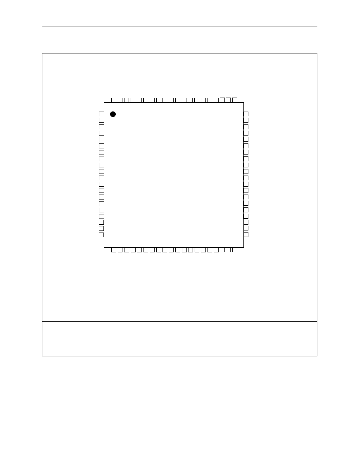
Bt8370/8375/8376 is packaged in an 80-pin Metric Quad Flat Pack (MQFP). A
pinout diagram of this device is illustrated in Figure 1-1. Figure 1-2 details a
Bt8370/8375/8376 logic diagram. Pin labels, names, I/O functions, and
descriptions are provided in Table 1-1.
The input pins listed below contain an internal pullup resistor (>50 kΩ) and
can remain unconnected if the active-high input state is desired. All other unused
input pins should be either pulled up or grounded.
1 A[7:0] Address lines unused in INTEL bus mode
2 XOE Active-high enables analog bipolar output
3 MOTO* Pullup selects INTEL bus mode if unconnected
1.1 Pin Assignments
4 SYNCMD Pullup selects synchronous processor interface
5 RCKI Receive clock unused if analog inputs enabled
6 TDI Unused if JTAG not connected
7 TMS Disables JTAG if not connected
8 TCK Unused if JTAG not connected
9 RST* Disables hardware reset if not connected
10 TDLI Unused if no external data link
11 TSIGI Unused if signaling data not supported by system
bus
N8370DSE
Conexant
1-1
Page 18
1.0 Pin Descriptions
Bt8370/8375/8376
1.1 Pin Assignments
Figure 1-1. Bt8370/8375/8376 Pinout Diagram
SIGFRZ
XOE
MOTO*
DTACK*
RCKI
80797877767574737271706968676665646362
SYNCMD
CS*
INTR*
DS* (RD*)
AS* (ALE)
R/W*(WR*)
VDD[0]
GND[0]
A[0]
AD[0]
A[1]
AD[1]
A[2]
AD[2]
A[3]
AD[3]
A[4]
AD[4]
A[5]
AD[5]
1
2
3
4
5
6
7
8
9
10
11
12
13
14
15
16
17
18
19
20
2122232425262728293031323334353637
GND[6]
RRING
RTIP
VDD[6]
RNEGI
RPOSI
VDD[5]
Bt8370/8375/8376
80-Pin MQFP
Fully Integrated T1/E1 Framer and Line Interface
(3)
TCKI
TCKO
GND[5]
GND[4]
38
39
VSET
61
60
59
58
57
56
55
54
53
52
51
50
49
48
47
46
45
44
43
42
41
40
VDD[4]
VDD[3]
XTIP
XRING
GND[3]
TDI
TDO
TCK
TMS
ACKI
VDD[2]
GND[2]
RCKO
RPOSO/RDLO
RNEGO/RDLCKO
RSBCKI
RMSYNC
RFSYNC
RPCMO
TPOSI/TDLI
REFCKI
CLADI
CLADO (NC)
A[6]
A[7]
AD[6]
A[8]
AD[7]
RST*
MCLK
VDD[1]
CLKMD
TPOSO/TNRZO/TINDO
GND[1]
ONESEC
TSIGI
TPCMI
TFSYNC
TMSYNC
NOTE(S):
1. Default pin assignments listed first for pins with multiple modes.
2. Motorola-style processor pin names listed first with Intel pins in parentheses.
3. Pin 66 is not connected for the Bt8376 device.
TSBCKI
TNEGI/TDLCKO
TNEGO/MSYNCO/RINDO
RSIGO
1-2
Conexant
N8370DSE
Page 19
Bt8370/8375/8376
1.0 Pin Descriptions
Fully Integrated T1/E1 Framer and Line Interface
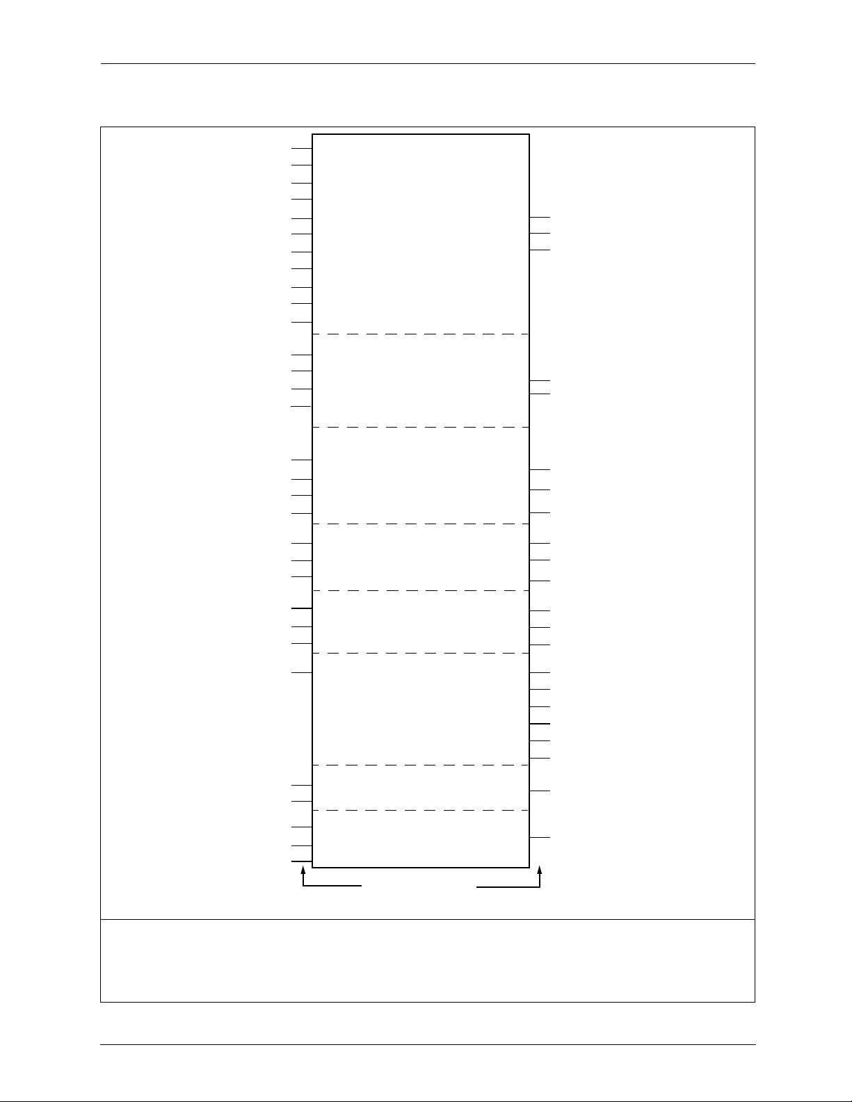
Figure 1-2. Bt8370/8375/8376 Logic Diagram
28
RST*
I/O
I/O
PIO
I
29
I
78
I
I
26
I
(1)
I
(1)
I
I
I
I
79
I
73
I
74
I
61
65
I
51
I
41
I
38
76
I
70
I
71
I
MCLK
MOTO*
1
SYNCMD
CLKMD
A[8:0]
AD[7:0]
5
AS* (ALE)
2
CS*
4
DS* (RD*)
6
R/W*(WR*)
XOE
RTIP
RRING
VSET
TCKI
ACKI
TPOSI/TDLI
TNEGI/TDLCKO
RCKI
RPOSI
RNEGI
Receive, Transmit
Hardware Reset
Processor Clock
Motorola Bus mode
Sync Bus mode
Clock mode
Address Bus
Data Bus or Address/Data
Address Strobe
Chip Select
Read or Data Strobe
Write Strobe or Read/Write
Transmit Output Enable
Receive Tip
Receive Ring
Voltage Reference Set
Tx Clock In
All Ones Clock
Tx Positive In/TDL Data In
Tx Negative In/TDL Clock
Rx Clock In
Rx Positive In
Rx Negative In
Microprocessor
Interface
(MPU)
Line Interface
(RLIU, TLIU)
Digital
Transmitter
(XMTR)
TNEGO/MSYNCO
Digital
Receiver
(RCVR)
RNEGO/RDLCKO
ONESEC
INTR*
DTACK*
XTIP
XRING
TCKO
TPOSO/TNRZO
RCKO
RPOSO/RDLO
1.1 Pin Assignments
PIO
32
3
77
58
57
64
27
39
48
47
46
1-second Timer
O
Interrupt Request
O
Data Transfer Acknowledge
O
Transmit Tip
O
Transmit Ring
Tx Clock Output
O
O
Tx Positive Out/Tx NRZ Data
Tx Negative Out/
O
Tx Multiframe Sync
O
Rx Clock Out
O
Rx Positive Out/RDL Data Out
O
Rx Negative Out/RDL Clock Out
(2)
(2)
37
TSBCKI
TSB Clock
TSB Data
TSB Signaling
RSB Clock
I
34
TPCMI
I
33
TSIGI
I
45
RSBCKI
I
Transmit
System Bus
(TSB)
TFSYNC
TMSYNC
RPCMO
Receive
System Bus
(RSB)
CLADI
CLAD In
Reference Clock
Test Clock I
Test Mode Select I
Test Data In I
NOTE(S):
(1)
Refer to Figure 1-1
(2)
Pins 27 and 39 shown twice for clarity; pin function controlled by PIO (addr 018).
(3)
Pin 66 is not connected for the Bt8376 device.
Bt8370/8375/8376 Pinout Diagram
67
I
REFCKI
68
I
TCK
53
52
TMS
55
TDI
Clock Rate
Adapter (CLAD)
Boundary Scan
(JTAG)
I = Input, O = Output,
PIO = Programmable I/O; controls located at PIO (address 018)
.
RFSYNC
RMSYNC
SIGFRZ
CLADO
TINDO
RSIGO
RINDO
TDO
O
27
35
36
42
40
39
43
44
80
66
54
TSB Time Slot Indicator
PIO
TSB Frame Sync
PIO
TSB Multiframe Sync
O
RSB Data Out
O
RSB Signaling Out
O
RSB Time Slot Indicator
PIO
RSB Frame Sync
PIO
RSB Multiframe Sync
O
Signaling Freeze
O
CLAD Out (NC)
O
Test Data Out
(2)
(2)
(3)
N8370DSE
Conexant
1-3
Page 20

1.0 Pin Descriptions
Bt8370/8375/8376
1.1 Pin Assignments
Table 1-1. Hardware Signal Definitions
(1 of 8)
Fully Integrated T1/E1 Framer and Line Interface
Pin Label Signal Name I/O Definition
Microprocessor Interface (MPU)
RST* Hardware Reset I RST* low-to-high transition forces registers to their default, power-up
state and forces all PIO pins to the input state. RST* is not mandatory,
because internal power on reset circuit performs an identical function.
RST* can be applied asynchronously, but must remain asserted for a
minimum of 2 clock cycles (ext ernal MCLK or internal 32 MHz) fo r th e
low-to-high transition to be sampled and detected (see also [RESET; addr
001]).
MCLK Processor Clock I System applies MCLK in the range of 8–36 MHz for external clock
(CLKMD = 1) and synchronous bus modes (SYNCMD = 1). During internal
clock modes (CLKMD = 0), the Bt8370/8375/8376 uses an internally
generated 32 MHz clock to control processor timing, and MCLK input is
ignored.
MOTO* Motorola Bus mode I Selects Intel- or Motorola-style microprocessor interface. DS*, R/W*,
A[8:0], and AD[7:0] functions are affected.
0 = Motorola; AD[7:0] is data, A[8:0] is address, DS* is data strobe,
and R/W* indicates the read (high) or write (low) data direction.
1 = Intel; AD[7:0] is multiplexed address/data, A[7:0] ignored, A[8] is
address line, DS* is read strobe (RD*), and R/W* is write strobe (WR*).
SYNCMD Sync mode I Selects whether read/write cycle timing is synchronous with MCLK.
Supports Intel- or Motorola-style buses:
0 = Asynchronous bus; read data enable and write data input latch are
asynchronously controlled by CS*, DS*, and R/W* signals. Latched write
data is still synchronized internally to 32 MHz clock for transfer to
addressed register.
1 = Synchronous bus; applicable only if the external clock is also
selected (CLKMD = 1). MCLK rising edge samples CS*, DS*, and R/W* to
determine valid read/write cycle timing. Allows 0 wait state processor
cycles for MCLK speeds up to 36 MHz, for M68000 type buses.
CLKMD Clock mode I Selects whether MCLK is enabled (high) or ignored (low). When enabled,
MCLK frequency determines update rate of internal registers and sampling
rate of CS*, DS*, and R/W* signals.
A[8:0] Address Bus I AS* fa lling edge asynchronously latches A[8:0] (Motorola) or A[8] (Intel)
to identify 1 register for subsequent read/write data transfer cycle.
AD[7:0] Data Bus or Address
Data
AS* (ALE) Address Strobe I For al l pro ces sor bus modes, AS* falling edge asynchronously latches
CS* Chip Select I Active-low enables read/write decoder. Active-high ends current read or
I/O Multiplexed address/data (Intel) or only data (Motorola). Refer to MOTO*
signal definition.
address from A[8:0] (Motorola) or from A[8] and AD[7:0] (Intel). For sync
modes (SYNCMD = 1), each read/write data cycle requires both AS* and
CS* active-low on MCLK rising edge.
write cycle and places data bus output in high impedance.
DS*(RD*) Data Strobe or
Read Strobe
R/W*(WR*) Read/Write Direction
or Write Strobe
1-4
I Active-low read data strobe (RD*) for MOTO* = 1, or read/write data
strobe (DS*) for MOTO* = 0.
I Active-low write data strobe (WR*) for MOTO* = 1, or read/write data
select (R/W*) for MOTO = 0.
Conexant
N8370DSE
Page 21

Bt8370/8375/8376
1.0 Pin Descriptions
Fully Integrated T1/E1 Framer and Line Interface
Table 1-1. Hardware Signal Definitions
(2 of 8)
1.1 Pin Assignments
Pin Label Signal Name I/O Definition
Microprocessor Interface (MPU) (Continued)
ONESEC 1-second Timer PIO Controls or marks 1-second interval used for status reporting. When
input, the timer is aligned to ONESEC rising edge. When output, rising
edge indicates start of each 1-second interval. Typically, 1 device in a
multi-line system is configured to output ONESEC to synchronize other
Bt8370/8375/8376 status reports on a common 1-second interval.
INTR* Interrupt Request O Open drain active-low output signifies 1 or more pending interrupt
requests. INTR* goes to high-impedance state after processor has
serviced all pending interrupt requests.
DTACK* Data Transfer
Acknowledge
O Open drain active-low output signifies in-progress data transfer cycle.
DTACK* remains asserted (low) for as long as AS* and CS* are both
active-low. DTACK* is only implemented during synchronous Motorola
processor interface modes. Refer to the timing diagrams in Section 5.5,
MPU Interface Timing
.
Line Interface Unit (LIU)
XOE Transmit Output
Enable
I Active-high input enables XTIP and XRING output drivers; otherwise, both
outputs are placed in high-impedance state. XOE contains internal pullup
so systems that do not require three-stated outputs can leave XOE
unconnected. XOE needs to be disabled during Power-On Reset (POR) and
re-enabled after configuring the part. Refer to Power-On Reset procedure
in Section 2.10.4,
Device Reset
.
RTIP, RRING Receive Tip/Ring I D ifferential AMI data inputs for direct connection to receive transformer.
VSET Voltage Reference Set I/O Constant voltage output. Must be connected to an external 1% resistor
equal to 14 kΩ to ground (GND[4] pin 62). The VSET resistor sets the
internal precision current reference of 100 µA and also controls the
transmit pulse height.
XTIP, XRING Transmit Tip/Ring O Com plementary AMI data outputs for direct connection to transmit
transformer. Optionally, both outputs are three -stated when XOE is
negated.
Digital Transmitter (XMTR)
TCKI Tx Clock Input I Primary TX line rate clock applied on TCKI, or the system chooses from 1
of four different clocks to act as TX clock source (see [CMUX; addr 01A]).
The selected source is used to clock digital transmitter signals TPOSI,
TNEGI, TPOSO, TNEGO, TNRZO, MSYNCO, TDLI, and TDLCKO. If TSLIP is
bypassed, selected source also clocks TSB signals.
ACKI All Ones Clock I System optionally applies ACKI for AIS transmission, if the selected
primary transmit clock source fails. ACKI is either manually or
automatically switched to replace TCKI (see [AISCLK; addr 068]). Systems
without an AIS clock must tie ACKI to ground.
N8370DSE
Conexant
1-5
Page 22

1.0 Pin Descriptions
Bt8370/8375/8376
1.1 Pin Assignments
Table 1-1. Hardware Signal Definitions
(3 of 8)
Fully Integrated T1/E1 Framer and Line Interface
Pin Label Signal Name I/O Definition
Digital Transmitter (XMTR) (Continued)
TPOSI TX Positive Rail Input I Line rate data input on TCKI falling edge. Replaces all data that would
otherwise be supplied by ZCS encoder. Bt8370/8375/8376 default power
on state selects TPOSI/TNEGI as source for all transmitted XTIP/XRING
output pulses, encoded as follows:
TPOSI TNEGI TX Pulse Polarity
0 0 No pulse
0 1 Negative AMI pulse
1 0 Positive AMI pulse
11Invalid
NOTE(S):
data from internal transmitter.
TNEGI TX Negative Rail Input I Line rate data input on TCKI falling edge. Replaces all data that would
otherwise be supplied by ZCS encoder. Refer to TPOSI signal definition.
TPOSO TX Positive Rail
Output
O Line rate data output from ZCS encoder or JAT on rising edge of TCKO.
Active-high marks transmission of a positive AMI pulse. Used to monitor
transmit data or for systems that employ an external line interfac e unit.
Software must set TDL_IO (addr 018) to enable normal
TNEGO TX Negative Rail
Output
TDLI TX Data Link Input I Selected time slot bits are sampled on TDLCKO falling edge for insertion
TDLCKO TX Data Link Clock O Gapped version of TCKI for external data link applications. TDLCKO high
TCKO TX Clock Output O Line rate clock used to align XTIP/XRING outputs. If transmit jitter
TNRZO TX Non Return to
Zero Data
MSYNCO TX Multiframe Sync O Active-high for 1 TCKI clock cycle to mark the first bit of TX multiframe
O Line-rate data output from ZCS encoder or JAT on rising edge of TCKO.
Active-high marks transmission of a negative AMI pulse. Used to monitor
transmit data or for systems that use an external line interface uni t.
into the transmit output stream during external data link applications.
clock pulse coincides with low TCKI pulse interval during selected time
slot bits (see [DL3_TS; addr 015]).
attenuator (TJAT) is disabled, TCKO equals selected TCKI or ACKI. If TJAT
is enabled, TCKO equals the jitter attenuated clock (JCLK).
O Line rate data output from transmitter on rising edge of TCKI. TNRZO does
not include ZCS encoded bipolar violations.
coincident with TNRZO. Output on rising edge of TCKI.
1-6
Conexant
N8370DSE
Page 23

Bt8370/8375/8376
1.0 Pin Descriptions
Fully Integrated T1/E1 Framer and Line Interface
Table 1-1. Hardware Signal Definitions
(4 of 8)
1.1 Pin Assignments
Pin Label Signal Name I/O Definition
Digital Receiver (RCVR)
RCKI RX Clock Input I Line rate clock samples RPOSI and RNEGI when RLIU configured to
accept dual-rail digital data (see [RDIGI; addr 020]); otherwi se, RCKI is
ignored.
RPOSI RX Positive Rail Input I Line rate data input on falling edge of RCKI. RPOSI and RNEGI levels are
interpreted as received AMI pulses, encoded as follows:
RPOSI RNEGI RX Pulse Polarity
0 0 No pulse
0 1 Negative AMI pulse
1 0 Positive AMI pulse
1 1 Invalid
The NRZ data can be input at RPOSI or RNEGI if the
NOTE:
other input is connected to ground.
RNEGI RX Negative Rail
Input
I Line rate data input on falling edge of RCKI. See RPOSI signal definition.
RCKO RX Clock Output O RPLL rec ove red line rate clock (RXCLK) or jitter attenuated clock (JCLK)
output, based on programmed clock selection (see [JAT_CR; addr 002]).
RPOSO RX Positive Rail
Output
RNEGO RX Negative Rail
Output
RDLO RX Data Link Output O Line rate NRZ data output from receiver on falling edge of RCKO, all data
RDLCKO RX Data Link Clock
Output
O Line rate data output on rising edge of RCKO. Active-high indicates receipt
of a positive AMI pulse on RTIP/RING inputs.
O Line rate data output on rising edge of RCKO. Active-high indicates receipt
of a negative AMI pulse on RTIP/RING inputs.
from RLIU is represented at the RDLO pin. However, selective RDLO bit
positions are also marked by RDLCKO for external data link applications.
O Gapped version of RCKO for external data link applications. RDLCKO high
clock pulse coincides with low RCKO pulse interval during selected time
slot bits, else RDLCKO low (see Figure 2-12,
Waveforms
, External Data Link).
Receive External Data Link
N8370DSE
Conexant
1-7
Page 24

1.0 Pin Descriptions
Bt8370/8375/8376
1.1 Pin Assignments
Table 1-1. Hardware Signal Definitions
(5 of 8)
Fully Integrated T1/E1 Framer and Line Interface
Pin Label Signal Name I/O Definition
Transmit System Bus (TSB)
TSBCKI TSB Clock Input I Bit clock and I/O signal timing for TSB according to system bus mode (see
[SBI_CR; addr 0D0]). System chooses from 1 of four different clocks to
act as TSB clock source (see [CMUX; addr 01A]). Rising or falling edge
clocks are independently configurable for data signals TPCMI, TSIGI ,
TINDO and sync signals TFSYNC and TMSYNC (see [TPCM_NEG and
TSYN_NEG; addr 0D4]). When configured to operate at twice the data rate,
TSB clock is internally divided by two before clocking TSB data signals.
TPCMI TSB Data Input I Serial data formatted into TSB frames consisting of DS0 channel time
slots and optional F-bits. One group of 24 T1 time slots or 32 E1 time slots
is selected from up to four available groups; data from the group is
sampled by TSBCKI, then sent towards transmitter output. Time slots are
routed through transmit slip buffer (see [TSLIPn; addr 140–17F])
according to TSLIP mode (see [TSBI; addr 0D4]). F-bits are taken from the
start of each TSB frame or from within an embedded time slot (see
[EMBED; addr 0D0]) and optionally inserted into the transmitter output
(see [TFRM; addr 072] register).
TSIGI TSB Signaling Input I Serial data formatted into TSB frames containing ABCD signaling bits for
each system bus time slot. Four bits of TSIGI time slot carry signalin g
state for each accompanying TPCMI time slot. Signaling state of every
time slot is sampled during first frame of the TSB multiframe, and then
transferred into transmit signaling buffer [TSIGn; addr 120–13F].
TINDO TSB Time Slot
Indicator
TFSYNC TSB Frame Sync PIO Input or output TSB frame sync (se e [TFSYNC_IO; addr 018]). TFSYNC
TMSYNC TSB Multiframe Sync PIO Input or output TSB multiframe sync (see [TMSYNC_IO; ad dr 018]).
O Acti ve-high output pulse marks selective transmit system bus time slots
as programmed by SBCn [addr 0E0–0FF]. TINDO occurs on TSBCKI rising
or falling edges as selected by TPCM_NEG (see [TSBI; addr 0D4]).
output is active-high for 1 TSB clock cycle at programmed offset bit
location (see [TSYNC_BIT; addr 0D5]), marking offset bit position within
each TSB frame and repeating once every 125 µs. When transmit framer is
also enabled, TSB timebase and TFSYNC output frame alignment are
established by transmit framer's examination of TPCMI serial data input.
When TFSYNC is programmed as an input, t he lo w-t o-high signal
transition is detected and aligns TSB timebase to programmed offset bit
value. TSB timebase flywheels at 125 µs frame interval after the last
TFSYNC is applied.
TMSYNC output is active-high for 1 TSB clock cycle at programmed offset
bit location (see [TSYNC_BIT; addr 0D5]), marking offset bit position
within each TSB multiframe and repeating once every 6 ms coincident
with TFSYNC. When transmit framer is also enabled, TSB timebase and
TMSYNC output multiframe alignment are established by transmit
framer's examination of TPCMI serial data input. When TMSY NC is
programmed as an input, the low-to-high signal transition is detected and
aligns TSB timebase to the programmed offset bit value and first frame of
the multiframe. TSB timebase flywheels at 6 ms multiframe interval after
the last TMSYNC is applied. If system bus applies TMSYNC input, TFSYNC
input is not needed.
1-8
Conexant
N8370DSE
Page 25

Bt8370/8375/8376
1.0 Pin Descriptions
Fully Integrated T1/E1 Framer and Line Interface
Table 1-1. Hardware Signal Definitions
(6 of 8)
1.1 Pin Assignments
Pin Label Signal Name I/O Definition
Receive System Bus (RSB)
RSBCKI RSB Clock Input I Bit clock and I/O signal timing for RSB according to system bus mode (see
[SBI_CR; addr 0D0]). System chooses from 1 of four different clocks to
act as RSB clock source (see [CMUX; addr 01A]). Rising or falling edge
clocks are independently configurable for data signals RPCMO, RSIGO,
RINDO and sync signals RFSYNC, RMSYNC (see [RPCM_NEG and
RSYN_NEG; addr 0D1]). When configured to operate at twice the data
rate, RSB clock is internally divided by 2 before clocking RSB data signals.
RPCMO RSB Data Outp ut O Serial data formatted into RSB frames consisting of DS0 channel time
slots, optional F-bits, and optional ABCD signaling. Time slots are routed
through receive slip buffer (see [RSLIPn; addr 1C0–1FF]) according to
RSLIP mode (see [RSBI; addr 0D1]). Data for each output time slot is
assigned sequentially from received time slot data according to system
bus channel programming (see [ASSIGN; addr 0E0–0FF]). F-bits are
output at the start of each RSB frame or at the embedded time slot
location (see [EMBED; addr 0D0]). ABCD signaling is optionally inserted
on a per-channel basis (see [INSERT; addr 0E0–0FF]) from the local
signaling buffer (see [RLOCAL; addr 180–19F]) or from the receive
signaling buffer [RSIGn; addr 1A0–1BF]. When enabled, robbed bit
signaling or CAS reinsertion is performed according to T1/E1 mode: the
eighth time slot bit of every sixth T1 frame is replaced, or the 4-bit
signaling value in the E1 time slot 16 is replaced.
RSIGO RSB Signaling Output O Serial data formatte d into RSB frames consisting of ABCD signaling bits
for each system bus time slot. Four bits of RSIGO time slot carry signaling
state for each accompanying RPCMO time slot. Local or through signaling
bits are output in every frame for each time slot and updated once per RSB
multiframe, regardless of per-channel RPCMO signaling reinsertion.
RINDO RSB Time Slot
Indicator
RFSYNC RSB Frame Sync PIO Input or output RSB frame sync (see [RFSYNC_IO; addr 018]). RFSYNC
RMSYNC RSB Multiframe Sync PIO Input or output RSB multiframe sync (see [RMSYNC_IO; addr 018]).
O Active-high output pulse marks selective receive system bus time slots as
programmed by SBCn [addr 0E0–0FF]. RINDO occurs on RSBCKI rising or
falling edges as selected by RPCM_NEG (see [RSBI; addr 0D1]).
output is active-high for 1 RSB clock cycle at programmed offset bit
location (see [RSYNC_BIT; addr 0D2]), marking offset bit within each RSB
frame and repeating once every 125 µs. RSB timebase and RFSYNC
output frame alignment begins at an arbitrary position and ch anges
alignment according to RSLIP mode (see [RSBI; addr 0D1]). When
RFSYNC is programmed as an input, the low-to-high signal transition is
detected and aligns RSB timebase to the programmed offset. RSB
timebase flywheels at 125 µs frame interval after the last RFSYNC is
applied.
RMSYNC output is active-high for 1 RSB clock cycle at programmed offset
bit location (see [RSYNC_BIT; addr 0D2]), marking offset bit within each
RSB multiframe and repeating once every 6 ms coinciding with RFSYNC.
RSB timebase and RMSYNC output multiframe alignment begins at an
arbitrary position and changes alignment according to RSLIP mode (see
[RSBI; addr 0D1]). When RMSYNC is programmed as input, the
low-to-high signal transition is detected and aligns the RSB timebase to
the programmed offset and the first frame of the multiframe. RSB
timebase flywheels at 6 ms multiframe interval after the last RMSYNC is
applied.
N8370DSE
Conexant
1-9
Page 26

1.0 Pin Descriptions
Bt8370/8375/8376
1.1 Pin Assignments
Table 1-1. Hardware Signal Definitions
(7 of 8)
Fully Integrated T1/E1 Framer and Line Interface
Pin Label Signal Name I/O Definition
Receive System Bus (RSB) (Continued)
SIGFRZ Signaling Freeze O Active-high indicates that signaling bit updates are suspended for both
receive signaling buffer [RSIGn; addr 1A0–1BF] and stack [STACK; addr
0DA] register. SIGFRZ, clocked by RSB clock, goes high coinciding with
receive loss of frame alignment (see RLOF; addr 047) and returns low 6–9
ms after recovery of frame alignment.
NOTE(S):
1. All RSB and TSB outputs can be placed in high-impedance state (see SBI_OE; addr 0D0).
2. Receive System Bus (RSB)
1-10
Conexant
N8370DSE
Page 27

Bt8370/8375/8376
1.0 Pin Descriptions
Fully Integrated T1/E1 Framer and Line Interface
Table 1-1. Hardware Signal Definitions
(8 of 8)
1.1 Pin Assignments
Pin Label Signal Name I/O Definition
Clock Rate Adapter (CLAD)
CLADI CLAD Input I Optional CLAD input timing reference used to phase lock CLADO and JCLK
outputs to 1 of 44 different input clock frequencies selected in the range of
8 kHz to 16384 kHz (see [CLAD registers; addr 090–092]).
REFCKI Reference Clock I System must apply a 10 MHz ±50 ppm clock signal to act as frequency
reference for internal Numerical Controlled Oscillator (NCO). REFCKI
determines frequency accuracy and stability of CLADO and jitter attenuator
(JCLK) clocks when the NCO operates in free running mode (see [JFREE;
addr 002]).
REFCKI is the baseband reference for all CLAD/JA T functions and is used
internally to generate clocks of various freq uencies, l ocke d to a sele cte d
receive, transmit, or external clock. Hence, REFCKI is always required.
CLADO CLAD Output O CLADO is configured to operate at 1 of 14 different clock frequencies (see
[CSEL; addr 091]) that include T1, E1 or system bus rates. CLADO is
typically programmed to supply RSB and TSB clocks that are
phase-locked to the selected transmit, receive or CLADI timing reference
(see [JEN; addr 002 and CEN; addr 090]). On the Bt8376 device, CLAD0
drives low when enabled.
Test Access
TDI JTAG Test Data Input I Test data input per
instructions and data into internal test logic. Sampled on the rising edge of
TCK. TDI can be left unconnected if it is not being used because it is pulled
up internally.
TMS JTAG Test mode
Select
TDO JTAG Test Data
Output
TCK JTAG Test Clock I Test clock input per IEEE Std 1149.1-1 990. Used for all test interface and
I Active-low test mode select input per
pulled-up input signal used to control the test-logic state machine.
Sampled on the rising edge of TCK. TMS can be left unconnected if it is
not being used because it is pulled up internally.
O Test data output per
reading all serial configuration and test data from internal test logic.
Updated on the falling edge of TCK.
internal test-logic operations. If unused, TCK must be pulled low.
IEEE Std 1149.1-1990
IEEE Std 1149.1-1990
IEEE Std 1149.1-1990
. Used for loading all serial
. Internally
. Three-state output used for
Power Supply
VDD[6:0] Power I +5 VDC ±5%
GND[6:0] Ground I 0 VDC
NOTE(S):
1. I = Input, O = Output
2. PIO = Programmable I/O; controls located at address 018.
3. Multiple signal names show mutually exclusive pin functions.
4. All output pins power up in the high-impedance state within 3,000 cycles of the applied REFCKI (see POE; addr 019,
SBI_OE; addr 0D0).
N8370DSE
Conexant
1-11
Page 28

1.0 Pin Descriptions
Bt8370/8375/8376
1.1 Pin Assignments
Fully Integrated T1/E1 Framer and Line Interface
1-12
Conexant
N8370DSE
Page 29

2
2.0 Circuit Description
2.1 Bt8370/8375/8376 Block Diagrams
Detailed block diagrams are illustrated in Figure 2-1 (Bt8370), Figure 2-2
(Bt8375), and Figure 2-3 (Bt8376). To show the details of this circuit, individual
block diagrams, along with descriptions, appear throughout this section.
1. Receive Line Interface Unit (RLIU)
2. Jitter Attenuator (JAT)
3. Digital Rece iver (RCVR)
4. Receive System Bus (RSB)
5. Clock Rate Adapter (CLAD)
6. Transmit System Bus (TSB)
7. Digital Transmitter (XMTR)
8. Transmit Line Interface Unit (TLIU)
9. Microprocessor Interface (MPU)
10. Joint Test Access Group Port (JTAG)
NOTE:
The Bt8375 differs from the Bt8370 only in that the Bt8375 does not have
LBO filters in the transmit LIU. The Bt8376 differs from Bt8375 in that
Bt8376 has neither a CLADO output, nor a DLINK2.
N8370DSE
Conexant
2-1
Page 30
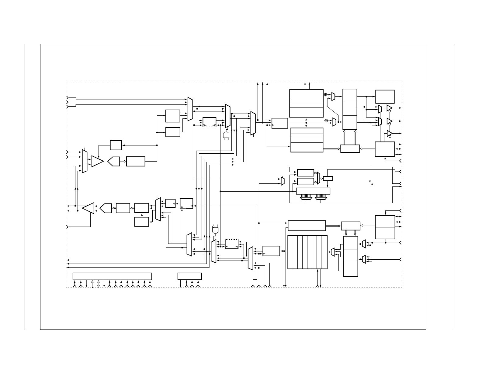
2-2
Figure 2-1. Detailed Bt8370 Block Diagram
2.1 Bt8370/8375/8376 Block Diagrams
2.0 Circuit Description
Conexant
RPOSI
RNEGI
RCKI
RTIP
RRING
XTIP
XRING
XOE
TPOSO
TNEGO
TCKO
ALOOP
0
VGA
1
Loopback
Analog
DAC
DRV
Microprocessor Port
AGC
ADC
LBO
Filters
Adaptive
Equalizer
Pulse
Shape
8X
TPLL
TAIS
1
0
Data
Slicer
RPLL
AIS
1
0
RDIGI
LLOOP
Clock
Mon
LLOOP
1
0
JTAG Port
RJAT
JDIR
1
0
JEN
0
1
JEN
JDIR
FLOOP
TJAT
RPOSO
0
1
FLOOP
TDL_IO
1
0
RNEGO
RCKO
RXCLK
TXCLK
JCLK
TZCS
Encode
RZCS
Decode
JDIR
1
0
RDLCKO
RDLO
External DLINK
PRBS/Inband LB
DLINK 2 Buffer
DLINK 1 Buffer
Sa-Byte/BOP
PDV Monitor
Error Counters
Alarm Monitor
Receive Framer
Receiver
Timebase
CPHASE
JPHASE
Divider Chain
Transmitter
Timebase
Alarm/Error Insert
PRBS/Inband LB
DLINK 2 Buffer
PVD Enforcer
DLINK 1 Buffer
Sa-Byte/BOP
NCO
T1/E1 Frame Insert
External DLINK
AIS
RSIG
Buffer
RSIG
Local
RSLIP
Buffer
RPHASE
PLOOP
TPHASE
TSLIP
Buffer
TSIG
Buffer
TSIG
Local
OR
TLOOP
RSIG
STACK
RSB
Timebase
RLOOP
TSB
Timebase
Transmit
Framer
RSIGO
RPCMO
SIGFRZ
RINDO
RFSYNC
RMSYNC
RSBCKI
REFCKI
CLADI
CLADO
TSBCKI
TFSYNC
TMSYNC
TINDO
TPCMI
TSIGI
Fully Integrated T1/E1 Framer and Line Interface
Bt8370/8375/8376
N8370DSE
RST*
ONESEC
INTR*
A[8:0]
DTACK*
AD[7:0]
R/W*
DS*
AS*
CS*
MOTO*
CLKMD
SYYNCMD
MCLK
TDO
TDI
TMS
TCK
ACKI
TCKI
TPOSI
TNEGI
MSYNCO
TNRZO
TDLI
TDLCKO
Page 31

N8370DSE
Figure 2-2. Detailed Bt8375 Block Diagram
Bt8370/8375/8376
Fully Integrated T1/E1 Framer and Line Interface
Conexant
RPOSI
RNEGI
RCKI
RTIP
RRING
XTIP
XRING
XOE
TPOSO
TNEGO
TCKO
ALOOP
0
VGA
1
Loopback
Analog
DRV
Microprocessor Port
AGC
ADC
DAC
Adaptive
Equalizer
Pulse
Shape
TPLL
8X
RNEGO
RPOSO
RCKO
1
Data
Slicer
RPLL
TAIS
AIS
1
0
0
RDIGI
LLOOP
Clock
Mon
LLOOP
1
0
JTAG Port
RJAT
JDIR
1
0
JEN
0
1
JEN
JDIR
FLOOP
TJAT
0
1
FLOOP
TDL_IO
1
0
RXCLK
TXCLK
JCLK
TZCS
Encode
RZCS
Decode
JDIR
1
0
RDLCKO
RDLO
External DLINK
PRBS/Inband LB
DLINK 2 Buffer
DLINK 1 Buffer
Sa-Byte/BOP
PDV Monitor
Error Counters
Alarm Monitor
Receive Framer
Receiver
Timebase
CPHASE
JPHASE
Divider Chain
Transmitter
Timebase
Alarm/Error Insert
PRBS/Inband LB
DLINK 2 Buffer
PVD Enforcer
DLINK 1 Buffer
Sa-Byte/BOP
AIS
NCO
T1/E1 Frame Insert
External DLINK
RSIG
Buffer
RSIG
Local
RSLIP
Buffer
RPHASE
PLOOP
TPHASE
TSLIP
Buffer
TSIG
Buffer
TSIG
Local
or
TLOOP
RSIG
STACK
RSB
Timebase
RLOOP
TSB
Timebase
Transmit
Framer
RSIGO
RPCMO
SIGFRZ
RINDO
RFSYNC
RMSYNC
RSBCKI
REFCKI
CLADI
CLADO
TSBCKI
TFSYNC
TMSYNC
TINDO
TPCMI
TSIGI
2.1 Bt8370/8375/8376 Block Diagrams
2.0 Circuit Description
2-3
RST*
ONESEC
INTR*
A[8:0]
DTACK*
AD[7:0]
R/W*
DS*
AS*
CS*
CLKMD
SYYNCMD
MOTO*
MCLK
TDO
TDI
TMS
TCK
ACKI
TCKI
TPOSI
TNEGI
MSYNCO
TNRZO
TDLI
TDLCKO
Page 32

2-4
Figure 2-3. Detailed Bt8376 Block Diagram
2.1 Bt8370/8375/8376 Block Diagrams
2.0 Circuit Description
Conexant
RPOSI
RNEGI
RCKI
RTIP
RRING
XTIP
XRING
XOE
TPOSO
TNEGO
TCKO
ALOOP
0
VGA
1
Loopback
Analog
DRV
Microprocessor Port
AGC
ADC
DAC
Adaptive
Equalizer
Pulse
Shape
8X
TPLL
RNEGO
RPOSO
RCKO
1
Data
Slicer
RPLL
TAIS
AIS
1
0
0
RDIGI
LLOOP
Clock
Mon
LLOOP
1
0
JTAG Port
RJAT
JDIR
1
0
JEN
0
1
JEN
JDIR
FLOOP
TJAT
0
1
FLOOP
TDL_IO
1
0
RXCLK
TXCLK
JCLK
TZCS
Encode
RZCS
Decode
JDIR
1
0
RDLCKO
RDLO
External DLINK
PRBS/Inband LB
DLINK 1 Buffer
Sa-Byte/BOP
PDV Monitor
Error Counters
Alarm Monitor
Receive Framer
Receiver
Timebase
CPHASE
JPHASE
Divider Chain
Transmitter
Timebase
Alarm/Error Insert
PRBS/Inband LB
External DLINK
PVD Enforcer
DLINK 1 Buffer
Sa-Byte/BOP
T1/E1 Frame Insert
NCO
AIS
RSIG
Buffer
RSIG
Local
RSLIP
Buffer
RPHASE
PLOOP
TPHASE
TSLIP
Buffer
TSIG
Buffer
TSIG
Local
or
TLOOP
RSIG
STACK
RSB
Timebase
RLOOP
TSB
Timebase
Transmit
Framer
RSIGO
RPCMO
SIGFRZ
RINDO
RFSYNC
RMSYNC
RSBCKI
REFCKI
CLADI
TSBCKI
TFSYNC
TMSYNC
TINDO
TPCMI
TSIGI
Fully Integrated T1/E1 Framer and Line Interface
Bt8370/8375/8376
N8370DSE
RST*
ONESEC
INTR*
A[8:0]
DTACK*
AD[7:0]
R/W*
DS*
AS*
CS*
CLKMD
MOTO*
MCLK
SYYNCMD
TDO
TDI
TMS
TCK
ACKI
TCKI
TNEGI
TPOSI
MSYNCO
TNRZO
TDLI
TDLCKO
Page 33

Bt8370/8375/8376
2.0 Circuit Description
Fully Integrated T1/E1 Framer and Line Interface
2.2 Receive Line Interface Unit
The Receive Line Interface Unit (RLIU) reco vers clock and data from the bipolar
Alternate Mark Inv ersion (AMI) line signal that has been attenuated and distorted
due to the characteristics of the line. In the Bt8370 device, the RLIU is sensitive
to signals attenuated in the range of 0 to –48 dB in E1 and T1 modes. In the
Bt8375 and Bt8376 devices, RLIU sensitivity is limited for short-haul only
applications. In addition, the RLIU interfaces at the DSX-1 Bridge Monitor Level
(–20 dB for DS1 and –30 dB for E1/CEPT).
The RLIU converts AMI pulses into P and N rail Non-Return to 0 (NRZ) data.
The AMI pulses are input on the receive tip and ring pins: RTIP and RRING
(Figure 2-4). The P and N rail NRZ data is then passed to the RCVR. The RCVR
dual rail output is available on RPOSO/RNEGO. Figure 2-5 illustrates the
relationship between the AMI received signal, the recovered clock, and the
RCVR dual rail outputs.
Figure 2-4. RLIU Diagram
2.2 Receive Line Interface Unit
RPOSI
RPOSI
RNEGI
RNEGI
RTIP
RRING
RCKI
Analog Loopback
O
1
ALOOP
VGA
ADC
ADC
Adaptive
Equalizer
Data
Slicer
RPLL
RDIGI
1
O
1
O
To JAT
RJAT
O
1
From JAT
RPOSO
RNEGO
RXCLK
N8370DSE
Conexant
2-5
Page 34

2.0 Circuit Description
Bt8370/8375/8376
2.2 Receive Line Interface Unit
Figure 2-5. RLIU Waveforms—Bipolar Input Signal
RTIP ,
RRING
RXCLK
RPOSO
RNEGO
1
2
3
13 56
24
If the RLIU functionality is not required, a bypass mode is provided [RDIGI;
addr 020]. If the RLIU is bypassed, the RTIP/RRING pins are ignored,
RPOSI/RNEGI P and N rail NRZ become inputs, and RCKI becomes the receive
timing source. Figure 2-6 illustrates the relationship between the RLIU P and N
rail NRZ data, the RLIU receive clock input, and the RCVR dual rail output.
4
Throughput
Fully Integrated T1/E1 Framer and Line Interface
BPV
56
7
BPV
7
Figure 2-6. RLIU Waveforms—P and N Rail Digital Input Signal
RPOSI
RNEGI
RCKI
RPOSO
RNEGO
1
2
3
4
Throughput
1
2
3
BPV
56
7
56
4
BPV
7
2-6
Conexant
N8370DSE
Page 35

Bt8370/8375/8376
2.0 Circuit Description
Fully Integrated T1/E1 Framer and Line Interface
2.2.1 Data Recovery
The RLIU recovers data from the received analog signal by normalizing the
signal with the Variable Gain Amplifier (VGA) and the Automatic Gain Control
(AGC), removing distortion with the Adaptive Equalizer, and extracting the data
using the Data Slicer.
2.2.1.1 Automatic Gain Control
2.2.1.2 Variable Gain Amplifier
The AGC circuit adjusts the gain of the incoming dif ferential signal to achieve a
normalized level. The normalized le vel ensures that the input signal to the ADC is
75% to 100% of full scale. This is done by measuring the peak voltage of the
incoming signal with a peak detector , and in v ersely adjusting V GA gain based the
peak value. The AGC can be forced to a fixed gain for test purposes or limited to
a maximum value, which is the normal operating mode (see [FORCE_VGA;
addr 020]).
The FORCE_VGA bit in the LIU Configuration register [LIU_CR; addr 020]
selects whether the AGC operates in Gain Limit mode or Fixed Gain mode. In
Gain Limit modes, the RLIU sensitivity is initially set to the maximum
(approximately 43 dB), and the gain is adjusted based the peak value recorded
during the AGC obser vation period. Th e A GC observ ation period can be set to 32,
128, 512, or 2048 symbol periods [RLIU_CR; addr 022]. A short observation
period allows quick responses to pulse height variations but possible overshoots.
A long observation period minimizes overshoots, but does not react quickly to
pulse height variations. The real-time status of the VGA gain setting can be read
in the Variable Gain Amplifier Status register [VGA; addr 029] and used to
approximate the receive analog signal level.
In Fixed Gain mode, the RLIU sensitivit y is set to the value stored in the
Variable Gain Amplifier Maximum register [VGA_MAX; addr 024]. V GA_MAX
is a 6-bit register that allows up to 64 gain settings in 1. 25 dB steps.
2.2 Receive Line Interface Unit
2.2.1.3 Adaptive Equalizer
2.2.1.4 Data Slicer
After the input amplitude has been normalized, the adaptive equalizer attempts to
remove the distortion introduced by the cable. The transfer function of the
equalizer is initially adjusted based on the peak value of the input signal because
this value prov ides some indication of the line length on the input. The Adaptive
Equalizer then automatically fine tunes to remove most of the signal distortion
due to intersymbol interference, noise, and other cable length effects.
In certain applications the device can be connected to a DSX monitor point
that has been resistively attenuated. Because this resistive attenuation adds no
phase-versus-frequency distortion, the VGA gain must be adjusted. This is done
by configuring the Receive Pad Resistor Compensation (ATTN[1,0]) in the LIU
Configuration register [LIU_CR; addr 020]. The resistive attenuation can be
configured to be either 0, –10, –20, or –30 dB.
The Data Slicer extracts the data from the equalized signal by comparing the
differential inputs to threshold values. The threshold values are dynamically set,
based on a percentage of the peak level obtained by the peak detector. The
percentage is 50% of peak for both DS1 and CEPT. Dynamically adjusting the
threshold values ensures optimum signal-to-noise ratio. If the SQUELCH bit is
set in the LIU Configuration register [LIU_CR; addr 020] and the input signal
level is below threshold for the entire AGC observation period (EYEOPEN = 0),
Data Slicer output is forced to all 0s.
N8370DSE
Conexant
2-7
Page 36

2.0 Circuit Description
]
Bt8370/8375/8376
2.2 Receive Line Interface Unit
2.2.2 Clock Recovery
2.2.2.1 Phase Locked Loop
Figure 2-7. Receive Input Jitter Tolerance
10000
1000
138 UI
100
The Receive Phase Locked Loop (RPLL) recovers the line rate clock from the
Data Slicer dual rail outputs. The RPLL generates a recovered clock that tracks
the jitter in the data from the Data Slicer, and sustains the data-to-clock phase
relationship in the absence of incoming pulses. Figure 2-7 illustrates the Receive
LIU’s input clock and data jitter tolerance.
Data Jitter
Tolerance
TR 62411 (T1)
Min. Tolerance
Fully Integrated T1/E1 Framer and Line Interface
28 UI
10
1
Sine Wave Jitter Amplitude (UI pk-pk) [Log Scale]
0.1
0.1 1 10 100 1000 10000 100000
G. 824 (T1)
Min. Tolerance
Reg. G. 823 (E1)
Min. Tolerance
Sine Wa ve Jitter Frequency (Hz) [Log Scale
5 UI
1.5 UI
Clock Jitter
Tolerance
0.1UI
0.2UI
0.35 UI
.22 UI
2-8
Conexant
N8370DSE
Page 37

Bt8370/8375/8376
2.0 Circuit Description
Fully Integrated T1/E1 Framer and Line Interface
2.3 Jitter Attenuator
The Jitter Attenuator (JAT), illustrated in Figure 2-8, attenuates jitter in the
receive or tran smit path, but not both simultaneously. In the receive configuration,
the line signal is recovered by the RLIU and is dejittered before it is decoded by
the RCVR. In the transmit configuration, the encoded signal from the transmit
block is dejittered before it is transmitted by the Transmit Line Interface Unit
(TLIU). The JAT receive/transmit configuration is done through the JDIR bit in
the Jitter Attenuator Configuration register [JA T_CR; addr 002]. The JA T can also
be completely disabled using the Jitter Attenuation (JEN) bit in the JAT_CR
register.
Figure 2-8. Jitter Attenuator Block Diagram
From RLIU
To RLIU
Rin Rout
RJAT
or
TJAT
TinTout
Depth
JCLK
RXCLK
To JPHASE
2.3 Jitter Attenuator
(to CLAD)
To/From TLIU
TXCLK
JCLK
(from CMUX)
N8370DSE
Conexant
2-9
Page 38

2.0 Circuit Description
Bt8370/8375/8376
2.3 Jitter Attenuator
2.3.1 Elastic Store
Fully Integrated T1/E1 Framer and Line Interface
The elastic store size (RJAT or TJAT) is configurable using JSIZE[2:0] in the
JAT_CR. The elastic store sizes available are 8, 16, 32, 64, and 128 bits. The
32-bit elastic store depth is sufficient to meet jitter tolerance requirements in
cases where the jitter attenuator cutoff frequency is programmed at 6 Hz or below ,
and when the selected clock reference is frequency-locked. The larger elastic
store depths allows greater accumulated phase offsets. For ex ample, the 128-bit
depth can tolerate up to ±64 bits of accumulated phase offset.
Since the elastic store is a fixed size, it can overflow and under-run. Overflow
occurs when the elastic store is full; under-run occurs when the elastic store is
empty. If either of these two conditions occurs, the Jitter Attenuator Elastic Store
Limit Error bit (JERR) in the Error Interrupt Status register [ISR5; addr 006] is
set. To determine if an overflo w or under-run occurs, the Jitter Attenuator
Empty/Full bit (JMPTY) must be read from the Receive LIU Status register
[RSTAT; addr 021].
The elastic store is a circular buffer with independent read and write pointers.
The difference between the read and write pointers is the phase error (JPHASE)
between the input and output clocks of the jitter attenuator and is used to generate
JCLK. The read and write pointers are initialized using JCENTER in the
JAT_CR. JCENTER resets the write pointer and forces the elastic store read
pointer to 1 half of the programmed JSIZE. JCENTER also resets the JMPTY
status, so JMPTY must be read before JCENTER is written.
If JDIR is configured to put the jitter attenuator in the receive path, the write
pointer is driven by the Receive Clock (RXCLK), and the read pointer is driven
by the dejittered recovered clock (JCLK). The dejittered recov ered clock output is
available on the RCKO pin if the output is enabled using RCKO_OE in the
Programmable Output Enable register [POE; addr 019]. The dejittering of the
recovered clock is done by the Clock Rate Adapter Block (CLAD). CLAD is
described later in this document.
If JDIR is configured to put the jitter attenuator in the transmit path, the write
pointer is driven by the Transmit Clock (TXCLK), and the read pointer is driven
by the dejittered transmit clock (JCLK). TXCLK can be slaved to four different
clock sources: Transmit Clock Input (TCKI), Receive Clock Output (RCKO),
Receive System Bus Clock Input (RSBCKI), or Clock Rate Adapter Output
(CLADO). The dejittered transmit clock is available on the TCKO pin when the
output is enabled using TCKO_OE in POE.
The receive LIU input clock and data jitter tolerance meets
illustrated in Figure 2-7. The JAT input jitter tolerance is illustrated in Figure 2-9.
The JAT jitter transfer function meets
and Table 2-1.
TR 62411-1990
, as defined in Figure 2-10
TR 62411-1990
, as
2-10
Conexant
N8370DSE
Page 39

Bt8370/8375/8376
2.0 Circuit Description
Fully Integrated T1/E1 Framer and Line Interface
Figure 2-9. CLAD/JAT Input Jitter Tolerance
10.0 k
L
F
GA
I
LFGAI
1.0 k
138 UI
100.0
10.0
7.70
4.88
N = 0X04
N
=
0X06
ITU-T
Rec G.824 (T1)
28 UI
5 UI
2.3 Jitter Attenuator
JSIZE = 128 bits
JSIZE = 64 bits
JSIZE = 32 bits
JSIZE = 16 bits
JSIZE = 8 bits
TR62411 (T1)
ITU-T
1.0
Sine Wave Jitter Amplitude Peak-to-Peak (UI) [Log Scale]
0.1
0.1 1.0 10.0 100.0 1.0 k 10.0 k 100.0 k
Rec G.823 (E1)
1.5 UI
Sine Wave Jitter Frequency (Hz) [Log Scale]
0.2 UI
0.1 UI
N8370DSE
Conexant
2-11
Page 40

2.0 Circuit Description
Bt8370/8375/8376
2.3 Jitter Attenuator
Figure 2-10. CLAD/JAT Jitter Transfer Functions
0
-10
-20
-30
Jitter Attenuation (dB)
-40
Fully Integrated T1/E1 Framer and Line Interface
Rec. G.735
(Min. Atten. Boundary)
TR 62411
(Min. Atten. Boundary)
TR 62411
(Max. Attn. Boundary)
-50
-60
1 10 100 1000 10000 100000
Sine Wave Jitt er F requency (Hz) [Log Scale]
F
EDCBA
G
2-12
Conexant
N8370DSE
Page 41

Bt8370/8375/8376
2.0 Circuit Description
Fully Integrated T1/E1 Framer and Line Interface
Table 2-1. CLAD/JAT Jitter Transfer Functions
Curve JAT FIFO Size (bits) LF Gain
A 128 0x06
B128
C128
D64
E32
F16
G80x04
64
64
32
32
16
16
2.3 Jitter Attenuator
0x05
0x06
0x04
0x05
0x06
0x04
0x05
0x06
0x04
0x05
8
8
0x06
0x04
0x05
N8370DSE
Conexant
2-13
Page 42

2.0 Circuit Description
Bt8370/8375/8376
2.4 Receiver
Figure 2-11. RCVR Diagram
Fully Integrated T1/E1 Framer and Line Interface
2.4 Receiver
The Digital Receiver (RCVR) monitors T1/E1 overhead data and decodes
positive and negative rail NRZ data from the RLIU into single rail NRZ data
processed by the RSB. The RCVR, illustrated in Figure 2-11, is made up of the
following elements: Zero Code Suppression (RZCS) Decoder, In-Band Loopback
Code Detector, Error Counters, Error Monitor, Alarm Monitor, Test Pattern
Receiver, Receive Framer, External Receive Data Link, and Receive Data Links.
MPU
Registers
RPOSO
RNEGO
External DLINK
PRBS/Inband LB
RDLO
RDLCKO
Sa-Byte
RPDV Monitor
DLINK1
MOP/BOP
DLINK2
MOP
(1)
RPOS
RNEG
NOTE(S):
(1)
DLINK2 not available in Bt8376 device.
Decoder
Line
Loopback
RZCS
Framer
Loopback
Error Monitor
Error Counters
Alarm Monitor
Receive Framer
Receiver Timebase
RCKO
RNRZ
To RSB
2-14
Conexant
N8370DSE
Page 43

Bt8370/8375/8376
2.0 Circuit Description
Fully Integrated T1/E1 Framer and Line Interface
2.4.1 ZCS Decoder
The Receive Zero Code Suppression (RZCS) decoder decodes the dual rail data
(bipolar) into single rail data (unipolar). The Receive AMI bit (RAMI) in the
Receiver Configuration register [RCR0; addr 040] controls whether the received
signal is B8ZS/HDB3 decoded, depending on T1/E1N [addr 001] line rate
selection, or depending on whether the RZCS decoder is bypassed. If the line
code is unknown, the ZCSUB bit in Receive LIU Status [RSTAT; addr 021]
indicates that 1 or more B8ZS/HDB3 substitution patterns have been received on
the R TIP/RRING input. If the line code is B8ZS/HDB3 encoded, the RZCS bit in
RCR0 must be set to keep the LCV counter from counting BPVs that are part of
the B8ZS/HDB3 code.
2.4.2 In-Band Loopback Code Detection
The in-band loopback code detector circuitry detects receive data with in-band
codes of configurable value and length. These codes can be used to request
loopback of terminal equipment signals or other user-specified applications. The
two codes are referred to as loopback-activate and loopback-deactivate, although
the detectors need not be used only for loopback codes. Generally , any repeating
1–7 bit pattern can be selected. The loopback application is desc ri bed in Sectio n
9.3.1 of
Activate Code P attern [LB A; addr 043]. The loopback deacti vate code is set in the
Loopback Deactivate Code Pattern [LBD; addr 044].
programmed for 4, 5, 6, or 7 bits by setting the code length bits of the Receive
Loopback Code Detector Configuration register [RLB; addr 042]. Shorter codes
can be programmed by repeating the expected pattern (e.g., 3+3 bit code
programmed as 6-bit code).
ANSI T1.403-1995
The sequence length for the loopback activate and deactivate codes can be
T1 In-Band Loopback Codes
Activate 00001
Deactivate 001
2.4 Receiver
. The loopback activate code is set in the Loopback
N8370DSE
When a loopback code is detected, the LOOPUP or LOOPDN status bit is set
in Alarm 2 register [ALM2; addr 048], and the corresponding LOOPUP or
LOOPDN bit in Alarm 2 Interrupt Status register (ISR6; addr 005] is set. The
loopback detection interrupt can be enabled using the Alarm 2 Interrupt Enable
register [IER6; addr 00D]. When enabled, a loop-up or loop-do wn code d etection
causes the Alarm 2 Interrupt bit [ALARM2] to be set in the Interrupt Request
register [IRR; addr 003] and generates an interrupt. Since loopbacks are not
automatically initiated, the processor must intercept and interpret the interrupt
status condition to determine when it must enabl e or disabl e the loo pback co ntro l
mechanism (e.g., LLOOP; addr 014).
The in-band loopback code detector circuitry is only applicable to T1 mode.
Conexant
2-15
Page 44

2.0 Circuit Description
Bt8370/8375/8376
2.4 Receiver
2.4.3 Error Counters
2.4.3.1 Frame Bit Error Counter
Fully Integrated T1/E1 Framer and Line Interface
The following Performance Monitoring (PM) counters are available in the
RCVR: Framing Bit Errors (FERR), CRC Errors (CERR), Line Code Violations
(LCV), and Far End Block Errors (FEBE). All PM count registers are reset on
read unless LATCH_CNT is set in the Alarm/Error/Counter Latch Configuration
register [LATCH; addr 046]. LATCH_CNT enables the 1-second latching of
counts coincident with the 1-second timer interrupt [ISR6; addr 005]. One-second
latching of PM counts is required if AUTO_PRM responses are enabled. All PM
counters can be disabled during RLOF, RLOS, and RAIS, using the STOP_CNT
bit in the LATCH register.
If STOP_CNT is negated, error monitoring during RLOF conditions will
NOTE:
detect FERR, CERR, and FEBE according to the last known frame
alignment.
The 12-bit Framing Bit Error Counter [FERR; addr 050 and 051] increments each
time a receive Ft, Fs, T1DM, FPS, or FAS error is detected. Fs (T1) and NFAS
(E1) errors can be included in the FERR count by setting FS_NFAS in Receive
Alarm Signal Configuration [RALM; addr 045]. An interrupt is available to
indicate that the FERR counter overflowed in the Counter Overflow Interrupt
Status register [ISR4; addr 007].
2.4.3.2 CRC Error Counter
2.4.3.3 LCV Error Counter
2.4.3.4 FEBE Counter
The 10-bit Cyclic Redundancy Check Error Counter [CERR; addr 052 and 053]
increments each time a receive CRC4 (E1) or CRC6 (T1) error is detected. An
interrupt is available to indicate that the CERR counter overflowed in ISR4.
The 16-bit Line Code Violation Error Counter [LCV; addr 054 and 055]
increments each time a receive Bipolar Violation (BPV)—not including line
coding—is detected. The LCV count can include EXZ if EXZ_LCV in the
Receive Alarm Signal Configuration register [RALM; addr 045] is set. EXZ can
be configured [RZCS; addr 040] to be 8 or 16 successive 0s, following a 1. An
interrupt is available to indicate that the LCV counter overflowed in ISR4.
The 10-bit Far End Block Error (FEBE) counter [FEBE; addr 056 and 057]
increments each time the RCVR encounters an E1 far-end block error. An
interrupt is available to indicate that the FEBE counter overflowed in ISR4.
2-16
Conexant
N8370DSE
Page 45

Bt8370/8375/8376
2.0 Circuit Description
Fully Integrated T1/E1 Framer and Line Interface
2.4.4 Error Monitor
The following signal errors are detected in the RCVR: Frame Bit Error (FERR),
MFAS Error (MERR), CAS Error (SERR), CRC Error (CERR), and Pulse
Density V iolations (PD Vs). Each error type has an interrupt enable bit that allows
an interrupt to occur marking the event, and has an interrupt register bit read by
the interrupt service routine. All error status registers are reset on read unless the
LATCH_ERR bit is set in the Alarm/Error/Counter Latch Configuration register
[LATCH; addr 046]. LATCH_ERR enables the 1-second latching of alarms
coincident with the 1-second timer interrupt [ISR6; addr 005]. W ith
LATCH_ERR enabled, any error detected during the 1-second interval is latched
and held during the following 1-second in terval. LATCH_ERR allows the
processor to gather error statistics based on the 1-second interval.
FERR is reported for the receive direction in the Error Interrupt Status register
[ISR5; addr 006] and for the transmit direction in Pattern Interrupt Status [ISR0;
addr 00B]. FERR indicates that 1 or more Ft/Fs/FPS frame bit errors or F AS
pattern errors occurred since the last time the interrupt status was read. The FERR
type is determined by the receive framer’s configuration [CR0; address 001].
While CRC4 framing is enabled, MERR is reported for the receive direction
in the Error Interrupt Status register [ISR5; addr 006] and for the transmit
direction in Pattern Interrupt Status [ISR0; addr 00B]. MERR is only applicable
in E1 mode and indicates that 1 or more MFAS pattern errors occurred since the
last time the interrupt status was read.
While CAS framing is enabled, SERR is reported for the receive direction in
the Error Interrupt Status register [ISR5; addr 006] and for the transmit direction
in Pattern Interrupt Status [ISR0; addr 00B]. SERR is applicable only in E1 mode.
In this mode, SERR indicates that 1 or more errors were received in the TS16
Multiframe Alignment Signal (MAS) since the last time the interrupt status was
read.
CERR is reported for the receive direction in the Error Interrupt Status re gister
[ISR5; addr 006] and for the transmit direction in Pattern Interrupt Status [ISR0;
addr 00B]. CERR is only applicable in T1 ESF and E1 MFAS modes. In these
modes, CERR indicates that 1 or more bit errors were found in the CRC4/CRC6
pattern block since the last time the interrupt status was read.
PDV is reported when the receive signal does not meet the pulse density
requirements of
more than 15 consecutive zeros or the average ones density falls below 12.5%.
RPDV is reported for the receiv e direction in the Alarm 1 Interrupt Status re gister
[ISR7; addr 004].
ANSI T1.403-1995
2.4 Receiver
(Section 5.6). A PDV is declared whenever
N8370DSE
Conexant
2-17
Page 46

2.0 Circuit Description
Bt8370/8375/8376
2.4 Receiver
2.4.5 Alarm Monitor
2.4.5.1 Loss of Frame
Fully Integrated T1/E1 Framer and Line Interface
The following signal alarms are detected in the RCVR: Loss of Frame (LOF);
Loss of Signal (LOS); Analog Loss of Signal (ALOS); Alarm Indication Signal
(AIS); Remote Alarm Indication (RAI) or Yellow Alarm (YEL); Multiframe
Yellow Alarm (MYEL); Severely Errored Frame (SEF); Change of Frame
Alignment (COFA); and Multiframe AIS (MAIS). Each alarm has the following:
a status register bit that reports the real-time status of the event, an interrupt
enable bit that enables an interrupt to mark the event, and an interrupt register bit
read by the interrupt service routine to identify the event that caused the interrupt.
All alarm status registers are reset on read unless the LATCH_ALM bit is set in
Alarm/Error/Counter Latch Configuration register [LATCH; addr 046].
LATCH_ALM enables the 1-second latching of alarms coincident with the
1-second timer interrupt [ISR6; addr 005]. With LATCH_ALM enabled, any
alarm detected during the 1-second interval is latched and held during the
following 1-second interval.
Receive Loss of Frame (RLOF) is declared when the recei ve data stream does not
meet the framing criteria specified in the Receiver Configuration register
[RCR0; addr 040].
If the line rate is E1 [T1/E1N; addr 001], RLOF is the logically OR'ed status
of FAS, MFAS, and CAS alignment. These alignments, FRED, MRED and
SRED, respectively, are available separately in the Alarm 3 Status register
[ALM3; addr 049]. Once RLOF is declared, the LOF[1:0] bits in ALM3 report
the reason for E1 loss of frame alignment. In T1 mode, RLOF is equal to FRED.
The RLOF real-time status is available in Alarm 1 Status register [ALM1;
addr 047], and the interrupt status is set in the Alarm 1 Interrupt Status register
[ISR7; addr 004]. The RLOF interrupt is enabled b y setting RLOF in the A larm 1
Interrupt Enable register [IER7; addr 00C].
An FRED count [FRED[3:0]; addr 05A] is also available in the
SEF/LOF/COFA Alarm Counter [AERR; addr 05A]. An interrupt in Counter
Overflow Interrupt Status [ISR4; addr 007] indicates that the FRED counter
overflo wed. COFA [1:0] is applicable to T1 modes only.
While T1 framing mode is enabled, the RLOF status and RLOF interrupt
status are integrated over 2.0 to 2.5 seconds if the RLOF_INTEG bit is set in the
Receive Alarm Signal Configuration register [RALM; addr 045]. The FRED
count is unaffected by RLOF_INTEG.
2.4.5.2 Loss of Signal
2-18
If the line rate is T1, the criteria for Receive Loss of Signal (RLOS) is 100
contiguous 0s (consistent with the standard requirement of 175 ±75 zeros). If the
line rate is E1, the criteria for RLOS is 32 contiguous 0s. RLOS is cleared upon
detecting an average pulse density of at least 12.5% ( occurring du ring a p eriod of
114 bits starting with the receipt of a pulse, and where no occurrences of 100/32
contiguous 0s are detected).
The RLOS real-time status is available in ALM1, and the interrupt is available
in ISR7. The XMTR can be configured to automatically generate an Alarm
Indication Signal (AIS) in the transmit direction when RLOS is declared (see
AUTO_AIS [TALM; addr 075].
Conexant
N8370DSE
Page 47

Bt8370/8375/8376
2.0 Circuit Description
Fully Integrated T1/E1 Framer and Line Interface
2.4.5.3 Analog Loss of Signal
Receive Analog Loss of Signal (RALOS) is declared in analog receive mode,
[RDIGI = 0; addr 020], when RTIP/RRING input signal amplitude is less than the
programmed (VGA_MAX) threshold. In the digital receive mode, RDIGI = 1,
RALOS is declared when the Receive Clock Input (RCKI) remains low for
125 µs. RALOS real-time status is available in ALM1; RALOS interrupt is
available in ISR7.
2.4.5.4 Alarm Indication Signal
If the line rate is T1 [T1/E1N; addr 001], the criteria for Receive Alarm Indication
Signal (RAIS) is the reception of 4 or fe wer 0s in a period of 3 ms (46 32 bits), and
the assertion of RLOF. If the line rate is E1, RAIS is set when 2 consecutive
double frames each contain 2 or fewer 0s out of 512 bits and FAS alignment is
lost [FRED; addr 049]. RAIS real-time status is available in ALM1; RAIS
interrupt is available in ISR7.
2.4.5.5 Yellow Alarm
The criteria for Yellow Alarm (YEL) is described in Table 3-13,
Alarm Set/Clear Criteria
interrupt is available in ISR7.
2.4.5.6 Multiframe YEL
The criteria for Multiframe Yellow Alarm is described in Table 3-13,
Yellow Alarm Set/Clear Criteria
MYEL interrupt is available in ISR7.
2.4.5.7 Severely Errored Frame
A SEF is reported when the receive signal does not meet the requirements of
ANSI T1.231. SEF real-time status is available in ALM3. A 2-bit counter is also
available [SEF; addr 05A]. An interrupt is avai lable in ISR4 to indicate that the
SEF counter overflowed.
2.4 Receiver
Receive Yellow
. YEL real-time status is available in ALM1; YEL
Receive
. MYEL real-time status is available in ALM1;
2.4.5.8 Change of
Frame
Alignment
2.4.5.9 Receive Multiframe AIS
Each COFA increments a 2-bit counter [COFA; addr 05A]. An interrupt is
available in ISR4 to indicate that the COFA counter overflowed.
Receive Multiframe AIS (RMAIS) is reported when the receive TS16 signal
contains 3 or fewer 0s out of 128 bits in each multiframe over 2 consecutive
multiframes according to the requirements of ITU–T Recommendation G.775.
RMAIS is checked only in E1 CAS mode. RMAIS real-time status is available in
ALM3 [addr 049].
N8370DSE
Conexant
2-19
Page 48

2.0 Circuit Description
Bt8370/8375/8376
2.4 Receiver
2.4.6 Test Pattern Receiver
The test pattern receiver circuitry can sync on framed or unframed PRBS patterns
and count bit errors. This feature is particularly useful for system diagnostics,
production testing, and test equipment applications. The PRBS patterns available
include 2E11-1, 2E15-1, 2E20-1, and 2E23-1. Each pattern can optionally
include Zero Code Suppression (ZCS).
The Receive Test Pattern Configuration register [RPATT; addr 041] controls
the test pattern receiver circuit. BSTART control bit (in RPATT) must be active to
enable the test pattern receiver and to begin counting bit errors. RPATT controls
the PRBS pattern, ZCS setting (ZLIMIT), and T1/E1 framing (FRAMED).
RPATT selects which PRBS pattern the receiver should hunt for pattern sync.
ZLIMIT selects the maximum number of consecutive zeros the pattern is allowed
to contain. FRAMED mode informs the PRBS pattern receiver not to search for
the pattern in the frame bit in T1 mode or search for the pattern in time slot 0 (and
time slot 16 if CAS framing is selected) in E1 mode. CAS framing is selected by
setting RFRAME[3] to 1 in the Primary Control register [CR0; addr 001]. If
FRAMED is disabled, the PRBS pattern receiver searches all time slots for the
test pattern.
The RESEED bit in RPATT informs the receive PRBS sync circuit to begin a
PRBS pattern search. Once the search begins, any additional writes to RESEED
restarts the pattern sync search at a different point in the pattern. The time to sync
depends on the pattern and number of bit errors in the pattern.
Pattern sync is reported (when found) in PSYNC status of the P attern Interrupt
Status register [ISR0; addr 00B]. After pattern sync is found, the PRBS Pattern
Error counter [BERR; addr 058 and 059] begins counting bit errors detected on
the incoming pattern, provided that BSTART remains activ e. Error counting stops
if the BSTART bit is cleared. BERR counter is reset to 0 after every read, or
latched on every ONESEC interrupt as selected by LATCH_CNT [addr 046]. An
interrupt is available to indicate the BERR counter overflowed in ISR4.
Fully Integrated T1/E1 Framer and Line Interface
2-20
Conexant
N8370DSE
Page 49

Bt8370/8375/8376
2.0 Circuit Description
Fully Integrated T1/E1 Framer and Line Interface
2.4.7 Receive Framing
Two framers are in the receive data stream: an offline framer and an online frame
status monitor. The offline framer recovers receive frame alignment; the online
framer monitors frame alignment patterns and recovers multiframe alignment in
E1 modes. Frame and multiframe synchronization criteria used by the framers
and monitoring criteria of the online framer are selected in RFRAME[3:0] of the
Primary Control register [CR0; addr 001].
Receive frame synchronization is initiated by the online framer’s activ ation of
the Receive Loss of Frame (RLOF) status bit in the Alarm 1 Status register
[ALM1; addr 047]. The RLOF criteria is set in the RLOFA, RLOFB, RLOFC,
and RLOFD bits of the Receiver Configuration register [RCR01; addr 040]. The
online framer supports the following LOF criteria for T1: 2 out of 4, 2 out of 5,
and 2 out of 6. For E1, the online framer supports 3 out of 3, with or without 915
out of 1000 CRC errors.
Once RLOF is asserted, the offline framer automatically starts searching the
receive data stream for a new frame alignment, provided that receive framing is
enabled [RABORT; addr 040]. If receive framing is disabled, the offline framer
does not automatically search for the frame alignment, but waits for a reframe
command [RFORCE; addr 040] to start a frame alignment search. If RLOF
integration is enabled [RLOF_INTEG; addr 045] the RLOF status [ALM1;
addr 047] and RLOF interrupt status [ISR7; addr 004] is integrated for 2.0 to
2.5 seconds.
2.4 Receiver
N8370DSE
Conexant
2-21
Page 50

2.0 Circuit Description
Bt8370/8375/8376
2.4 Receiver
Fully Integrated T1/E1 Framer and Line Interface
The online framer continuously monitors for RLOF condition [ALM1;
addr 047] and searches for E1 multiframe alignment after basic frame alignment
is recovered by the offline framer. Receive multiframe alignment is declared
when multiframe alignment criteria are met, as shown in Table 2-2 and Table 2-3.
The receive online framer reports multiframe errors, frame errors, and CRC errors
in the Error Interrupt Status [ISR5; addr 006].
Table 2-2. Receive Framer Modes
T1/E1N RFRAME[3:0] Receive Framer Mode
0 000X FAS Only
0 001X FAS Only + BSLIP
0 010X FAS + CRC
0 011X FAS + CRC + BSLIP
0 100X FAS + CAS
0 101X FAS + CAS + BSLIP
0 110X FAS + CRC + CAS
0 111X FAS + CRC + CAS + BSLIP
1 0000 FT Only
1 0001 ESF + No CRC (FPS only)
1 0100 SF
1 0101 SF + JYEL
1 0110 SF + T1DM
1 1000 SLC + FSLOF
1 1001 SLC
1 1100 ESF + Mimic CRC
1 1101 ESF + Force CRC
2-22
Conexant
N8370DSE
Page 51

Bt8370/8375/8376
2.0 Circuit Description
Fully Integrated T1/E1 Framer and Line Interface
Table 2-3. Criteria for Loss/Recovery of Receive Framer Alignment
(1 of 2)
Mode Description
FAS Basic Frame Alignment (BFA) is recovered when the following search criteria are satisfied:
FAS pattern (0011011) is found in frame N.
•
Frame N+1 contains bit 2 equal to 1.
•
Frame N+2 also contains FAS pattern (0011011).
•
During FAS-only modes, BFA is recovered when the following search criteria are satisfied:
FAS pattern (0011011) is found in frame N.
•
No mimics of the FAS pattern are present in frame N+1.
•
FAS pattern (0011011) is found in frame N+2.
•
NOTE(S):
If FAS pattern is not found in frame N+2, or if FAS mimic is found in frame N+1, the search restarts in
frame N+2.
Loss of FAS frame alignment (FRED) is declared when 1 of the following criteria is met:
Three consecutive FAS pattern errors are detected when the FAS pattern consists of a 7-bit (x0011011)
•
pattern in FAS frames, and if FS_NFAS is also active [addr 045], the FAS pattern includes bit 2 of NFAS
frames.
Loss of MFAS (MRED) is due to 915 or more CRC errors out of 1000.
•
Failure to locate two valid MFAS patterns within 8 ms after BFA.
•
NOTE(S):
In all cases, FRED causes next search for FAS alignment to begin 1 bit after the curre nt FAS location.
2.4 Receiver
BSLIP FAS Bit Slip Enable. Applicable only for Dutch PTT national applications. If BSLIP is enabled, the online framer is
allowed to change RX timebase by ±1 bit when a 1-bit FAS pattern slip is detected. BSLIP does not affect the offline
framer's search criteria.
MFAS CRC4 Multiframe Alignment is recovered when the following search crit e r i a are sa tisfied:
BFA is recovered, identifying FAS and NFAS frames.
•
Within 8 ms after BFA, bit 1 of NFAS frames contains two MFAS patterns (001011xx). The second MFAS
•
must be aligned with respect to first MFAS, but the second MFAS pattern is not necessarily received in
consecutive frames.
Within 8 ms after BFA, bit 1 of NFAS frames contains the second MFAS pattern (001011xx), aligned to first
•
MFAS.
Loss of MFAS alignment (MRED) declared when 1 of the following criteria is met:
915 or more CRC4 errors out of 1000 (submultiframe) blocks.
•
Loss of FAS (FRED).
•
NOTE(S):
If Disable 915 CRC Reframe is set [RLOFD; addr 040], then MRED is activated only by FRED.
CAS CAS Multiframe Alignment is recovered when the following search criteria are satisfied:
BFA is recovered, identifying TS0 through TS31.
•
MAS (0000xxxx) multiframe alignment signal pattern is found in the first 4 bits of TS16, and 8 bits of TS16
•
in preceding frame contains non-0 value.
Loss of CAS alignment (SRED) is declared when 1 of the following criteria is met:
Two consecutive MAS pattern errors are detected.
•
TS16 contains all 0s in 2 multiframes (32 consecutive frames).
•
Loss of FAS (FRED).
•
FT Only Terminal frame alignment is recovered when the following occurs:
The first valid Ft pattern (1010) is found in 12 alternate F-bit locations (3 ms), where F-bits are separated by 193
bits.
N8370DSE
During Ft-only mode, loss of frame alignment (FRED) is declared when the number of Ft bit errors detec ted meets
selected loss of frame criteria [RLOFA–RLOFC; addr 040].
Conexant
2-23
Page 52

2.0 Circuit Description
Bt8370/8375/8376
2.4 Receiver
Table 2-3. Criteria for Loss/Recovery of Receive Framer Alignment
Fully Integrated T1/E1 Framer and Line Interface
(2 of 2)
Mode Description
SF Superframe alignment is recovered when terminal frame alignm ent is recovered, identifying Ft bits.
Depends on SF submode: if JYEL, only Ft bits are used; Fs bits are ignored. If no JYEL, SF pattern (001110) found
in Fs bits.
During any SF mode, loss of frame alignment (FRED) is declared when the number of frame errors detected, either
Ft or Fs bit errors, meets selected loss of frame criteria [RLOFA–RLOFC; addr 040]. FS_NFAS [addr 045]
determines whether Fs bits are included in error count.
SLC Superframe alignment is recovered when
Terminal frame alignment is recovered, identifyin g Ft bi ts .
•
SLC pattern (refer to TableA-3,
•
TR-TSY-000008
During SLC modes without FSLOF, loss of frame alignment (FRED) is declared when the number of Ft bit errors
detected meets selected reframe criteria [RLOFA–RLOFC; addr 040].
FSLOF FSLOF instructs the online framer to monitor 16 of 36 Fs bits (SLC multiframe pattern) for loss of frame alignment
criteria. FS_NFAS [addr 045] must also be set to include Fs bits in loss of frame. FSLOF does not affect the offline
framer's search criteria.
ESF Ex t ended Superframe alignment is recovered when
A valid FPS candidate is located (001011). Candidate bits are each separated by 772 digits and are received
without pattern errors.
.
SLC-96 Fs Bit Contents
) is found in 16 of 36 Fs bits, according to Bellcore
If there is only 1 valid FPS candidate and the mode is 1 of the following:
No CRC mode—align to FPS, regardless of CRC6 comparison.
Mimic CRC mode—align to FPS, regardless of CRC6 comparison.
Force CRC mode—align to FPS, only if CRC6 is correct.
If there are two or more valid FPS candidates and the mode is 1 of the following:
No CRC mode—do not align (INVALID status).
Mimic CRC mode—align to first FPS with correct CRC6.
Force CRC mode—align to first FPS with correct CRC6.
During any ESF mode, loss of frame alignment (FRED) is declared when:
Number of FPS pattern errors detected meets selected los s of frame criteria [RLOFA–RLOFC; addr 040].
T1DM During T1DM mode, frame alignment is recovered in two steps:
1. A 6-bit T1DM pattern (10111xx0) is found.
2. A valid F-bit pattern (Ft, Fs, or FPS) is found in the first six consecutive frames of the 12-frame cycle aligned to
the T1DM pattern.
During T1DM mode, loss of frame alignment (FRED) is declared when the number of frame errors detected, either
Ft, Fs, or T1DM errors, meets selected loss of frame criteria [RLOFA–RLOFC; addr 040].
Fs_NFAS; addr 046] does not affect T1DM mode.
NOTE(S):
reframe criteria, and FS_NFAS inactive.
To meet Bellcore TA-TSY-000278, the processor must select SF + T1DM framer mode, RLOFC (2 of 6)
2-24
Conexant
N8370DSE
Page 53

Bt8370/8375/8376
2.0 Circuit Description
Fully Integrated T1/E1 Framer and Line Interface
The offline framer is shared between the RCVR and XMTR and can search in
only one direction at any time. Consequently, the processor arbitrates which
direction is searched by enabling the reframe request (RLOF and TLOF) for that
direction.
The offline framer waits until th e current search is complete (see [FSTA T; addr
017]) before checking for pending LOF reframe requests. If both online framers
have pending reframe requests, the offline framer aligns to the direction opposite
from that which was most recently searched. For example, if TLOF is pending at
the conclusion of a receive search which timed out without finding alignment, the
offline framer switches to search in the transmit direction. The TLOF switchover
is prevented in the preceding example if the processor asserts TABORT to mask
the transmit reframe request. TABORT does not affect TLOF status reporting. F or
applications that frame in only 1 direction, the opposite direction should be
masked. If, at the conclusion of a receive search, TLOF status is asserted but
masked by TABORT, the offline framer continues to search in the receive
direction. For applications that frame in both directions, the processor can allow
the offline framer to automatically arbitrate among pending reframe requests, or
can elect to manually control reframe precedence. An example of manual control
follows:
1 Initialize RABORT = 1 and TABORT = 1
2 Enable RLOF and TLOF interrupts
3 Read clear pending ISR interrupts
4 Release RABORT = 0
5 Call LOF Service Routine if either RLOF or TLOF interrupt;
2.4 Receiver
{
(check current LOF status [ALM1, 2; addr 047, 048]
If RLOF recovered and TLOF lost
—Assert RABORT = 1
—Release TABORT = 0
If RLOF lost or TLOF recovered
—Assert TABORT = 1
—Release RABORT = 0
}
N8370DSE
The status of the offline framer can be monitored for diagnostic pu rposes
using the Offline Framer Status register [FSTAT; addr 017]. The register reports
the following:
• whether the of fline framer is looking at the recei v e or transmit data streams
(RX/TXN)
• whether the framer is actively searching for a frame alignment (ACTIVE)
• whether the framer found multiple framing candidates (TIMEOUT)
• whether the framer found frame sync (FOUND)
• whether the framer found no frame alignment candidates (INVALID)
These status bits are updated in real time and might be active for only very
NOTE:
short (1-bit) periods of time.
Conexant
2-25
Page 54

2.0 Circuit Description
Bt8370/8375/8376
2.4 Receiver
2.4.8 External Receive Data Link
The External Data Link (DL3) provides signal access to any bit(s) in any time slot
of all frames, odd frames, or even frames, including T1 framing bits. Pin access to
the DL3 receiver is provided through RDLCK O and RDLO. These two pins serv e
as the DL3 clock output (RDLCKO) and data output (RDLO). The data link
mode of the pins is selected using the RDL_IO bit in the Programmable
Input/Output register [PIO; addr 018].
Control of DL3 is provided in two registers: External Data Link Channel
[DL3_TS; add 015] and External Data Link Bit [DL3_BIT; addr 016]. RDL3 is
set up by selecting the bit(s) (DL3_BIT) and time slot [TS[4:0]; addr 015] to be
monitored, and then enabling the data link [DL3EN; addr 015], which starts the
RDLCKO and TDLCKO gapped clock outputs that mark the selected bits, as
shown in Figure 2-12.
Figure 2-12. Receive External Data Link Waveforms
RDLO
(T1: ESF)
Frame 1
24 F 12 2324 1 2F
Frame 2 Frame 3 Frame 4 Frame 5
Fully Integrated T1/E1 Framer and Line Interface
24 F 1 2
23
23 24 12
F
23 24 1FF12 23 2
RCKO
NOTE(S):
RDLO
RDLCKO
This waveform represents time slot 1 extraction. Any combination of bits ca n be se lected.
TS24 TS1
2.4.9 Sa-Byte Receive Buffers
The Sa-Byte buffers give read access to the odd frame Sa bits in E1 mode. Five
receive Sa-Byte buffers [RSA4 to RSA8; addr 05B to 05F] are available. As a
group, the buf fers are updated every multiframe from Sa-bits received in TS0.
This gives the processor up to 2 ms after the receive multiframe interrupt [RMF;
addr 008] occurs to read any Sa-Byte buffer before the buffer content changes.
2.4.10 Receive Data Link
The RCVR contains two independent data link controllers (DL1 and DL2) and a
Bit-Oriented Protocol (BOP) transceiver. DL1 and DL2 can be programmed to
send and receive HDLC formatted messages in the Message-Oriented Protocol
(MOP) mode. Alternatively, unformatted serial data can be sent and received ov er
any combination of bits within a selected time slot or F-bit channel. The BOP
transceiver can preempti vely receive and transmit BOP messages, such as ESF
Yellow Alarm.
F
TS2
2-26
Conexant
N8370DSE
Page 55

Bt8370/8375/8376
2.0 Circuit Description
Fully Integrated T1/E1 Framer and Line Interface
2.4.10.1 Data Link Controllers
The Bt8370 and Bt8375 provide two inter nal data link controllers, and the Bt8376
provides a single controller (DL1). DL1 and DL2 control two serial data channels
operating at multiples of 4 kbps—up to the full 64 kbps time slot rate—by
selecting a combination of bits from odd, even , or all frames. Both DL1 and DL2
support the following: ESF Facilities Data Link (FDL), SLC-96 Data Link,
Sa Data Link, Common Channel Signaling (CCS), Signaling System #7 (SS7),
ISDN LAPD channels, Digital Multiplexed Interface (DMI) Signaling in TS24,
ETSI V.5.1 and V.5.2 control channels. DL1 and DL2 each contain a 64-byte
receive buffer that functions as either programmable length circular buffers or
full-length data FIFOs.
Both data link controllers are configured identically, except for their offset in
the register map. The DL1 address range is 0A4 to 0AE, and the DL2 address
range is 0AF to 0B9. From this point on, DL1 is used to describe the operatio n of
both data link controllers.
DL1 is enabled using the DL1 Control register [DL1_CTL; addr 0A6]. DL1
does not function until it is enabled. DL1_CTL also controls the format of the
data. The following data formats [DL1[1:0]; addr 0A6] are supported on the data
link: Frame Check Sequence (FCS), non-FCS, Pack8, or Pack6. FCS and
non-FCS are HDLC formatted messages. Pack8 and Pack6 are unformatted
messages with 8 bits per FIFO access, or 6 bits per FIFO access, respectively
(see Table 2-4).
2.4 Receiver
Table 2-4. Commonly Used Data Link Settings
Data Link Frame Time Slot Time Slot Bits Mode
ESF FDL Odd 0 (F-bits) Don’t Care FCS
T1DM R Bit All 24 00000010 FCS
SLC-96 Even 0 (F-bits) Don’t Care Pack6
ISDN LAPD All N 11111111 FCS
Sa4 Odd 1 00001000 FCS
NOTE(S):
N represents any T1/E1 time slot.
N8370DSE
Conexant
2-27
Page 56

2.0 Circuit Description
Bt8370/8375/8376
2.4 Receiver
Fully Integrated T1/E1 Framer and Line Interface
The time slot and bit selection are performed through the DL1 Time Slot
Enable register [DL1_TS; addr 0A4] and the DL1 Bit Enable register [DL1_BIT;
addr 0A5]. The DL1 Time Slot Enable re gister selects the frames and time slot to
extract the data link. The frame select tells the receiver to extract the time slot in
all frames, odd frames, even frames. The time slot enable is a value between 0 and
31 that selects which time slot to extract. The DL1 Bit Enable register selects
which bits are extracted in the selected time slot. Refer to Table 2-4 for the
common frame, time slot, time slot bits, and modes used.
The Receive Data Link FIFO #1 [RDL1; addr 0A8] is 64 bytes long. The
Receive FIFO is formatted differently than the transmit FIFO. The Receive FIFO
contains not only received messages, but also a status by te preceding each
message that specifies the size of the received message and the status of that
message. The message status reports if the message was aborted, received with a
correct/incorrect FCS, or continued. A continued message means the byte count
represents a partial message. Once all message bytes are read, the FIFO contains
another status byte. Message bytes can be differentiated from status bytes in the
FIFO by reading the RSTAT1 bit in the RDL #1 Status register [RDL1_STAT;
addr 0A9]. RSTAT1 reports whether the next byte read from the FIFO is a status
byte or some number of message bytes.
The receive data link controller has a versatile microprocessor interface that
can be tuned to the system’s CPU bandwidth. For systems with 1 CPU dedicated
to 1 Bt8370, the data link status can be polled. For systems where a single CPU
controls multiple Bt8370s, the data link can be interrupt-dri v en. See Figures 2-13
and 2-14 for a high-lev el de scription of polling and interrupt driven Receive Data
Link Controller software.
2-28
Conexant
N8370DSE
Page 57

Bt8370/8375/8376
2.0 Circuit Description
Fully Integrated T1/E1 Framer and Line Interface
Figure 2-13. Polled Receive Data Link Processing
Wait N Milliseconds
Read Message Status from FIFO
Receive Message
Read Data Link Status
If
FIFO EMPTY
No
If
Message Status
on FIFO
Yes
2.4 Receiver
Wait N Milliseconds
Yes
Read Message Byte from FIFO
and Discard
No
(Purge FIFO)
NOTE(S):
message.
Read X Message Bytes from FIFO
Yes
Error Receiving Message
If
Message Status
is Continue
No
If
Message Status
is Good
No
Return
Yes
Return
Message status contains number of message bytes (X) in FIFO, where (X) equals 0 during idle channel or errored
N8370DSE
Conexant
2-29
Page 58

2.0 Circuit Description
Bt8370/8375/8376
2.4 Receiver
Figure 2-14. Interrupt Driven Receive Data Link Processing
Interrupt Service Routine
Interrupt Occurred
Read Interrupt Status
Complete MSG
or Near Full
Interrupt
Yes
Read Data Link Status
Read Message Byte from FIFO
and Discard
No
(Purge FIFO)
Message Status
on FIFO
Fully Integrated T1/E1 Framer and Line Interface
No
Process Other Interrupt
If
Return
NOTE(S):
message.
Yes
Read Message Status from FIFO
Read X Message Bytes from FIFO
If
Message Status
is Good or
Continue
No
Error Receiving Message
Return
Yes
Return
Message status contains number of message bytes (X) in FIFO where (X) equals 0 during idle channel or errored
2-30
Conexant
N8370DSE
Page 59

Bt8370/8375/8376
2.0 Circuit Description
Fully Integrated T1/E1 Framer and Line Interface
Using the receive FIFO, an entire block of data can be received with very little
microprocessor interrupt overhead. Block transfers from the FIFO can be
controlled by the Near Full Threshold in the FIFO Fill Control register
[RDL1_FFC; addr 0A7]. The Near Full Threshold is a user-programmable value
between 0 and 63. This value represents the maximum number of bytes that can
be placed into the receive FIFO without the near full being declared. Once the
threshold is set, the Near Full Status (RNEAR1) in RDL #1 Status [RDL1_STAT;
addr 0A9] is asserted when the Near Full Threshold is reached. An interrupt,
RNEAR, in Data Link 1 Interrupt Status [ISR2; addr 009], is also available to
mark this event.
The Bt8370/8375/8376 uses a hierarchical interrupt structure, with 1 top-lev el
interrupt cause register directing software to the lower levels (see Interrupt
Request register; addr 003). Of all the interrupt sources, the two most significant
bandwidth requirements are signaling and data link interrupts. Each data link
controller has a top-level interrupt status register that reports data link operations
(see Data Link 1 and 2 Interrupt Status registers [ISR2, ISR1; addr 009 and 00A).
The processor uses a two-step interrupt scheme for the data link:
It reads the Interrupt Request register.
1.
It uses that register value to read the corresponding Data Link Interrupt
2.
Status register.
2.4.10.2 RBOP Receiver
The Receive Bit-Oriented Protocol (RBOP) receiver receives BOP messages,
including the ESF Yellow Alarm, which consists of repeated 16-bit patterns with
an embedded 6-bit codeword as shown in this example:
0xxxxxx0 11111111 (received right to left)
[543210] RBOP = 6-bit codeword
2.4 Receiver
The BOP message channel is configured to operate over the same channel
selected by Data Link #1 [DL1_TS; addr 0A4]. It must be configured to operate
over the FDL channel so RBOP can detect priority, command, and response
codeword messages according to ANSI T1.403, Section 9.4.1.
RBOP is enabled using the RBOP_START bit in Bit Oriented Protocol
Transceiver register [BOP; address 0A0]. BOP codewords are received in the
Receive BOP Codeword register [RBOP; addr 0A2], which contains the 6-bit
codeword, a v alid flag (RBOP_VALID), and a lost flag (RBOP_LOST). The v alid
flag is set each time a new codew ord is put in RBOP, and is cleared on reading the
codeword. The lost flag indicates a new codeword overwrote a valid codeword
before the processor read it.
The BOP receiver can be configured to update RBOP using a message length
filter and integration filter. The receive BOP message length filter [RBOP_LEN;
addr 0A40] sets the number of successive identical messages required before
RBOP is updated. RBOP_LEN can be set to 1, 10, and 25 messages. When
enabled, the RBOP integration filter [RBOP_INTEG; add 0A0] requires receipt
of two identical consecutive 16-bit patterns, without gaps or errors between
patterns, to validate the first codeword. RBOP integration is needed to meet the
codeword detection criteria while receiving 1 1/1000 bit error ratio.
The real-time status of the codeword reception can be monitored using the
RBOP_ACTIVE bit in the BOP Status register [BOP_STAT; addr 0A3]. Each
time a message is put in RBOP register, an interrupt is generated, and the RBOP
bit is set in the Data Link 2 Interrupt Status register [ISR1; addr 00A].
N8370DSE
Conexant
2-31
Page 60

2.0 Circuit Description
Bt8370/8375/8376
2.5 Receive System Bus
Figure 2-15. RSB Waveforms
Fully Integrated T1/E1 Framer and Line Interface
2.5 Receive System Bus
The Receive System Bus (RSB) provides a high-speed, serial interface between
the RCVR and the system bus. The system bus is compatible with the Mitel
ST-Bus, the Siemens PEB Bus, and the AT&T CHI Bus, and directly connects to
other CONEXANT serial TDM bus devices with no need for any external
circuitry.
The RSB has the following se v en pins: Recei v e System Bus Clock (RSBCKI),
Receive PCM Data (RPCMO), Recei ve Signaling Data (RSIGO), Receive Frame
Sync (RFSYNC), Receive Multiframe Sync (RMSYNC), Receive Time Slot
Indicator (RINDO), and Signaling Freeze (SIGFRZ). Figure 2-15 illustrates the
relationship between these signals. (Pin definitions are provided in
Table 1-1,
Hardware Signal Definitions
output on the rising or falling edge of RSBCKI. See the Receive System Bus
Configuration register [RSB_CR; addr 0D1].
.) RSB data outputs can be configured to
E1
T1
NOTE(S):
RSBCKI
Frame 48 TS 31 Frame 1 TS 0
RPCMO
RINDO
RSIGO
RPCMO
RINDO
RSIGO
SIGFRZ
RFSYNC
RMSYNC
The Receive Multiframe Sync (RMSYNC) occurs every 6 ms for 48 T1 or 48 E1 frames.
123456781234567812
ABCDABCDABCDABCDAB
Frame 48 TS 24 Frame 1 TS 1
12345678F123456781
ABCDABCDXABCDABCDA
2-32
Conexant
N8370DSE
Page 61

Bt8370/8375/8376
2.0 Circuit Description
Fully Integrated T1/E1 Framer and Line Interface
The RSB supports fi ve system bus rates (MHz): 1.536, 1.544, 2.048, 4 .0 96,
and 8.192. The T1 rate without a framing bit is 1.536 M Hz, consisting of 24 time
slots. The T1 rate with a framing bit 1.544 MHz. The E1 rate is 2.048 MHz,
consisting of 32 time slots. Twice the E1 rate is 4.096 MHz, consisting of 64 time
slots. Four times the E1 rate is 8.192 MHz, consisting of 128 time slots. The
4.096 and 8.192 MHz bus modes contain multiple bus members (A, B, C, D)
which allow multiple T1/E1 signals to share the same system bus. This is done b y
interleaving the time slots to a maximum of four Bt8370s without external
circuitry (see Figures 2-15 and 2-17). The system bus rate is independent of the
line rate and must be selected using the System Bus Interface Configuration
register [SBI_CR; addr 0D0].
Figure 2-16. RSB 4.096 MHz Bus Mode Time Slot Interleaving
RSBCKI
RPCMO
RSIGO
RFSYNC
TS31A TS31B TS0A TS0B
SIG31A SIG31B SIG0A SIG0B
2.5 Receive System Bus
NOTE(S):
Output sync on rising edge clock, RSYN_NEG = 0 [addr 0D1]. RSBCKI operates at 1 times the data rate. RSB.OFFSET
equals 0.
A and B time slot data comes from different Bt8370s. Output data on rising edge clock, RCPM_NEG = 0 [addr 0D1].
Figure 2-17. RSB 8.192 MHz Bus Mode Time Slot Interleaving
RSBCKI
RPCMO
RSIGO
RFSYNC
NOTE(S):
Output sync on rising edge clock, RSYN_NEG = 0 [addr 0D1]. RSBCKI operates at 1 times the data rate. RSB.OFFSET
equals 0.
A, B, C, and D data comes from different Bt8370s. Output data on rising edge clock, RCPM_NEG = 0 [addr 0D1].
TS31A TS31B TS31C TS31D TS0A TS0B TS0C TS0D
SIG31A SIG31B SIG31C SIG31D SIG0A SIG0B SIG0C SIG0D
N8370DSE
Conexant
2-33
Page 62

2.0 Circuit Description
Bt8370/8375/8376
2.5 Receive System Bus
Fully Integrated T1/E1 Framer and Line Interface
The RSB maps line rate time slots to system bus time slots. The 24- (DS1) or
32- (CEPT) line rate time slots can be mapped to 24, 32, 64, or 128 system bus
time slots as listed in Table 2-5. The system bus rate must be greater than or equal
to the line rate, except for 1.536 MHz bus mode.
Table 2-5. RSB Interface Time Slot Mapping
Line Rate (MHz) Source Channels System Bus Rate (MHz)
1.544 24 1.536 24
24 1.544 24
24 2.048 32
24 4.096 64
24 8.192 128
2.048 32 2.048 32
32 4.096 64
32 8.192 128
Destination
Time Slots
Figure 2-18. RSB Diagram
+
+
RNRZ
From
Receiver
The RSB, illustrated in Figure 2-18, consists of a timebase, slip buffer,
signaling buffer, and signaling stack.
RSIG
Buffer
RSIG
Local
RSLIP
AIS
Buffer
RPHASE
Remote
Channel
Loopback
Channel
Loopback
Local
RSIG
STACK
RSB
Timebase
RSIGO
RPCMO
SIGFRZ
RINDO
RFSYNC
RMSYNC
RSBCKI
TSBCKI
CLADI
CLADO
2-34
Conexant
N8370DSE
Page 63

Bt8370/8375/8376
2.0 Circuit Description
Fully Integrated T1/E1 Framer and Line Interface
2.5.1 Timebase
The RSB timebase synchronizes RFSYNC, RMSYNC, and RINDO with the
Receive System Bus Clock (RSBCKI). The RSBCKI can be slaved to 4 clock
sources: Receive System Bus Clock Input (RSBCKI), Transmit System Bus
Clock Input (TSBCKI), Clock Rate Adapter Input (CLADI), or Clock Rate
Adapter Output (CLADO). The RSB clock selection is made through the Clock
Input Mux register [CMUX; addr 01A]. The system bus clock can also be
configured to run at twice the data rate by setting the X2CLK bit in the System
Bus Interface Configuration register [SBI_CR; addr 0D0].
RFSYNC and RMSYNC can be individually configured as inputs or outputs
[PIO; addr 018]. RFSYNC and RMSYNC must be conf igured as inputs when the
RSB timebase is slaved to the system bus [SBI_OE; addr 0D0]. RFSYNC and
RMSYNC must be configured as outp uts when the RSB timebase is master o f the
system bus. RFSYNC and RMSYNC can also be configured as rising or falling
edge outputs [RSB_CR; addr 0D1]. In addition to having RFSYNC and
RMSYNC active on the frame boundary, a programmable offset is available to
select the time slot and bit offset in the frame. See the Receive System Bus Sync
Time Slot Offset [RSYNC_TS; addr 0D3] and the Receive System Bus Sync Bit
Offset [RSYNC_BIT; addr 0D2].
2.5 Receive System Bus
N8370DSE
Conexant
2-35
Page 64

2.0 Circuit Description
Bt8370/8375/8376
2.5 Receive System Bus
2.5.2 Slip Buffer
Fully Integrated T1/E1 Framer and Line Interface
The 64-byte Receive PCM Slip Buffer [RSLIP; addr 1C0 to 1FF] resynchronizes
the Receiver Clock (RXCLK) and data (RNRZ) to the Receiv e System Bus Clock
(RSBCK) and data (RPCMO). RSLIP acts like an elastic store by clocking RNRZ
data in with RXCLK and clocking PCM data out on RPCMO with RSBCK.
If the system bus rate is greater than the line rate (i.e., T1 line rate and E1
system bus rate), there is a mismatched number of time slots. The mapping of line
rate time slots to system bus time slots is done by time slot assignments with the
ASSIGN bit in the System Bus Per-Channel Control register [SBC0 to SBC31;
addr 0E0 to 0FF]. ASSIGN selects which system bus time slots are used to
transport line rate time slots. Time slot mapping is done by mapping the first line
rate time slot to the first assigned system bus time slot. For example, T1 to E1
mapping might make every fourth time slot unassigned (i.e., 3, 7, 11, 15, 19, 23,
27, 31); see Figure 2-19. This distribution of unassigned time slots averages out
the idle time slots and optimizes the slip buffer use.
All line rate time slots must be assigned to a system bus time slot.
NOTE:
Figure 2-19. T1 Line to E1 System Bus Time Slot Mapping
Frame A Frame B
RNRZ
F
2 3 4 5 24 FB1 2 41233
A
6
22
RPCMO
NOTE(S):
1. u = unassigned time slots
2. F
0 2 3 4 516 28 30 31 0 129 2
= T1 frame bit for frame A
A
u
u
7
u
27
u
RSLIP has four modes of operation: Two-Frame Normal, 64-bit Elastic,
Two-Frame Short, and Bypass. RSLIP mode is set in the Receive System Bus
Configuration register [RSB_CR; addr 0D1]. RSLIP is organized as a 2-frame
buffer. This allows MPU access to frame data, regardless of the RSLIP mode
selected. Each byte offset into the frame buffer is a different time slot: offset 0 in
RSLIP is always time slot 0 (TS0), offset 1 is always TS1, and so on. The slip
buffer has processor read/write access.
2-36
Conexant
N8370DSE
Page 65

Bt8370/8375/8376
2.0 Circuit Description
Fully Integrated T1/E1 Framer and Line Interface
In Normal mode, the slip buffer total depth is two 193-bit frames (T1) or two
256-bit frames (E1). Data is written to the slip buffer using RXCLK and read
from the slip buffer using RSBCK. If a slight rate difference between the clocks
occurs, the slip buffer changes from its initial condition—approximately half
full—by either adding or removing frames. If RXCLK writes to the slip buffer
faster than RSBCK reads the data, the buffer fills up. When the slip buffer in
Normal mode is full, an entire frame of data is deleted. Conversely, if RSBCK
reads the slip buffer faster than RXCLK writes the data, the buffer becomes
empty. When the slip buffer in Normal mode is empty, an entire frame of data is
duplicated. When an entire frame is deleted or duplicated it is known as a Frame
Slip (FSLIP), which is always 1 full frame of data. The FSLIP status is reported in
the Slip Buffer Status register [SSTAT; addr 0D9]. In T1 mode, the F-bit is treated
as part of the frame and can slip accordingly.
In 64-bit Elastic mode, the slip buffer total depth is 64 bits, and the initial
throughput delay is 32 bits, half of the total depth. Similar to Normal mode,
Elastic mode allows the system bus to operate at any of the programmable rates,
independent of the line rate. The advantage of this mode over the Normal mode is
that throughput delay is reduced from 1 frame to an average of 32 bits, and the
output multiframe always retains its alignment with respect to the output data.
The disadvantage of this mode is handling the full and empty buffer conditions.
In Elastic mode, an empty or full buffer condition causes an Uncontrolled Slip
(USLIP). Unlike an FSLIP, a USLIP is of unknown size within the range of
1 to 256 bits of data. The USLIP status is reported in SSTAT.
The Two-Frame Short mode combines the depth of the Normal mode with the
throughput delay of the Elastic mode. The Two-Frame Short mode begins in the
Elastic mode with a 32-bit initial throughput delay, and switches to the Normal
mode when the buffer becomes empty or full; thereafter the Two-Frame Short and
Normal mode perform identically . If the slip buffer is full (two frames) in the
Two-Frame Short mode, an FSLIP is reported, after which the slip buffer and
Two-Frame mode perform identically.
In Bypass mode, data is immediately clocked through RSLIP from the RCVR
to RSB, and RCKO internally replaces the system bus clock.
2.5 Receive System Bus
2.5.3 Signaling Buffer
N8370DSE
The 32-byte Receive Signaling Buffer [RSIG; addr 1A0 to 1BF] stores a single
multiframe of signaling data. Each byte offset into RSIG con tain s signaling data
for a different time slot: offset 0 stores TS0 signaling data, offset 1 stores TS1
signaling data and so on. The signaling data is stored in the least signifi cant 4 bits
of RSIG. The output signaling data is stored in the most significant 4 bits of
RSIG. Similar to RSLIP, RSIG buffer has read/write processor access to read or
overwrite signaling information. RMSYNC extracts robbed-bit signaling from
RSIG onto RPCMO; RFSYNC extracts ABCD signaling from RSIG onto
RSIGO.
The RSIG buffer has the following configurable features:
• transparent, robbed-bit signaling
• signaling freeze
• debounce signaling
• unicode detection
Each feature is available in the Recei ve Signaling Configuration register
[RSIG; addr 0D7]. See the registers section for more details.
Conexant
2-37
Page 66

2.0 Circuit Description
Bt8370/8375/8376
2.5 Receive System Bus
2.5.4 Signaling Stack
The Receive Signaling Stack (RSTACK) allows the processor to quickly extract
signaling changes without polling every channel. RSTACK is activated on a
per-channel basis by setting the Received Signaling Stack (SIG_STK) control bit
in the Receive Per-Channel Control register [RPC0 to RPC31; addr 180 to 19F].
The signaling stack stores the channel and the A, B, C, and D signaling bits that
changed in the last multiframe. The stack has the capacity to store signaling
changes for all 24 (T1) or 30 (E1) PCM channels.
changed, an interrupt occurs with RSIG set in the Timer Interrupt Status register
[ISR3; addr 008]. The processor then reads the Recei ve Signaling Stack [ STACK;
addr 0DA] twice to retrie v e the channel number (W ORD = 0) and the ne w ABCD
value (WORD = 1), and continues to read from STACK until the MORE bit in
STACK is cleared, indicating the RSIG stack is empty.
occur at each multiframe boundary in T1 modes, regardless of signaling change.
This mode provides an interrupt aligned to the multiframe to read the RSIG buffer
rather than RSTACK.
2.5.5 Embedded Framing
Fully Integrated T1/E1 Framer and Line Interface
At the end of any multiframe where 1 or more ABCD signaling values have
Optionally , th e processor can select RSIG interrupt (SET_RSI G; addr 0D7) to
Embedded Framing mode bit (EMBED; addr 0D0) instructs the RSB to embed
framing bits on RPCMO while in T1 mode.
The G.802 Embedded mode supports
describes how 24 T1 time slots and 1 framing bit (193 bits) are mapped to 32 E1
time slots (256 bits). This mapping is done by leaving TS0 and TS16 unassigned,
by storing the 24 T1 time slots in TS1 to TS15 and TS17 to TS25, and by storing
the frame bit in bit 1 of TS26 (see Figure 2-20). TS26 through TS31 are also
unassigned.
Figure 2-20. G.802 Embedded Framing
Frame A
F
RNRZ
RPCMO
E1 Framing E1 Multiframe/Signalling
Time Slot
2 14 24 FB1 2 23 24 1 2123F
A
uu uuu
0 2 141
15
16 17
15
16 17
Time Slot
ITU-T Recommendation G.802
Frame B
18 1 2
24 26 27 3125 0
F
X X X X X XX
B
, which
C
NOTE(S):
1. X = unused bits
2. u = unassigned time slot (see ASSIGN bit [addr 0E0 to 0FF])
= T1 frame bit for frame B
3. F
B
2-38
Conexant
N8370DSE
Page 67

Bt8370/8375/8376
2.0 Circuit Description
Fully Integrated T1/E1 Framer and Line Interface
2.6 Clock Rate Adapter
The full function Clock Rate Adapter is included in all Bt8370 and Bt8 375
devices. In the Bt8376, the CLADO output is not implemented.
The Clock Rate Adapter (CLAD) illustrated in Figures 2-21 and 2-22 uses an
input clock reference at a particular frequency (range 8 kHz to 16,384 kHz) to
synthesize an output clock (CLADO and JCLK) at a different frequency (range
1024 kHz to 16,384 kHz). The CLAD also controls the read or write pointers of
the elastic store by synthesizing a Jitter-attenuated Line rate Clock (JCLK); thus,
it is an integral part of the Jitter Attenuator (JAT). The CLAD input clock jitter
tolerance and jitter transfer functions are illustrated in Figures 2-9 and 2-10.
These diagrams are illustrated for various programmed loop filter gain values
(LFGAIN; addr 090).
2.6 Clock Rate Adapter
N8370DSE
Conexant
2-39
Page 68

2-40
Conexant
1. JDI
R
c
ontrolled in JAT_CR [addr 002].
NOTE(S):
To RJAT
RXCLK
(1)
JDIR
JEN
(JAT_CR reg)
To Receiv er
0
1
1
0
JCLK
CLADI
(RSCALE Factor)
(VSCALE Factor)
CPHASE
JPHASE
Divider Chain
x (XSEL Factor)
CLADI[1:0]
(CMUX reg)
CEN
1
0
Line Rate Clock
JFREE
NCO
RCKO_OE
(POE reg)
CLAD_OE
(POE reg)
RCKO pin
TSBCKI pin
CLADI pin
TCKI pin
REFCKI pin
(10 MHz)
Figure 2-21. Clock Rate Adapter/Jitter Attenuator Block Diagram (Bt8370 and Bt8375 Devices)
2.0 Circuit Description
2.6 Clock Rate Adapter
Fully Integrated T1/E1 Framer and Line Interface
N8370DSE
To TJA T
TXCLK
To
Transmitter
1
0
Clock
Monitor
CLADV
VSEL
Clock Rate Adapter
OSEL
TCKI[1:0]
(CMUX reg)
CLADO
RCKO
CLADO pin
ACKI pin
RSBCKI pin
TCKI pin
Bt8370/8375/8376
Page 69

N8370DSE
Conexant
Figure 2-22. Clock Rate Adapter/Jitter Attenuator Block Diagram (Bt8376 Device Only)
NOTE(S):
1. JDIR controlled in JAT_CR [addr 002].
2. CLADO signal is grounded in the Bt8376 and a logical 0 is driven out on CLADO pin if enabled.
To Receiver
RCKO_OE
To RJAT
RXCLK
(1)
JDIR
JEN
(JAT_CR reg)
0
1
1
0
JCLK
CLADI
(RSCALE Factor)
(VSCALE Factor)
CLADV
CPHASE
JPHASE
Divider Chain
x (XSEL Factor)
CLADI[1:0]
(CMUX reg)
CEN
1
0
Line Rate Clock
JFREE
NCO
(POE reg)
CLAD_OE
(POE reg)
(2)
RCKO pin
TSBCKI pin
CLADI pin
TCKI pin
REFCKI pin
(10 MHz)
CLADO pin
Bt8370/8375/8376
Fully Integrated T1/E1 Framer and Line Interface
2-41
To TJAT
TXCLK
To
Transmitter
1
0
Clock
Monitor
VSEL
Clock Rate Adapter
OSEL
TCKI[1:0]
(CMUX reg)
CLADO
RCKO
ACKI pin
RSBCKI pin
TCKI pin
2.0 Circuit Description
2.6 Clock Rate Adapter
Page 70

2.0 Circuit Description
Bt8370/8375/8376
2.6 Clock Rate Adapter
Fully Integrated T1/E1 Framer and Line Interface
JCLK and CLADO are locked to the selected timing reference. The reference
frequency can operate at T1 or E1 line rates, or at an y rate suppor ted b y the clock
rate adapter. See RSCALE[2:0] [addr 092] to select timing reference frequency.
See Table 2-6 for the JCLK/CLADO timing reference.
Table 2-6. JCLK/CLADO Timing Reference
CEN JEN JFREE JDIR CLADO/JCLK Reference
0 0 1 X REFCKI—Free running 10 MHz clock
0 1 1 0 REFCKI—Free running 10 MHz clock with transmit JAT
0 1 1 1 REFCKI—Free running 10 MHz clock with receive JAT
0 1 0 0 TXCLK—TCKI or ACKI per [AISCLK; addr 068]
0 1 0 1 RXCLK—RPLL or RCKI per [RDIGI; addr 020]
1 0 0 X CLADI—System clock bypass JAT elastic store
1 1 0 0 CLADI—System clock with trans mit JAT
1 1 0 1 CLADI—System clock with receive JAT
NOTE(S):
1. JCLK always operates at T1 or E1 line rate sel ecte d by [T1/E1N; addr 001]
CLAD output jitter meets jitter generation requirements of AT&T TR62411,
as listed in Table 2-7.
Table 2-7. Jitter Generation Requirements
Filter Applied Maximum Output Jitter Measured
None (Broadband) 0.05 UI peak-peak .015 UI
10 Hz to 40 kHz 0.025 UI peak-pea k .015 UI
8 kHz to 40 kHz 0.025UI peak-peak .015 UI
10 Hz to 8 kHz 0.02UI peak-peak .015 UI
CLAD modes are selected using the Clock Rate Adapter Configuration
register [CLAD_CR; addr 090], the Clock Rate Adapter Frequency Select
[CSEL; addr 091], and the Clock Rate Adapter Phase Detector Scale Factor
[CPHASE; addr 092].
If the CLAD Phase Detector (CPHASE) is disabled [CEN; addr 090], the
CLAD input timing reference is determined by the JEN and JFREE bits
(addr 002).
If the CLAD Phase Detector is enabled [CEN; addr 090], the CLAD input
timing reference is selected using CLADI[1:0] in the Clock Input Mux register
[CMUX; addr 01A]. The input timing reference can consist of the Clock Rate
Adapter Input Pin (CLADI); the Receive Clock Output (RCKO, pr ior to the
output buffer); the Transmit Clock Input Pin (TCKI); or the Transmit System Bus
Clock Input Pin (TSBCKI). (See Figures 2-21 and 2-22 for more details.)
2-42
Conexant
N8370DSE
Page 71

Bt8370/8375/8376
2.0 Circuit Description
Fully Integrated T1/E1 Framer and Line Interface
Tables 2-8 and 2-9 list examples of program values for selecting various
CLADO and CLADI frequencies. T ypically, only 1 selection is needed for a given
system configuration. The processor reconfigures the timing reference [CEN;
addr 090] as needed to respond to system conditions where the primary reference
is unav ailable.
2.6.1 Configuring the CLAD Registers
Step 1
Step 2
Choose a CLADO output frequency. Table 2-8 lists all possible CLADO output
clock frequencies. For system bus applications, valid CLADO frequencies are
1544 kHz, 1536 kHz, 2048 kHz, 4096 kHz, and 8192 kHz.
Configure OSEL and XSEL from Table 2-8. OSEL and XSEL together select the
CLADO output frequency. In some cases, there are two options for generating the
desired output signal. Selecting an option with both T1/E1 and XSEL settings
equal to don’t-care (X in the table) allo ws greater flexibility in subsequent option s
below, and also results in a fixed CLADO frequency when switching framer
operation between T1 and E1 modes.
Table 2-8. CLADO Frequencies Selection
CLADO (kHz) T1/E1 OSEL XSEL
2.6 Clock Rate Adapter
NOTE(S):
1024 X 0 X
2048 X 1 X
070
4096 X 2 X
071
8192 X 3 X
072
2560 X 4 X
1536 X 6 X
1544 1 7 0
X5X
3088 1 7 1
6176 1 7 2
12352 1 7 3
16384 0 7 3
X8X
X = Don’t care
N8370DSE
Step 3
If CLADI is the timing reference source (CEN = 1), select the desired CLAD
timing reference frequency from Table 2-9. If CEN = 0, the CLAD reference is
RXCLK (line rate), TXCLK (line rate), or free run (REFCKI) and Table 2-9 is
not applicable.
Conexant
2-43
Page 72

2.0 Circuit Description
Bt8370/8375/8376
2.6 Clock Rate Adapter
Step 4
Configure RSCALE, VSCALE, VSEL, and XSEL from Table 2-9 which contains
Fully Integrated T1/E1 Framer and Line Interface
configuration examples. Again, in some cases, two or more configurations are
possible for each frequency option. Many other RSCALE and VSCALE values
are also applicable. RSCALE is a programmable frequency divider which scales
the CLADI clock frequency before it is applied to the CLAD phase detector,
CPHASE. Similarly, VSCALE scales the CLAD internal feedback clock,
CLADV. These two clocks must have the same frequency at the phase detector’s
input for the CLAD loop to properly lock. The rule is
(CLADI Reference freq) ÷ (RSCALE factor) = (CLADV freq) ÷ (VSCALE factor).
Table 2-9. Common CLADI Reference Frequencies and CLAD Configuration Examples
CLADI
Reference
(kHz)
8 0 8 7 1024 X 0 X
16 0 16 6 1024 X 0 X
32 0 32 5 1024 X 0 X
64 0 64 4 1024 X 0 X
RSCALE
Phase
Compare
Frequency
(kHz)
VSCALE
CLADV
(kHz)
(1 of 2)
T1/E1 VSEL XSEL
128 0 128 3 1024 X 0 X
256 0 256 2 1024 X 0 X
512 0 512 1 1024 X 0 X
1024 0 1024 0 1024 X 0 X
2048 0 2048 0 2048 X 1 X
7 16 7 2048 X 1 X
0 2048 0 2048 0 7 0
4096 0 4096 0 4096 X 2 X
7 32 7 4096 X 2 X
1 2048 1 4096 0 7 1
8192 0 8192 0 8192 X 3 X
7 64 7 8192 X 3 X
2 2048 2 8192 0 7 2
16384 0 16384 0 16384 X 8 X
7 128 8 1024 X 0 X
0 16384 0 16384 0 7 3
1536 2 384 2 1536 X 6 X
1544 2 386 2 1544 X 5 X
2 386 2 1544 1 7 0
2-44
Conexant
N8370DSE
Page 73

Bt8370/8375/8376
2.0 Circuit Description
Fully Integrated T1/E1 Framer and Line Interface
Table 2-9. Common CLADI Reference Frequencies and CLAD Configuration Examples
CLADI
Reference
(kHz)
3088 2 772 1 1544 X 5 X
6176 2 1544 0 1544 X 5 X
12352 3 1544 0 1544 X 5 X
NOTE(S):
X = Don’t care
RSCALE
2 772 1 1544 1 7 0
2 1544 0 1544 1 7 0
3 1544 0 1544 1 7 0
Phase
Compare
Frequency
(kHz)
VSCALE
CLADV
(kHz)
(2 of 2)
T1/E1 VSEL XSEL
2.6 Clock Rate Adapter
N8370DSE
Conexant
2-45
Page 74

2.0 Circuit Description
Bt8370/8375/8376
2.7 Transmit System Bus
2.7 Transmit System Bus
The Transmit System Bus (TSB) consists of a timebase, slip buffer, signaling
buffer, and transmit framer (Figure 2-23). It provides a high-speed serial interface
between the XMTR and system bus. The system bus is compatible with the Mitel
ST-Bus, the PEB Bus, and the AT&T CHI Bus. TSB directly interfaces to other
Conexant devices with no need for external circuitry.
Figure 2-23. TSB Interface Block Diagram
From
Transmitter
TNRZ
TXDATA
TPHASE
TSLIP
Buffer
Remote
Channel
Loopback
Local
Channel
Loopback
Fully Integrated T1/E1 Framer and Line Interface
From CLADO Prior to
Output Buffer
I/O from Pins
TSB
Timebase
Transmit
Framer
CLADO
CLADI
RSBCKI
TSBCKI
TFSYNC
TMSYNC
TINDO
TPCMI
TSIG
Buffer
TSIG
Local
TSIGI
The TSB contains the following six pins: Transmit System Bus Clock
(TSBCKI), Transmit PCM Data (TPCMI), Transmit Signaling Data (TSIGI),
Transmit Frame Sync (TFSYNC), Transmit Multiframe Sync (TMSYNC), and
Transmit time slot Indicator (TINDO). See Figure 2-24 for the relationship
between these signals. These pins are further defined in Table 1-1,
Signal Definitions
.
Hardware
2-46
Conexant
N8370DSE
Page 75

Bt8370/8375/8376
2.0 Circuit Description
Fully Integrated T1/E1 Framer and Line Interface
Figure 2-24. Transmit System Bus Waveforms
TSBCKI
Frame 48 TS 31 Frame 1TS 0
E1
T1
TPCMO
TINDO
TSIGI
TPCMI
TINDO
TSIGI
TFSYNC
TMSYNC
123456781234567812
XXXXABCDXXXXABCDXX
Frame 48 TS 24 Frame 0 TS 1
12345678F123456781
XXXXABCDXXXXXABCDX
The TSB supports five system bus rates (MHz): 1.536, 1.544, 2.048, 4.096,
and 8.192. The T1 rate, with 24 time slots and without framing bits, is
1.536 MHz. The T1 rate with framing bits is 1.544 MHz. The E1 rate, with
32 time slots, is 2.048 MHz. The 4.096 MHz rate is twice the E1 rate, with
64 time slots. The 8.192 MHz rate is 4 times the E1 rate, with 128 time slots.
The 4.096 and 8.192 MHz bus modes contain multiple bus members (A, B, C,
and D), of which 1 bus member is selected by the SBI [3:0] bits in the System Bus
Interface Configuration register [SBI_CR; 0D0]. See Figures 2-25 and 2-25.
The system bus rate is independent of the line rate and must be selected using the
System Bus Interface Configuration register.
2.7 Transmit System Bus
Figure 2-25. TSB 4.096 MHz Bus Mode Time Slot Interleaving
TSBCKI
TPCMI
TSIGI
TFSYNC
NOTE(S):
A and B time slot data comes from different Bt8370s. TSBCKI can be operated at 1 or 2 times the data rate.
TS31A TS31B TS0A TS0B
SIG31A SIG31B SIG0A SIG0B
Figure 2-26. TSB 8.192 MHz Bus Mode Time Slot Interleaving
TSBCKI
TPCMI
TSIGI
TFSYNC
NOTE(S):
A, B, C, and D time slot data comes from different Bt8370s. TSBCKI can be operated at 1 or 2 times the data rate.
TS31A TS31B TS31C TS31D TS0A TS0B TS0C TS0D
SIG31A SIG31B SIG31C SIG31D SIG0A SIG0B SIG0C SIG0D
N8370DSE
Conexant
2-47
Page 76

2.0 Circuit Description
Bt8370/8375/8376
2.7 Transmit System Bus
2.7.1 Timebase
Fully Integrated T1/E1 Framer and Line Interface
The TSB timebase synchronizes TPCMI, TFSYNC, TMSYNC, and TINDO with
the Transmit System Bus Clock (TSBCK). The TSBCK can be slaved to five
different clock sources: Transmit Clock Input (TCKI), Transmit System Bus
Clock Input (TSBCKI), Receive System Bus Clock Input (RSBCKI), Clock Rate
Adapter Input (CLADI), or Clock Rate Adapter Output (CLADO).
The CLADO signal is not available in the Bt8376 device.
NOTE:
The TSB clock selection is made through the Clock Input Mux register
[CMUX; addr 01A]. TCKI is automatically selected when the tr ansmit slip b uffer
is bypassed. The system bus clock can also be configured to run at twice the data
rate by setting the X2CLK bit in the System Bus Interface Configuration register
[SBI_CR; addr 0D0] when TSLIP is not in Bypass mode.
TFSYNC and TMSYNC can be individually configured as inputs or outputs
[PIO; addr 018]. TFSYNC and TMSYNC should be config ured as inputs when
the TSB timebase is slaved to the system bus, when the transmit framer is
disabled [TABORT; addr 071], or when TSB carries embedded T1 framing.
TFSYNC and TMSYNC should be configured as outputs when the TSB timebase
is master of the system bus, or when the transmit framer is enabled. TFSYNC and
TMSYNC can also be configured as rising or falling edge outputs [TSB_CR; addr
0D4]. In addition to having TFSYNC and TMSYNC active on the frame
boundary, a programmable offset is available to select the time slot and bit offset
in the frame. See Transmit System Bus Sync time slot Offset [TSYNC_TS; addr
0D6] and Transmit System Bus Sync Bit Offset [TSYNC_BIT; addr 0D5].
2.7.2 Slip Buffer
The 64-byte T ransmit PCM Slip Buffer [TSLIP; addr 140 to 17F] resynchronizes
the Transmit System Bus Clock (TSBCK) and data (TPCMI) to the Transmit
Clock (TXCLK) and data (TNRZ). TSLIP acts like an elastic store by clocking
PCM data in on TPCMI with TSBCK, and by clocking TNRZ data out with
TXCLK. TPCMI can be configured to sample on the rising or falling edge of
TSBCKI. See the Transmit System Bus Configuration register [TSB_CR; addr
0D4].
TSLIP has four modes of operation: Two-Frame Normal, 64-bit Elastic,
Two-Frame Short, and Bypass. TSLIP mode is set in the Transmit System Bus
Configuration register [TSB_CR; addr 0D4]. It is organized as a two-frame
buffer, with high-frame and low-frame buffers. This allows MPU access to frame
data, regardless of the TSLIP mode selected. Each byte offset into the frame
buffer is a different time slot: offset 0 in TSLIP is always time slot 0 (TS0),
offset 1 is always TS1, and so on. The slip buffer has processor read/write access.
2-48
Conexant
N8370DSE
Page 77

Bt8370/8375/8376
2.0 Circuit Description
Fully Integrated T1/E1 Framer and Line Interface
In Normal mode, the slip buffer total depth is two 193- bit frames (T1), or tw o
256-bit frames (E1). Data is written to the slip buffer using TSBCK and read from
the slip buffer using TXCLK. If there is a slight rate difference between the two
clocks, the slip buffer changes from its initial condition—approximately half
full—by either adding or removing frames. If TSBCK writes to the slip buffer
faster than TCKI reads the data, the buffer becomes full. When the slip buffer in
Normal mode is full, an entire frame of data is deleted. Conversely, if TXCLK is
reading the slip buffer at a faster rate than TSBCK is writing the data, the bu ffer
eventually empties. When the slip buffer in Normal mode is empty, an entire
frame of data is duplicated. When an entire frame is deleted or duplicated, it is
known as a Frame Slip (FSLIP). An FSLIP is always 1 full frame of data. The
FSLIP status is reported in the Slip Buffer Status register [SSTAT; addr 0D9].
In 64-bit Elastic mode, the slip buffer total depth is 64 bits, and the initial
throughput delay is 32 bits, or half of the total depth. Similar to Normal mode,
Elastic mode allows the system bus to operate at any of the programmable bus
rates, independent of the line rate. The advantage of this mode over the
Two-Frame mode is that throughput delay is reduced from 1 frame to an average
of 32 bits, and the transmit multiframe can retain its al ignment with respect to the
transmit data. The disadvantage of this mode is handling the full and empty buffer
conditions. In 64-bit Elastic mode, an empty or full buffer condition causes an
Uncontrolled Slip (USLIP). Unlike an FSLIP, a USLIP is of unknown size,
ranging from 1 to 256 bits of data. The USLIP status is reported in SSTAT.
The Two-Frame Short mode combines the depth of the Normal mode with the
throughput delay of the Elastic mode. This mode begins in Elastic mode with a
32-bit initial throughput delay, and switches to Normal modes when the buffer is
empty or full; thereafter, the Two-Frame Short and Normal modes perform
identically. If the slip buffer is full (two frames) in the Two-Frame Short and
Normal modes, an FSLIP is reported; thereafter, the slip buffer performs exactly
like Normal mode.
In Bypass mode, data is clocked through TSLIP from the TSB to the XMTR
using TXCLK as selected by the TCKI input clock mux.
2.7 Transmit System Bus
2.7.3 Signaling Buffer
N8370DSE
The 32-byte Transmit Signaling Buf fer [TSIG; addr 120–13F] stores a single
multiframe of signaling data input from the TSIGI pin and is updated as each time
slot is received in every TSB frame. Each byte offset into TSIG represents a
different time slot for signaling data: of fset 0 stor es TS0 sign aling data, offset
1 stores TS1 signaling data, and so on. The signaling data is stored in the least
significant 4 bits of the signaling buf fer. Similar to TSLIP, TSIG has read/write
processor access for accessing or overwriting signaling information. The signaling
buffer uses TFSYNC to identify the frame boundaries in the TSIGI data stream.
Conexant
2-49
Page 78

2.0 Circuit Description
Bt8370/8375/8376
2.7 Transmit System Bus
2.7.4 Transmit Framing
The transmit data stream has two framing functions: of fline framer and an online
framer. Figure 2-27 illustrates these functions. The offline framer recovers the
transmit frame alignment (TFSYNC). The online framer monitors the frame
alignment found by the offline framer and recovers multiframe alignment
(TMSYNC).
Transmit frame resynchronization is initiated by activating the Transmit Loss
of Frame (TLOF) status bit in Alarm 2 status [ALM2; addr 048] register by the
online framer . The TLOF criteria is set in the TLOFA, TLOFB, and TLOFC bits
of the Transmitter Configuration register [TCR1; addr 071]. The online framer
supports the following LOF criteria for T1: 2 frame bit errors out of 4; 2 out of 5;
or 2 out of 6. For E1, it supports 3 out of 3.
Figure 2-27. Transmit Framing and Timebase Alignment Options
TPCMI
TSLIP
Buffer
01
A
Fully Integrated T1/E1 Framer and Line Interface
TNRZ
TPHASE
CAS
MFAS
Online
C
Recenter
(TUSLIP)
Online
Offline
Framer
TFSYNCI
TMSYNCI
TSB
Offset
TFSYNCO
TMSYNCO
NOTE(S):
1. EMBED located in SBI_CR (addr 0D0).
2. TSB_ALIGN and TX_ALIGN located in TSB_CR (add r 0D4).
3. EMBED = 0 is only applicable if TPCMI is operating at the line rate.
FSYNC MSYNC
TSB Timebase
TSB Aligns to TPCMI (EMBED = 0)
A
TSB Aligns to TX (TSB_ALIGN = 1)
B
Pass
MF
BD
Pass
MF
(EMBED = 1)
When TLOF is asserted, the offli ne fra mer se ar ches th e tr an smi t data strea m
for a new frame alignment, prov ided transmit frami ng is enabled [TABORT; addr
071]. If embedded framing is enabled [EMBED; addr 0D0], the offline framer
examines the TSLIP buffer output, TNRZ, for transmit frame alignment. If
embedded framing is disabled, the offline framer examines the slip buffer input
(TPCMI) for transmit frame alignment. This case (EMBED = 0) is only applicable
if TPCMI is configured to operate at the line rate: 2,048 kbps E1, or 1,544 kbp s
T1. If transmit framing is disabled, the offline framer wa its for a reframe command
[TFORCE; addr 071] before beginning frame alignment search.
FSYNC MSYNCFAS CAS
TX Timebase
TX Aligns to TNRZ (EMBED = 1)
C
TX Aligns to TSB (TX_ALIGN = 1)
D
2-50
Conexant
N8370DSE
Page 79

Bt8370/8375/8376
2.0 Circuit Description
Fully Integrated T1/E1 Framer and Line Interface
After the offline framer recovers frame alignment, the online framer monitors
TLOF and searches for multiframe alignment; the search uses the criteria defined
by the Transmit Frame mode [TFRAME; addr 070]. The online framer conducts a
multiframe alignment search each time the offline framer recovers transmit frame
alignment, as reported by high-to-low transition of transmit loss of frame status
[TLOF; addr 048]. After TLOF recov ery, the online framer searches continuously
for multiframe alignment until the correct pattern sequence is located, or until
basic frame alignment is lost (TLOF goes active-high). After multiframe
alignment recovery, the online framer checks subsequent multiframes for errored
alignment patterns, but does not use those errors as part of the criteria for loss of
basic frame alignment.
The online framer's multiframe search status is not directly reported to the
NOTE:
processor, b ut instead is monitored by examination of transmit error status:
TMERR, TSERR, and TCERR [addr 00B]. If the system incorporates a
certain number of multiframe pattern errors (or a certain error ratio) into
the loss of transmit frame alignment criteria, the processor must count
multiframe pattern errors to determine when to force a transmit reframe
[TFORCE; addr 071].
The frame synchronization criteria used by the offline framer is set in the
TFRAME[3:0] of the Transmit Framer Configuration register [TCR0; addr 070].
(Tables 3-15 and 3-16 illustrate supported transmit framing formats. Also, see
Tables 3-17 and 3-18, Criteria for Loss/Recovery of Transmit Frame Alignment.)
The offline framer is shared between the RCVR and XMTR and can only
search in 1 direction at a time. Consequently , the host processor can manually
arbitrate between RCVR and XMTR reframe requests by manipulating the
ABOR T and FORCE controls, or by allowing the framer to automatically
arbitrate LOF requests.
The offline framer waits until the current search is complete [FSTAT;
addr 017] before checking for pending LOF reframe requests. If both online
framers have pending reframe requ ests, the offline framer aligns to the opposite
direction of that most recently searched. For example, if TLOF is pending at the
conclusion of a receive search which timed out without finding alignment, the
offline framer switches to search in the transmit direction. The TLOF switchover
is prevented in the preceding example if the processor asserts TABORT to mask
the transmit reframe request. TABORT does not affect TLOF status reporting. F or
applications that frame in only 1 direction, framing in the opposite direction must
be masked. If, at the conclusion of a receive search timeout, TLOF status is
asserted but masked by TABORT, the offline framer continues to search in the
receive direction.
2.7 Transmit System Bus
N8370DSE
Conexant
2-51
Page 80

2.0 Circuit Description
Bt8370/8375/8376
2.7 Transmit System Bus
Fully Integrated T1/E1 Framer and Line Interface
For applications that frame in both directions, the processor can manually
arbitrate among pending reframe requests by controlling the reframe precedence.
An example of manual control follows:
1 Initialize RABORT = 1 and TABORT = 1.
2 Enable RLOF and TLOF interrupts.
3 Read clear pending ISR interrupts.
4 Release RABORT = 0.
5 Call LOF Service Routine if either RLOF or TLOF interrupt;
{
(check current LOF status (ALMI, 2; addr 047, 048)
If RLOF recovered and TLOF lost
—Assert RABORT = 1
—Release TABORT = 0
If RLOF lost or TLOF recovered
—Assert TABORT = 1
—Release RABORT = 0
}
The status of the offline framer can be monitored using the Offline Framer
Status register [FSTAT; addr 017]. The register reports the following:
• whether the of fline framer is looking at the recei v e or transmit data streams
(RX/TXN)
• whether the framer is actively searching for frame alignment (ACTIVE)
• whether the framer found multiple framing candidates (TIMEOUT)
• whether the framer found frame sync (FOUND)
• whether the framer found no frame alignment candidates (INVALID)
2.7.5 Embedded Framing
Embedded framing mode [EMBED; addr 0D0] instructs the transmit framer to
search TSLIP buffer output (TNRZ) for framing bits while in T1 mode, or for
MFAS and CAS in E1 mode. Embedded framing allows the transmit timebase to
align with the transmit framer multiframe alignment of the PCM signal
transported across the system bus.
describes how 24 T1 time slots and framing bit (193 bits) are mapped to the 32 E1
time slots (256 bits): by leaving TS0 and TS16 unassigned, by storing the 24 T1
time slots in TS1 to TS15, and in TS17 to TS25, and by storing the frame bit in
Bit 1 of TS26 (see Figure 2-20).
The G.802 Embedded mode supports ITU-T Recommendation G.802, which
2-52
Conexant
N8370DSE
Page 81

Bt8370/8375/8376
2.0 Circuit Description
Fully Integrated T1/E1 Framer and Line Interface
2.8 Transmitter
The Digital Transmitter (XMTR) inserts T1/E1 overhead data and encodes single
rail NRZ data from the TSB into P and N rail NRZ data, suitable for transmission
by the TLIU.
The XMTR, illustrated in Figure 2-28, consists of the following elements: tw o
Transmit Data Links, Test Pattern Generator, In-Band Loopback Code Generator,
Overhead Pattern Generator, Alarm Generator, Zero Code Suppression (ZCS)
Encoder, External Transmit Data Link, CRC Generation, Framing Pattern
Insertion, and Far End Block Error Generator.
Figure 2-28. XMTR Diagram
Line
Loopback
Framer
Loopback
2.8 Transmitter
TCLK
TPOS
TNEG
ZCS
Encoder
TPOSI
TNEGI
TNRZO
TPDV Enforcer
MSYNCO
Transmitter
Timebase
Sa-Byte/BOP
PRBS/Inband LB
Alarm/Error Insert
External DL3
Data Link 2 Buffer
Data Link 1 Buffer
TDLI
To TSBI
TNRZ
T1/E1 Frame Insert
TDLCKO
N8370DSE
Conexant
2-53
Page 82

2.0 Circuit Description
Bt8370/8375/8376
2.8 Transmitter
2.8.1 External Transmit Data Link
The External Data Link (DL3) allows the system to supply externally any bits in
any time slot of all frames, odd frames, or even fr ames, including T1 framing bits.
Pin access to the DL3 transmitter is provided through TDLCKO and TDLI, which
serve as the TDL3 clock output (TDLCKO) and data input (TDLI). The mode of
the pins is selected using TDL_IO bit in the Programmable Input/Output register
[PIO; addr 018].
Control of DL3 format is provided in two registers: External Data Link Ti me
Slot [DL3_TS; addr 015] and External Data Link Bit [DL3_BIT; addr 016].
Transmit DL3 is set up by selecting the bit(s) [DL3_BIT], and time slot [TS[4:0];
addr 015] to be overwritten, and then enablin g the data link [DL3EN; addr 015].
Enabling the data link starts TDLCKO for gating the NRZ data provided on
TDLI. See Figure 2-29.
Figure 2-29. Transmit External Data Link Waveforms
TDLCKO
TS8 TS9 TS10
TDLI
1 2 7 8
Fully Integrated T1/E1 Framer and Line Interface
NOTE(S):
This example shows bits 1, 2, 7, and 8 of TS9 selected. Any combination of time slot bits can be sele cted.
2.8.2 Transmit Data Links
The XMTR contains two independent data link controllers (DL1, DL2):
a Performance Report Message (PRM) generator and a Bit-Oriented Protocol
(BOP) transceiver. DL1 and DL2 can be programmed to send and receive HDLC
formatted messages in the Message Oriented Protocol (MOP) mode, or
unformatted serial data can be sent and received in any combination of bits within
a selected time slot or F-bit channel. The PRM message generator can
automatically send 1-second performance reports. The BOP transceiver can
preemptively transmit BOP messages, such as ESF Yellow Alarm.
2.8.2.1 Data Link Controllers
The Bt8370 and Bt8375 provide two inter nal data link controllers, and the Bt8376
provides a single controller. DL1 and DL2 control the serial data channels, which
operate in multiples of 4 kbps to the maximum 64 kbps time slot rate. This is done
by selecting a combination of bits from either odd, even, or all frames. Both data
link controllers support ESF Facilities Data Link (FDL), SLC-96 data link,
Sa data link, Common Channel Signaling (CCS), Signaling System #7 (SS7);
ISDN LAPD channels; Digital Multiplexed Interface (DMI) signaling in TS24;
and the latest ETSI V.51 and V.52 signaling channels. DL1 and DL2 each contain
a 64-byte transmit buffer which function either as programmable length circular
buffers in transparent (unformatted) mode, or as full-length data FIFOs in
formatted (HDLC) mode.
2-54
Conexant
N8370DSE
Page 83

Bt8370/8375/8376
2.0 Circuit Description
Fully Integrated T1/E1 Framer and Line Interface
DL1 and DL2 are configured identically, except for their offset in the register
map. The DL1 address range is 0A4 to 0AE, and the DL2 address range is 0AF to
0B9. From this point on, the DL1 is used to describe the operation of both data
link controllers. Transmit Data Link 1 (TDL1) can be viewed as having a higher
priority than Tr ansmit Data Link 2 (TD L2) because TDL1 o verwr ites the prim ary
rate channel after TDL2. Thus, any data that TDL2 writes to the primary rate
channel can be overwritten by TDL1, if TDL1 is configured to transmit in the
same time slot as TDL2.
The TDL1 is enabled using the DL1 Control register [DL1_CTL; addr 0A6].
TDL1 does not overwrite time slot data until it is enabled. DL1_CTL also
controls the data format and the circular buffer/FIFO mode.
The following data formats [DL1[1,0]; addr 0A6] are supported on the data
link: Frame Check Sequence (FCS), non-FCS, Pack8, or Pack6. FCS and
non-FCS are HDLC-formatted messages. Pack8 and Pack6 are unformatted
messages with 8 bits per FIFO access, and 6 bits per FIFO access, respectively.
The Circular Buffer/FIFO control bit [TDL1_RPT; addr 0A6] allows the FIFO
to act as a circular buffer; in this mode, a message can be transmitted repeatedly.
This feature is available only for unfo rmatted transmit data link applications. The
processor can repeatedly send fixed patterns on the selected channel by writing a
1- to 64- byte message into the circular buffer . The programmed message length
repeats until the processor writes a new message. The first byte of each
unformatted message is output automatically, aligned to the f irst frame of the 12-,
24-, or 16-frame transmit multiframe (SF/ESF/MFAS). This allows the processor
to source overhead or data elements aligned to the TX timebase.
2.8 Transmitter
Each unformatted message written is output-aligned only after the
NOTE:
preceding message completes transmission. Therefore, data continuity is
retained during the linkage of consecutive messages, provided that the
contents of each message consists of a multiple of the multiframe length.
Time slot and bit selection is done through the DL1 Time Slot Enable
[DL1_TS; addr 0A4] and DL1 Bit Enable [DL1_BIT; addr 0A5] registers.
DL1_TS selects which frames and which time slot are overwritten. The frame
select allows TDL1 to overwrite the time slot in all frames, odd frames, even
frames. The time slot word enable is a value between 0 and 31 that selects which
time slot is filled with data from the transmit data link buffer. DL1_BIT selects
which bits are overwritten in the time slot selected. Table 2-10 lists commonly
used data link settings.
Table 2-10. Commonly Used Data Link Settings
Data Link Frame Time Slot
ESF FDL Odd 0 (F-bits) Don’t Care FCS
T1DM R Bit All 24 00000010 FCS
SLC-96 Even 0 (F-bits) Don ’t Care Pack6
ISDN LAPD All N 11111111 FCS
Time Slot
Bits
Mode
N8370DSE
CEPT Sa4 Odd 1 00001000 FCS
NOTE(S):
N represents any T1/E1 time slot.
Conexant
2-55
Page 84

2.0 Circuit Description
Bt8370/8375/8376
2.8 Transmitter
Fully Integrated T1/E1 Framer and Line Interface
The Transmit Data Link FIFO #1 [TDL1; addr 0AD] is 64 bytes, and very
versatile. It can be used as a single-byte transmit buf fer or in an y number of bytes,
up to a maximum of 64. As a single-byte FIFO, the Transmit FIFO Empty Status
(TMPTY1) in TDL #1 Status [TDL1_STAT; addr 0AE] and Transmit FIFO
Empty Interrupt (TEMPTY) in Data Link 1 Interrupt Status (ISR2; addr 009] can
be used for byte-by-byte transmissions.
Using the Transmit Data FIFO, an entire block of data can be transmitted with
very little microprocessor-interrupt overhead. Block transfers to the FIFO can be
controlled by the Near Empty Threshold in the FIFO Empty Control register
[TDL1_FEC; addr 0AB]. The Near Empty Threshold is a user-programmable
value between 0 and 63 that represents the minimum number of bytes that can
remain in the transmit FIFO before near empty is declared. Once the threshold is
set, the Near Empty Status (TNEAR1) in TDL #1 Status [TDL1_STAT;
addr 0AE] is asserted whenever the Near Empty Threshold is reached. An
interrupt, TNEAR in the Data Link 1 Interrupt Status re gister [ISR2; ad dr 009], is
also available to mark this event.
Once an entire message is written into the transmit FIFO or circular buffer, the
processor must indicate the end of message by writing any value to the TDL #1
End of Message (EOM) Control [TDL1_EOM; addr 0AC]. In FCS mode, the
EOM indicates that the FCS is to be calculated and transmitted following the last
byte in the FIFO; in the Circular Buffer mode, the EOM indicates the end of the
transmit circular buffer.
2-56
Conexant
N8370DSE
Page 85

Bt8370/8375/8376
2.0 Circuit Description
Fully Integrated T1/E1 Framer and Line Interface
The Transmit Data Link Controller can be pr ogrammed accor ding to the CPU
bandwidth of your system. For systems with 1 CPU dedicated to 1 Bt8370, the
data link status can be polled, and the 64-byte transmit FIFO can be used like a
single byte transmit buffer. For systems where a single CPU controls multiple
Bt8370s, the data link can be interrupt-driven and the entire 64-byte transmit
FIFO can be used to store entire messages. See Figures 2-30 and 2-31 for a
high-level description of polling and interrupt-driven Transmit Data Link
Controller software.
Figure 2-30. Polled Transmit Data Link Processing
Transmit Message
Write Block/Byte to FIFO
If
End of
Message
Yes
0x00
0x20
0x40
2.8 Transmitter
Message
Block 1
Block 2
Block 3
NOTE(S):
Wait N Milliseconds
Read FIFO Status
No
FIFO Empty
or Near
Yes
Selected N based on the data rate of link.
No
Write End of Message Register
Return
If
Empty
N8370DSE
Conexant
2-57
Page 86

2.0 Circuit Description
Bt8370/8375/8376
2.8 Transmitter
Figure 2-31. Interrupt Driven Transmit Data Link Processing
Main Line Code
0x00
0x20
0x40
0x60
Message
Block 1
Block 2
Block 3
Block 4
Transmit Message
Write Block/Byte to FIFO
Return
Interrupt Service Routine
Interrupt Occurred
Read Interrupt Status
Fully Integrated T1/E1 Framer and Line Interface
If
Transmit Data
Link
Write Block/Byte to FIFO
Write End of Message Register
Near
Interrupt
Yes
End of
Message
Yes
Return
Empty
If
No
Process Other Interrupt
Return
No
Return
Bt8370/8375/8376 uses a hierarchical interrupt structure, with 1 top-level
Interrupt Request register [IRR; addr 003] directing software to the lower levels.
Of all the interrupt sources, the 2 most significant bandwidth requirements are
signaling and data link interrupts. Each data link controller has a top-level
interrupt status register that reports data link operations (see Data Link 1 and 2
Interrupt Status registers [ISR2; addr 009, and ISR1; 00A]). The processor uses a
2-step interrupt scheme for the data link: it reads the Interrupt Request register,
then uses that register value to read the corresponding Data Link Interrupt Status
register.
2-58
Conexant
N8370DSE
Page 87

Bt8370/8375/8376
2.0 Circuit Description
Fully Integrated T1/E1 Framer and Line Interface
2.8.2.2 PRM Generator
Performance Report Messages (PRMs) are HDLC messages containing path
identification and performance monitorin g information. If automatic performance
report insertion is selected [AUTO_PRM; addr 0AA], a performance report is
generated each second and begins transmitting coincident with the 1-second timer
interrupt [ONESEC; addr 005]. The PRM is sent immediately if the processor
sets the SEND_PRM bit in the Performance Report Message register [PRM; addr
0AA]. All performance monitoring fields of the message are automatically filled
in when a PRM is generated. The remaining PRM bit fields are
application-specific and can be configured using the Performance Report
Message register.
For systems with a single processor and multiple Bt8370s, the automatic PRM
generation can off-load a significant portion of CPU bandwidth.
TBOP Transmitter
The Transmit Bit-Oriented Protoco l (TB OP) transmitter sends BOP messages,
including ESF Yellow Alarm, which consists of repeated 16-bit patterns with an
embedded 6-bit codeword. The TBOP is configured to operate o ver the same
channel selected by Data Link #1 [DL1_TS; addr 0A4]. The TBOP must be
configured to operate over the FDL channel. This is required for TBOP to convey
Priority , Command, and Response code word messages according to
Section 9.4.1
. The precedence of transmitted BOP messages with respect to
current DL1 transmit activity is config urable using the Transmit BOP mode bits
[TBOP_MODE[1,0]; addr 0A0]. BOP messages can also be transmitted during
E1 mode, although the 16-bit codew ord patter n has not cur rently been adopted as
an E1 standard. The length of the BOP message [TBOP_LEN[1,0]; addr 0A0]
can be set to a single pattern, 10 patterns, 25 patterns, or continuous.
2.8 Transmitter
ANSI T1.403,
BOP codewords are transmitted by writing to the Transmit BOP Codeword
[TBOP; addr 0A1]. The real-time status of the codeword transmission can be
monitored using TBOP_ACTIVE in the BOP Status register [BOP_STAT; addr
0A3]. A begin BOP transmit interrupt is available in Data Link 1 Interrupt Status
[ISR2; addr 009].
2.8.3 Sa-Byte Overwrite Buffer
Five transmit Sa-Byte b uffers [TSA4 to TSA8; addr 07B to 07F] are available;
they insert Sa-bits into the odd frames of TS0. The entire group of 40 bits is
sampled every 16 frames, coincident with the Transmit Multiframe bit interrupt
boundary [TMF; addr 008]. Bit 0 from each TSA register is then inserted during
frame 1, bit 1 is inserted during frame 3, bit 2 is inserted during frame 5, and so
on, which gives the processor a maximu m of 2 ms after TMF interrupt to write
new Sa-Byte buffer values. Transmit Sa-bits maintain a fixed relationship to the
transmit CRC multiframe. Each of the 5 Sa-Byte transmit buffers can be
individually enabled using the Manual Sa-Byte Transmit Enable in the Transmit
Manual Sa-Byte/FEBE Configuration register [TMAN; addr 074] .
0xxxxxx0 11111111 (transmitted right to left)
[543210] TBOP = 6-bit codeword
N8370DSE
Conexant
2-59
Page 88

2.0 Circuit Description
Bt8370/8375/8376
2.8 Transmitter
2.8.4 Overhead Pattern Generator
The transmit overhead generation circuitry provides the ability to insert all of the
overhead associated with the Primary Rate Channel. The following types of
overhead pattern generation are supported: Framing patterns, Alarm patterns,
Cyclic Redundancy Check (CRC), and Far-End Block Error (FEBE).
2.8.4.1 Framing Pattern Generation
2.8.4.2 Alarm Generator
AIS Generation
The framing pattern generation circuitry inserts the following patterns into the
data stream: the 2-bit terminal framing (Ft) pattern, the 6-bit signaling frame (Fs)
pattern, the 6-bit FPS pattern, the 8-bit FAS/NFAS pattern, and the 6-bit MFAS
pattern.
The Ft pattern in SF, SLC-96, and T1DM is inserted into the transmit data
stream by enabling the INS_FBIT in the Transmit Frame Format re gister [TFRM;
addr 072]. The Fs pattern in SF is inserted by enabling the INS_MF bit. The FPS
pattern in ESF and the F AS/NFAS pattern in E1 mode are inserted by enabling the
INS_FBIT bit. The MFAS pattern is inserted by enabling the INS_MF bit.
The Transmit Alarm Generation circuitry generates Alarm Indication Signal
(AIS) and Remote Alarm Indication (RAI/Yellow Alarm).
AIS is defined as an unframed all-1s pattern and is normally transmitted when the
data source is lost. AIS transmission can be enabled as follows:
• Manually
• Automatically upon detection of transmit loss of clock
• Automatically upon loss of received signal or loss of receive clock
Typical applications require transmission of AIS toward the line when DTE
transmit data or clock is not present. In most applications, DTE data and clock are
isolated from the transmitter, requiring manual AIS transmission under software
control. Manual insertion of AIS is controlled by the TAIS bit in the Transmit
Alarm Signal Configuration register [TALM; addr 075]. Setting this bit
overwrites the currently transmitted data with the AIS pattern. If AISCLK
[TLIU_CR; addr 068] is also set, AIS is transmitted using AIS Clock Input
(ACKI); otherwise it uses the clock presen t at TCKI MUX output [CMUX; addr
01A].
Automatic transmission of AIS can be controlled by detection of transmit loss
of clock [TLOC; addr 048]. This mode is enabled by setting AISCLK and
providing an alternate transmit line rate clock on the ACKI clock input pin.
By setting AUTO_AIS in the TALM register, automatic transmission of AIS
can also be controlled by detection of Receiver Loss of Signal [RLOS; addr 047]
or Receiver Loss of Clock [RLOC; addr 047], depending on whether an analog or
digital line interface option [RDIGI; addr 02 0] is used. This mode is typically
used to transmit AIS (keep-aliv e) during line loopback if the received signal is
lost. Setting AUTO_AIS simultaneously with setting LLOOP [LOOP; addr 014]
enables this operation.
Fully Integrated T1/E1 Framer and Line Interface
2-60
Conexant
N8370DSE
Page 89

Bt8370/8375/8376
2.0 Circuit Description
Fully Integrated T1/E1 Framer and Line Interface
Yellow Alarm Generation
Yellow Alarm, also referred to as RAI (Remote Alarm Indication), is a bit pattern
inserted into the transmit stream to alert far-end equipment that the local receiver
cannot recover data. Yellow Alarm/RAI is typically transmitted during Receive
Loss of Frame and is defined differently depending upon th e transmit frame
format configured [TFRAME; addr 070]. Table 2-11 describes the Yellow
Alarm/RAI action taken for each frame format.
Table 2-11. Yellow Alarm Generation
Frame Format Yellow Alarm Location Mode
SF Bit 2 of ever y time slot set to 0 YB2
(1)
ESF
SLC-96 Bit 2 of ever y time slot set to 0 BY2
SF/JYEL F-bit 12 of every superframe set to 1 YJ
T1DM Y bit of the sync byte set to 0 Y24
E1 A bit of TS0 set to 1 Y0
NOTE(S):
(1)
Yellow Alarm/RAI for T1-ESF framing is defined as a BOP priority
codeword in the FDL channel. This is called T1 Multiframe Yellow Alarm
in 8370. T1-ESF Multiframe Yellow Alarm/RAI(YF) is not transmitted
using the procedure described below. Instead, T1- ESF Multiframe Yellow
Alarm/RAI(YF) is generated by configuring DL1 to continuously transmit
an all 0s BOP priority codeword. Refer to the Transmit Data Links section
under TBOP Transmitter.
2.8 Transmitter
Bit 2 of every time slot set to 0 YB2
Transmission of Yellow Alarm(YB2) is controlled by the register bits listed in
Table 2-12:
Table 2-12. Yellow Alarm Register Bits
Bit Name Register
INS_YEL [TFRM; addr 072]
TYEL [TALM; addr 075]
AUTO_YEL [TALM; addr 075]
RLOF [ALM1; addr 047]
RLOF_INTEG [RALM; addr 045]
The insertion of Yellow Alarm(YB2) into the transmit stream is controlled by
INS_YEL. Yellow Alarm(YB2) is inserted only when INS_YEL is set.
Otherwise, these bit positions are supplied by data from TPCMI. Yellow
Alarm(YB2) generation can be done manually or automatically.
Manual generation of Yellow Alarm(YB2) is controlled by TYEL. Setting this
bit immediately and unconditionally overwrites the Yellow Alarm signal bit(s) in
the transmitted data stream with the appropriate pattern.
N8370DSE
Conexant
2-61
Page 90

2.0 Circuit Description
Bt8370/8375/8376
2.8 Transmitter
Fully Integrated T1/E1 Framer and Line Interface
Automatic generation of Yellow Alarm(YB2) is controlled by AUTO_YEL,
RLOF, and RLOF_INTEG. If AUTO_YEL is set, Yellow Alarm is generated
during a Receive Loss of Frame alignment (RLOF = 1). Optionally, RLOF
integration can be enabled by setting RLOF_INTEG. In this case, both RLOF
indication and Yellow Alarm/RAI generation are delayed for approximately 2.5
seconds if a continuous out of frame condition exists. Yellow Alarm/RAI
generation continues for at least 1 second after RLOF clears. Refer to Table 2-13.
Table 2-13. Multiframe Yellow Alarm Generation
Line Rate Multiframe Yellow Alarm Action Mode
T1 Facilitates Yellow Alarm Action (requires
programming TDL1)
E1 Set Y bit TS16 in frame 0 to 1 Y16
YF
In T1 ESF framing mode, Multiframe Yellow Alarm or RAI is transmitted
using BOP Codeword Transmitter [TBOP; addr 0A1] and does not depend on
INS_MYEL. Transmitting Yellow Alarm/RAI toward the line can be done upon
receiving Receiv e Loss of Frame. T1 multiframe Yellow Alarm must be generated
by configuring TDL1 to transmit an all-0s BOP codeword. Optionally, RLOF
integration can be enabled by setting RLOF_INTEG. In this case, both RLOF
indication and Yellow Alarm/RAI generation are delayed for approximately
2.5 seconds if a continuous out of frame condition exists. Yellow Alarm/RAI
generation continues for at least 1 second after RLOF clears. RLOF_INTEG does
not meet the requirements of TR62411. To meet the requirements of
TR62411,
“Conditions Causing the Initiation of Carrier Fai lure Alarms,” the Receive Loss
of Frame condition reported by FRED (addr 049) must be integrated before
initiating Yellow Alarm Transmission. This can be accomplished in software by
integrating FRED during an RLOF Interrupt (ISR7; addr 004), with
RLOF_INTEG bit cleared.
In E1 CAS framing modes, Multiframe Yellow Alarm is inserted into the
transmit stream to alert far-end equipment that local received multiframe
alignment is not recovered. E1 Multiframe Yellow Alarm is transmitted by setting
the Y bit in time slot 16, frame 0.
Transmission of Multiframe Yellow Alarm is controlled by the register bits
listed in Table 2-14:
2-62
Table 2-14. Multiframe Yellow Alarm Register Bits
Bit Name Register
INS_MYEL [TFRM; addr 072]
TMYEL [TALM; addr 075]
AUTO_MYEL [TALM; addr 075]
SRED [ALM3; addr 049]
Conexant
N8370DSE
Page 91

Bt8370/8375/8376
2.0 Circuit Description
Fully Integrated T1/E1 Framer and Line Interface
The insertion of E1 Multiframe Yellow Alarm is controlled by INS_MYEL.
E1 Multiframe Yellow Alarm is inserted only when INS_MYEL is set.
Multiframe Yellow Alarm generation can be initiated manually or automatically.
Manual insertion of Multiframe Yellow Alarm is controlled by TMYEL.
Setting this bit unconditionally overwrites the Multiframe Yellow Alarm signal
bit in the transmitted data stream.
Automatic insertion of Multiframe Yellow Alarm is controlled by
A UT O_MYEL in the TALM register. When set, the AUTO_MYEL mode sends a
yellow alarm for the duration of a Receive Loss of CAS Multiframe Alignment
[SRED; addr 049].
2.8.4.3 CRC Generation
The CRC generation circuitry computes the value of the CRC-6 code in T1 mode
or the CRC-4 code in E1 mode. Once computed, it is inserted into the appropriate
position of the transmitted data stream. CRC overwrite is enabled by the
INS_CRC bit in Transmit Frame Format [TFRM; addr 072].
If the transmit frame format is config ured as ESF, and the INS_CRC bit is
active, the 2 kbps CRC sequence is inserted. (The position of the CRC-6 bits is
shown in Table A-4,
If the transmit frame format is config ured as E1 and the INS_CRC bit is
active, the 4 kbps CRC sequence is inserted. (The position of the CRC-4 bits is
shown in Table A-6,
2.8 Transmitter
Extended Superframe Format
ITU–T CEPT Frame Format Time Slot 0-Bit Allocations
).
.)
2.8.4.4 Far-End Block Error Generation
The Far-End Block Error (FEBE) generation circuitry inserts FEBE bits
automatically or manually . Automatic FEBE generation is enabled by the INS_FE
bit in TFRM. If the transmit frame format is configured as E1 and the INS_FE bit
is active, a FEBE is generated in response to an incoming CRC-4 error by setting
an E-bit of TS0 to 0. (Refer to Table A-7,
0-Bit Allocations
Manual FEBE generation is enabled by the TFEBE bit of the T ransmit Manual
Sa-Byte/FEBE Configuration register [TMAN; addr 074] . If the transmit frame
format is configured as E1 and the TFEBE bit is active, the FEBE bits are
supplied by the processor in FEBE_I and FEBE_II bits [addr 074].
2.8.5 Test Pattern Generator
The transmit test pattern generation circuitry overwrites the transmit data with
various test patterns and permits logical and frame- bit error insertion. This feature
is particularly useful for system diagnostics, production testing, and test
equipment applications. The test pattern can be a framed or unframed PRBS
pattern. The PRBS patterns av ailable include 2E11-1, 2E15-1, 2E20-1, and
2E23-1. Each pattern can optionally include Zero Code Suppressio n (ZCS). Error
insertion includes LCV, BPV, Ft, CRC4, CRC6, COFA, PRBS, Fs, MFAS, and
CAS.
The Transmit Test Pattern Configuration register [TPATT; addr 076] controls
the test pattern insertion circuit. TPATT controls the PRBS pattern (TPATT[1:0])
bits), ZCS setting (ZLIMIT bit), T1/E1 framing (FRAMED bit), and Starting and
Stopping transmission (TPSTART bit).
IRSM CEPT Frame Format Time Slot
for the location of the E-bits within the E1 frame.)
N8370DSE
Conexant
2-63
Page 92

2.0 Circuit Description
Bt8370/8375/8376
2.8 Transmitter
Patterns are generated in accordance with
(10/92)
, and
limiting the number of consecutive 0s. For the 2E11-1 or 2E15-1 PRBS patterns,
8 or more 0s does not occur with ZLIMIT enabled. For the 2E20-1 or 2E23-1
PRBS patterns, 15 or more 0s will not occur with ZLIMIT enabled.
The QRSS pattern is a 2E20-1 PRBS with ZLIMIT enabled. This function
NOTE:
is performed according to ANSI T1.403 and ITU–T O.151 (10/92).
Frame bit positions can be preserved in the output pattern by enabling
FRAMED. In T1 mode, this prevents the test pattern from overwriting the frame
bit which occurs every 193 bits. In E1 mode with FRAMED enabled, the test
pattern does not overwrite time slot 0 data (FAS and NFAS words) and time slot
16 (CAS signalling word) if CAS framing is also selected. CAS framing is
selected by setting TFRAME[3] to 1 in the Transmit Configuration register
[TCR0; addr 070]. The test pattern is stopped during these bit periods according
to
ITU-T O.151, (10/92)
all time slots.
2.8.6 Transmit Error Insertion
The Transmit Error Insert register [TERROR; addr 073] controls error insertion
during pattern generation. Writing 1 to a TERRO R bit injects a single occurrence
of the respective error on TPOSO/TNEGO and XTIP/XRING outputs. Writing a
0 has no effect. Multiple transmit errors can be generated simultaneously.
Periodic or random bit error rates can also be emulated by software control of the
error control bit.
O.152 (10/92)
. If FRAMED is disabled, the test pattern is transmitted in
Fully Integrated T1/E1 Framer and Line Interface
ITU–T O.150 (10/92), O.151
. Enabling ZLIMIT modifies the inserted pattern by
Injected errors affect the data sent during a Framer or Analog Loopback
NOTE:
[FLOOP or ALOOP; addr 014].
Line Code Violations (LCV) are inserted via the TVERR bit of the TERROR
register . In T1 mode, if TVERR is set, a BPV is inserted between two consecutiv e
ones. TVERR is latched until the BPV is inserted into the transmit data stream,
and then it is cleared. In E1 mode with HDB3 selected, two consecuti ve BPVs of
the same polarity are inserted. This is registered as a single LCV for the receiving
E1 equipment.
Ft, FPS, and FAS bit errors are inserted using the TFERR bit in the TERROR
register. TFERR commands a logical inversion of the next frame bit transmitted.
CRC4 (E1) and CRC6 (T1) bit errors are inserted using the TCERR bit in the
TERROR register. TCERR commands a logical inversion of the next CRC bit
transmitted.
Change of Frame Alignments (COFA) are controlled by the TCOFA and
BSLIP bits in the TERROR register. TCOFA commands a 1-bit shift in the
location of the transmit frame alignment by deleting (or inserting) a 1-bit position
from the transmit frame. During E1 modes, BSLIP determines which direction
the bit slip occurs. In T1 modes, only 1-bit deletion is provided. Note that TCOF A
alters extraction rate of data from transmit slip buffer; thus, repeated TCOFAs
eventually cause a controlled frame slip where 1 frame of data is repeated
(T1/BSLIP = 0), or where 1 frame of data is deleted (BSLIP = 1).
PRBS test pattern errors are inserted by TBERR in the TERROR register.
TBERR commands a single PRBS error by logically inverting the next PRBS
generator output bit.
2-64
Conexant
N8370DSE
Page 93

Bt8370/8375/8376
2.0 Circuit Description
Fully Integrated T1/E1 Framer and Line Interface
Fs and MFAS errors are controlled by the TMERR bit in the TERROR
register. TMERR commands a single Fs bit error in T1, or MFAS bit error in E1
by logically inverting the next multiframe bit transmitted.
CAS Multiframe (MAS) errors are controlled by the TSERR bit in the
TERROR register. TSERR commands a single MAS pattern error by logically
inverting the first MAS bit transmitted.
2.8.7 In-Band Loopback Code Generator
The in-band loopback code generator circuitry overwrites the transmit data with
in-band codes of configurable value and length. These codes are sequences with
periods of 1 to 7 bits and may, in some applications, overwrite the framing bit.
The Transmit Inband Loopback Code Configuration register [TLB; addr 077]
controls the functions required for this operation.
A loopback code is generated in the transmit data stream by writing the
loopback code to the Transmit Inband Loopback Code Pattern register [LBP; addr
078], and then by setting the Start Inband Loopback (LBSTART) and Loopback
Length (LB_LEN) bits in the Transmit Inband Loopback Code Configuration
register [TLB; addr 077]. The TLB register optionally allows the loopback code
to overwrite framing bits using the UNFRAMED bit. The LB_LEN prov ides
loopback code pattern lengths of 4 to 7 bits. Patterns of 2 or 3 bits can be achie ved
by repeating the pattern in 4- or 6-bit modes, respectiv ely. Framed or unframed all
1s or all 0s can also be achieved by setting the pattern to all 0s or all 1s. The
in-band loopback code generator is applicable only to T1 mode.
2.8 Transmitter
2.8.8 ZCS Encoder
The ZCS encoder encodes the single rail clock and data (unipolar) into dual rail
data (bipolar). The Transmit Zero Code Suppression Bits (TZCS[1,0]) in the
Transmitter Configuration register [TCR1; addr 071] selects ZCS and Pulse
Density Violation (PDV) enforcement options for XTIP/XRING and
TPOSO/TNEGO output pins. TZCS supports the followin g: Alternate Mark
Inversion (AMI), High Density Bipolar of order 3 (HDB3), Bipolar with 8 Zero
Suppression (B8ZS), Pulse Density Violation (PDV), Unassigned Mux Code
(UMC), and Bipolar with 7 Zero Suppression (B7ZS).
ZCS encoding, which alters data content, is performed prior to the CRC
NOTE:
calculation so the outgoing CRC will always be correct.
The AMI line code requires at least 12.5% average 1s density and no more
than 15 consecutive 0s. A 1 is encoded as either a positiv e or ne gati ve pulse; a 0 is
the absence of a pulse. T wo consecuti ve pulses of the same polarity are referred to
as a Bipolar Violation (BPV).
N8370DSE
Conexant
2-65
Page 94

2.0 Circuit Description
Bt8370/8375/8376
2.8 Transmitter
Fully Integrated T1/E1 Framer and Line Interface
The HDB3 line code replaces 4 consecutiv e 0s by 000V or B00V code, where
B is an AMI pulse and V is a bipolar violation (see Figure 2-32). ZCS encoder
selects the code that forces the BPV output polarity opposite to the prior BPV.
Figure 2-32. Zero Code Substitution Formats
Zero Code Substitution Formats
Octet
AMI
B8ZS
110
0
0
BPV
0
0
BPV BPV
0
0
01
BPV
1
HDB3
B7ZS
UMC
The B8ZS line code replaces strings of 8 consecutive 0s or no pulses with the
B8ZS octet 000VB0VB, where B represents a normal bipolar pulse and V
represents a BPV. A BPV that is not part of B8ZS octet is a BPV error.
B7ZS replaces Bit 7 of all assigned time slots with a 1 if the contents are all 0.
B7ZS encoding is enabled on a per-channel basis in the Transmit Per-Channel
Control register [TPC0 to TPC31; addr 100 to 11F].
PDV enforcer overwrites transmit 0s that would otherwise cause output data
to fail to meet the minimum required pulse density, per ANSI T1.403 sliding
window.
2-66
The enforcer never overwrites a framing bit and is not applicable during
NOTE:
E1 mode.
Conexant
N8370DSE
Page 95

Bt8370/8375/8376
2.0 Circuit Description
Fully Integrated T1/E1 Framer and Line Interface
UMC forces DS0 channels containing eight 0s to be replaced with the
10011000 code, per Bellcore TA-TSY-000278.
RCVR's ZCS decoder cannot recover original data content from a UMC or
NOTE:
B7ZS encoded signal, or from a PDV-enforced one.
The TPOSO/TNEGO output pins provide access to the P and N rail unipolar
data before it is sent to the TLIU. The output on TPOSO/TNEGO can be changed
from dual rail unipolar to NRZ unipolar data (TNRZO) and to multiframe sync
clock (MSYNCO), using the Transmit NRZ Data (TNRZ) bit in TCR1[addr 071].
The TNRZ setting does not affect the XTIP/XRING output.
2.8 Transmitter
N8370DSE
Conexant
2-67
Page 96

2.0 Circuit Description
Bt8370/8375/8376
2.9 Transmit Line Interface Unit
Figure 2-33. TLIU Diagram
Analog Loopback
TCKO
Fully Integrated T1/E1 Framer and Line Interface
2.9 Transmit Line Interface Unit
The Transmit Line Interface Unit (TLIU), illustrated in Figure 2-33, converts P
and N rail NRZ data to AMI pulses. The P and N rail NRZ data is generated by
the XMTR, converted to AMI bipolar pulses by the TLIU, and output on the
transmit tip and ring pins, XTIP and XRING. The TLIU has a configurable line
rate, pulse shape, Line Build Out (LBO), external termination resistor, and
transformer turns ratio.
The TLIU consists of a control circuit, a pulse template ROM, a set of LBO
filters, a Digital-to-Analog Converter (DAC), and a line driver.
From JAT
To JAT
NOTE(S):
8x
TPLL
XTIP
XRING
XOE
DRV
DAC
LBO
Filters
Pulse
Shape
AIS
Gen
LBO filter block is not present in short haul devices: Bt8375 and Bt8376.
TPOS
TNEG
2-68
Conexant
N8370DSE
Page 97

Bt8370/8375/8376
2.0 Circuit Description
Fully Integrated T1/E1 Framer and Line Interface
The TLIU can be used independently of the XMTR by applying P and N rail
NRZ data to the TPOSI and TNEGI pins. Figure 2-34 shows the relationship
between the P and N rail NRZ data, the transmit clock input, and XTIP/XRING.
The transmit clock input can be supplied on the Transmit Clock Input pin (TCKI)
or can be slaved to other clocks in the system using the Clock Input Mux register
[CMUX; addr 01A]. This figure also shows the XTIP/XRING outputs being
three-stated using the XOE pin.
Figure 2-34. TLIU Waveform
TPOSI
TNEGI
TCKI
XTIP, XRING
XOE
1345
2
1
2
2.9 Transmit Line Interface Unit
LCV
7
6
Throughput
Delay
3
4
5
6
LCV
8
7
8
NOTE(S):
Transmit jitter attenuation bypassed.
N8370DSE
Conexant
2-69
Page 98

2.0 Circuit Description
Bt8370/8375/8376
2.9 Transmit Line Interface Unit
2.9.1 Pulse Shape
Normalized and isolated AMI output pulses fit the T1/E1 pulse templates in
Figures 2-35 and 2-37 when measured in accordance with the test circuits in
Figures 2-36 and 2-38. Table 2-15 through Table 2-22 list the pulse template
corner points. An isolated pulse is defined as a 1 followed by se v en 0s for T1, and
a 1 followed by three 0s for E1. The pulse templates shown in Figures 2-35 and
2-37 come from
Figure 2-35. Standard DS1 Pulse Template
1.5
1
0.5
Fully Integrated T1/E1 Framer and Line Interface
ANSI T1.403-1995, ITU-T G.703
T1.403-1989
T1.403-1995
T1.102-1987
T1.102-1987
CCITT G.703
CCITT G.703
, and
ANSI T1.102-1993
.
0
Normalized Amplitude
-0.5
-1
-1 -0.5 0 0.5 1 1.5
Figure 2-36. T1 Pulse Template Test Circuit
XTIP
NOTE(S):
R
= 100 Ω ± 5%.
Load
Bt8370
XRING
Time in Unit Intervals
Cable Length
0 To 655 Ft.
19/22/24/26 AWG
R
Load
VOUT
2-70
Conexant
N8370DSE
Page 99

Bt8370/8375/8376
2.0 Circuit Description
Fully Integrated T1/E1 Framer and Line Interface
Figure 2-37. Standard E1 (G.703) Pulse Template
1.5
1
0.5
0
Normalized Amplitude
-0.5
2.9 Transmit Line Interface Unit
-1
-1 -0.8 -0.6 -0.4 -0.2 0 0.2 0.4 0.6 0.8 1
Figure 2-38. E1 (G.703) Pulse Template Test Circuit
XTIP
NOTE(S):
1. For R
2. For R
= 75 Ω (nominal) V
Load
= 120 Ω (nominal) V
Load
Bt8370
(peak) = 2.37 V (nominal)
out
out
XRING
(peak) = 3.00 V (nominal)
Time in Unit Intervals
R
Load
VOUT
N8370DSE
Conexant
2-71
Page 100

2.0 Circuit Description
Bt8370/8375/8376
2.9 Transmit Line Interface Unit
Fully Integrated T1/E1 Framer and Line Interface
Table 2-15. ANSI T1.102, 1993–DS1 Pulse Template Corner Points, Maximum Curve
Time (ns)
Time (UI)
Normalized
Amplitude
–400 –253 –175 –175 –75 0 175 228 602 700
–0.62 –0.39 –0.27 –0.27 –0.12 0 0.27 0.35 0.93 1.08
0.05 0.05 0.80 1.15 1.15 1.05 1.05 –0.07 0.05 0.05
Table 2-16. ANSI T1.102, 1993–DS1 Pulse Template Corner Points, Minimum Curve
Time (ns)
Time (UI)
Normalized
Amplitude
–400 –150 –150 –100 0 100 150 150 300 427 602 700
–0.62 –0.23 –0.23 –0.15 0 0.15 0.23 0.23 0.46 0.66 0.93 1.08
–0.05 –0.05 0.50 0.95 0.95 0.90 0.50 –0.45 –0.45 –0.20 –0.05 –0.05
Table 2-17. ANSI T1.403, 1995–DS1 Pulse Template Corner Points, Maximum Curve
Time (ns)
Time (UI)
Normalized
Amplitude
–400 –253 –175 –175 –75 0 175 228 500 700
–0.62 –0.39 –0.27 –0.27 –0.12 0 0.27 0.35 0.77 1.08
0.05 0.05 0.80 1.20 1.20 1.05 1.05 –0.05 0.05 0.05
Table 2-18. ANSI T1.403, 1995–DS1 Pulse Template Corner Points, Minimum Curve
Time (ns)
Time (UI)
Normalized
Amplitude
–400 –150 –150 –100 0 100 150 150 300 396 600 700
–0.62 –0.23 –0.23 –0.15 0 0.15 0.23 0.23 0.46 0.61 0.93 1.08
–0.05 –0.05 0.50 0.90 0.95 0.90 0.50 –0.45 –0.45 –0.26 –0.05 –0.05
Table 2-19. G.703, 1988–DS1 Pulse Template Corner Points, Maximum Curve
Time (ns)
Time (UI)
–400 –243 –212 –212 212 212 243 700
–0.62 –0.40 –0.33 –0.33 0.33 0.33 0.38 1.08
Normalized
Amplitude
2-72
0.10 0.10 0.50 1.23 1.23 0.50 0.10 0.10
Conexant
N8370DSE
 Loading...