

Page 1
Bt8110/8110B
High-Capacity ADPCM Processor
This specification describes the Bt8110 and Bt8110B multichannel ADPCM processor
CMOS integrated circuits that implement Adaptive Differential Pulse-Code Modulation
(ADPCM) encoding and decoding. The fixed-rate coding algorithms include those
specified in ANSI Standard T1.303-1989. These algorithms are identical to those in
ITU-T Recommendations G.726 and G.727. These circuits also implement the
variable-rate or embedded codes specified in ANSI Standard T1.310-1991 and ITU-T
Recommendation G.727.
A single ADPCM processor integrated circuit can provide 24 or 32 full-duplex
channels of ADPCM processing (encoding and decoding). In some applications, two
circuits can be combined to provide 48 or 64 full-duplex channels. Both A-law and µ-law
PCM translations are provided.
Interface options such as serial and parallel inputs and outputs, along with hardware
and microprocessor control modes, are provided by the integrated circuits. Up to 14
separate ADPCM algorithms are available in any given configuration on a per-channel
basis.
The Bt8110 requires an external lookup table ROM. The Bt8110B has an internal
lookup table ROM, or can use an external lookup table ROM. When in direct framer
interface mode, transparent channels in the Bt8110 will operate at 56 kbit/s; the
Bt8110B operates at 64 kbit/s. A hardware control, direct framer interface mode has
been added to the Bt8110B. For more details on the Bt8110B mode controls, refer to
Table 1-1 and Tab le 1- 4.
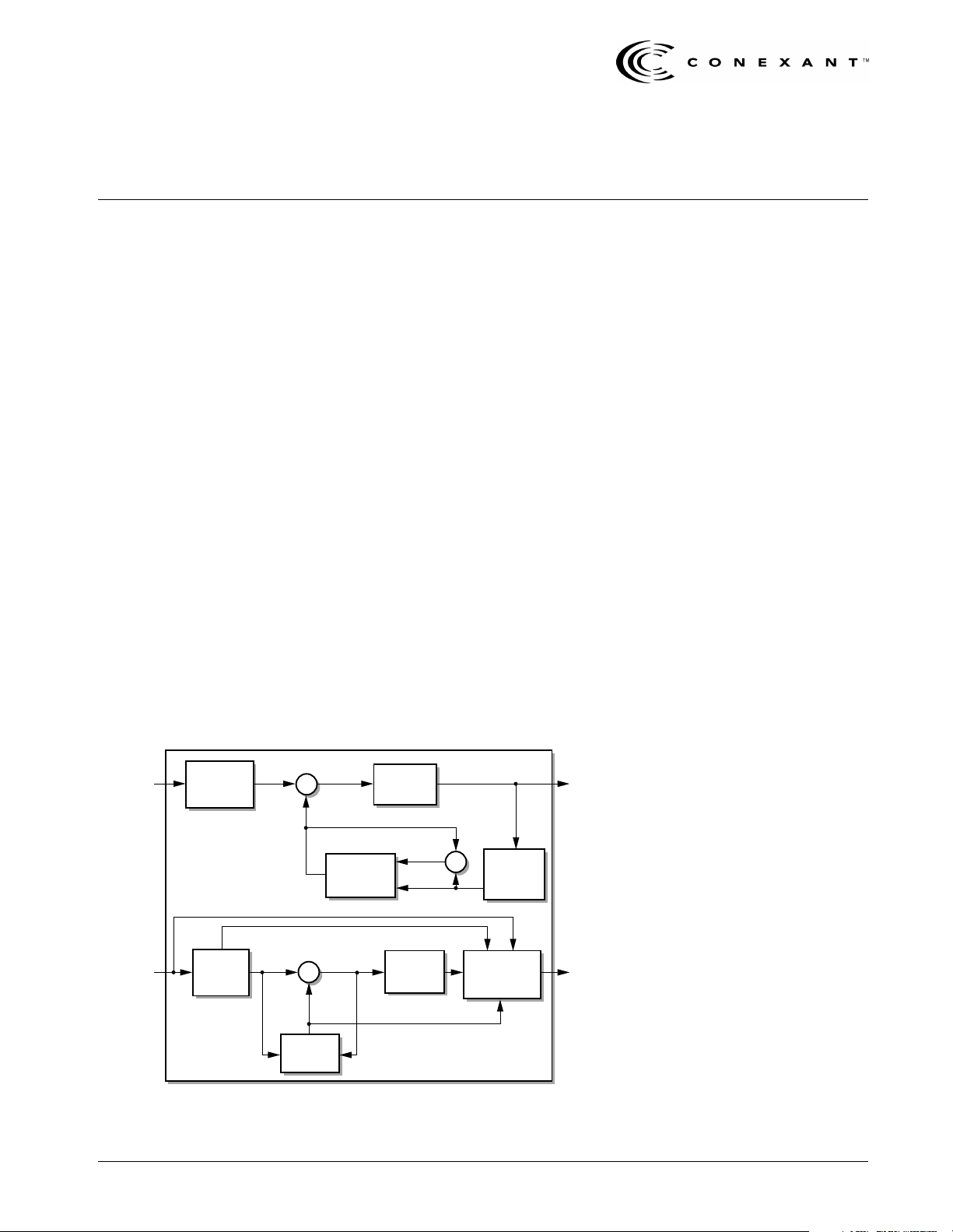
Functional Block Diagram
64 Kbit/s
PCM
Input
32 Kbit/s
ADPCM
Input
Convert to
Uniform
PCM
ENCODER
Inverse
Adaptive
Quantizer
DECODER
Input
Signal
Quantized
Difference
Signal
Difference
+
+
–
Signal
Estimate
Reconstructed
+
+
–
Signal
Estimate
Adaptive
Predictor
Signal
Adaptive
Predictor
Signal
Adaptive
Quantizer
Reconstructed
Signal
Quantized
Difference Signal
Convert to
PCM
+
Quantizer
Synchronous
Coding
Adjustment
32 Kbit/s
ADPCM
Output
Inverse
Adaptive
64 Kbit/s
PCM
Output
Distinguishing Features
• Bt8110B offers internal ROM
• 24 or 32 full-duplex channel capacity
(48 or 64 channels with two
processors)
• 2-, 3-, 4- and 5-bit quantization
dynamically selectable on a
channel-by-channel, frame-by-frame
basis
• Transparent channel operation
• Two control modes available:
microprocessor and hardware.
• Direct framer interface for both T1
and E1 signal formats
• Supports the optimal RESET function
described in the algorithm standards
• Supports even-bit inversion of A-law
inputs and outputs (required by
ITU-T Recommendations G.726, and
G.727)
• Minimum throughput delay
• Pin compatible with Bt8110
• 8 mw per-channel, low-power CMOS
Applicable Standards
• ANSI T1.302-1987
• ANSI T1.303-1989
• ANSI T1.310-1991
• ITU-T G.726, G.727
• ANSI T1.501-1994
• ANSI T1Y1 Technical Reports #3 and
#10
Applications
• T1/E1 Transcoders
• T1/E1 Multiplexers
• Personal Communications Systems:
Digital European Cordless
Telecommunications (DECT),
Personal Access Communications
System (PACS)
• Wireless Local Loop
• Voice PairGain
• DCME Systems
• Speech Processing/Recording
• Voice Mail/Packetization
• Voice over ATM/Frame Relay
Data Sheet 100060C
January 2000
Page 2

Ordering Information
Model Number Package Ambient Temperature Range
Bt8110EPJ 68-Pin Plastic Leaded Chip Carrier (PLCC) –40 °C to +85 °C
Bt8110EPJB 68-Pin Plastic Leaded Chip Carrier (PLCC) –40 °C to +85 °C
Revision History
Revision Level Date Description
A Advanced Created
B December 1996
C January 2000 The timing diagrams for the following figures have been
updated: Figure 2-3, Figure 2-5, Figure 2-6, Figure 2-7,
Figure 2-8, Figure A-2, Figure A-3, Figure A-4.
© 1996, 2000 Conexant Systems, Inc.
All Rights Reserved.
Information in this document is provided in connection with Conexant Systems, Inc. ("Conexant") products. These
materials are provided by Conexant as a service to its customers and may be used for informational purposes only.
Conexant assumes no responsibility for errors or omissions in these materials. Conexant may make changes to
specifications and product descriptions at any time, without notice. Conexant makes no commitment to update the
information contained herein. Conexant shall have no responsibility whatsoever for conflicts or incompatibilities arising
from future changes to its specifications and product descriptions.
No license, express or implied, by estoppel or otherwise, to any intellectual property rights is granted by this document.
Except as provided in Conexant’s Terms and Conditions of Sale for such products, Conexant assumes no liability
whatsoever.
THESE MATERIALS ARE PROVIDED "AS IS" WITHOUT WARRANTY OF ANY KIND, EITHER EXPRESS OR
IMPLIED, RELATING TO SALE AND/OR USE OF CONEXANT PRODUCTS INCLUDING LIABILITY OR WARRANTIES RELATING TO FITNESS FOR A PARTICULAR PURPOSE, MERCHANTABILITY, OR INFRINGEMENT OF ANY
PATENT, COPYRIGHT OR OTHER INTELLECTUAL PROPERTY RIGHT. Conexant further does not warrant the accuracy or completeness of the information, text, graphics or other items contained within these materials. Conexant shall
not be liable for any special, indirect, incidental, or consequential damages, including without limitation, lost revenues
or lost profits, which may result from the use of these materials.
Conexant products are not intended for use in medical, life saving or life sustaining applications. Conexant customers
using or selling Conexant products for use in such applications do so at their own risk and agree to fully indemnify
Conexant for any damages resulting from such improper use or sale.
The following are trademarks of Conexant Systems, Inc.: Conexant, the Conexant C symbol, and “What’s Next in
Communications Technologies”. Product names or services listed in this publication are for identification purposes
only, and may be trademarks of third parties. Third-party brands and names are the property of their respective
owners.
Reader Response: Conexant strives to produce quality documentation and welcomes your feedback. Please send
comments and suggestions to conexant.tech.pubs@conexant.com. For technical questions, contact your local
Conexant sales office or field applications engineer.
100060C Conexant
Page 3

Table of Contents
List of Figures . . . . . . . . . . . . . . . . . . . . . . . . . . . . . . . . . . . . . . . . . . . . . . . . . . . . . . . . . . . . . . . . . . . . . . . . . v
List of Tables . . . . . . . . . . . . . . . . . . . . . . . . . . . . . . . . . . . . . . . . . . . . . . . . . . . . . . . . . . . . . . . . . . . . . . . . . vii
1.0 Product Description. . . . . . . . . . . . . . . . . . . . . . . . . . . . . . . . . . . . . . . . . . . . . . . . . . . . . . . . . . . . . 1-1
1.1 Channel Capacity and Configuration Modes . . . . . . . . . . . . . . . . . . . . . . . . . . . . . . . . . . . . . . . 1-2
1.1.1 Signal Inputs and Outputs . . . . . . . . . . . . . . . . . . . . . . . . . . . . . . . . . . . . . . . . . . . . . . . 1-2
1.1.2 Embedded Coding . . . . . . . . . . . . . . . . . . . . . . . . . . . . . . . . . . . . . . . . . . . . . . . . . . . . . 1-3
1.1.3 Control Mode. . . . . . . . . . . . . . . . . . . . . . . . . . . . . . . . . . . . . . . . . . . . . . . . . . . . . . . . . 1-3
1.2 Pin Descriptions . . . . . . . . . . . . . . . . . . . . . . . . . . . . . . . . . . . . . . . . . . . . . . . . . . . . . . . . . . . . 1-4
2.0 Functional Description . . . . . . . . . . . . . . . . . . . . . . . . . . . . . . . . . . . . . . . . . . . . . . . . . . . . . . . . . . 2-1
2.1 Overview. . . . . . . . . . . . . . . . . . . . . . . . . . . . . . . . . . . . . . . . . . . . . . . . . . . . . . . . . . . . . . . . . . 2-1
2.1.1 Clocking and Synchronization. . . . . . . . . . . . . . . . . . . . . . . . . . . . . . . . . . . . . . . . . . . . . 2-3
2.1.2 Microprocessor Interface . . . . . . . . . . . . . . . . . . . . . . . . . . . . . . . . . . . . . . . . . . . . . . . . 2-3
2.1.3 Address Map . . . . . . . . . . . . . . . . . . . . . . . . . . . . . . . . . . . . . . . . . . . . . . . . . . . . . . . . . 2-4
2.2 Modes of Operation. . . . . . . . . . . . . . . . . . . . . . . . . . . . . . . . . . . . . . . . . . . . . . . . . . . . . . . . . . 2-5
2.2.1 24- or 32-Channel Full-Duplex Interleaved Operation . . . . . . . . . . . . . . . . . . . . . . . . . . . . 2-5
2.2.1.1 Signal Inputs and Outputs . . . . . . . . . . . . . . . . . . . . . . . . . . . . . . . . . . . . . . . 2-6
2.2.1.2 Reset Control . . . . . . . . . . . . . . . . . . . . . . . . . . . . . . . . . . . . . . . . . . . . . . . . 2-8
2.2.2 48- or 64-Channel Encoder-Only Operation . . . . . . . . . . . . . . . . . . . . . . . . . . . . . . . . . . . 2-8
2.2.3 48- or 64-Channel Decoder-Only Operation . . . . . . . . . . . . . . . . . . . . . . . . . . . . . . . . . . . 2-9
2.3 Direct Framer Interface Operation. . . . . . . . . . . . . . . . . . . . . . . . . . . . . . . . . . . . . . . . . . . . . . 2-11
2.3.1 T1 Framer Interface . . . . . . . . . . . . . . . . . . . . . . . . . . . . . . . . . . . . . . . . . . . . . . . . . . . 2-11
2.3.2 E1 Framer Interface . . . . . . . . . . . . . . . . . . . . . . . . . . . . . . . . . . . . . . . . . . . . . . . . . . . 2-12
2.4 Hardware Control . . . . . . . . . . . . . . . . . . . . . . . . . . . . . . . . . . . . . . . . . . . . . . . . . . . . . . . . . . 2-13
2.4.1 Mode Pins . . . . . . . . . . . . . . . . . . . . . . . . . . . . . . . . . . . . . . . . . . . . . . . . . . . . . . . . . . 2-14
2.4.2 Control Pins. . . . . . . . . . . . . . . . . . . . . . . . . . . . . . . . . . . . . . . . . . . . . . . . . . . . . . . . . 2-14
3.0 Registers . . . . . . . . . . . . . . . . . . . . . . . . . . . . . . . . . . . . . . . . . . . . . . . . . . . . . . . . . . . . . . . . . . . . . . 3-1
3.1 0x00–0x3F—Per-Channel Control Registers (per_chan_ctrl). . . . . . . . . . . . . . . . . . . . . . . . . . . 3-1
3.2 0x40—Mode Control Register (mode). . . . . . . . . . . . . . . . . . . . . . . . . . . . . . . . . . . . . . . . . . . . 3-3
100060C Conexant iii
Page 4

Bt8110/8110B
High-Capacity ADPCM Processor
4.0 Electrical and Mechanical Specifications . . . . . . . . . . . . . . . . . . . . . . . . . . . . . . . . . . . . . . . . . 4-1
4.1 Microprocessor Interface Timing. . . . . . . . . . . . . . . . . . . . . . . . . . . . . . . . . . . . . . . . . . . . . . . . 4-1
4.1.1 Bt8110 Timing . . . . . . . . . . . . . . . . . . . . . . . . . . . . . . . . . . . . . . . . . . . . . . . . . . . . . . . . 4-2
4.1.2 ROM Specifications . . . . . . . . . . . . . . . . . . . . . . . . . . . . . . . . . . . . . . . . . . . . . . . . . . . . 4-4
4.2 Absolute Maximum Ratings . . . . . . . . . . . . . . . . . . . . . . . . . . . . . . . . . . . . . . . . . . . . . . . . . . . 4-5
4.3 DC Characteristics . . . . . . . . . . . . . . . . . . . . . . . . . . . . . . . . . . . . . . . . . . . . . . . . . . . . . . . . . . 4-6
4.4 Mechanical Specifications . . . . . . . . . . . . . . . . . . . . . . . . . . . . . . . . . . . . . . . . . . . . . . . . . . . . 4-7
Appendix A. Hardware Mode Operation . . . . . . . . . . . . . . . . . . . . . . . . . . . . . . . . . . . . . . . . . . . . . . . . A-1
A.1 48- or 64-Channel Full-Duplex Hardware Mode Operation . . . . . . . . . . . . . . . . . . . . . . . . . . . . A-1
A.1.1 Introduction. . . . . . . . . . . . . . . . . . . . . . . . . . . . . . . . . . . . . . . . . . . . . . . . . . . . . . . . . A-1
A.1.2 Configuration. . . . . . . . . . . . . . . . . . . . . . . . . . . . . . . . . . . . . . . . . . . . . . . . . . . . . . . . A-1
A.1.3 Functional Timing. . . . . . . . . . . . . . . . . . . . . . . . . . . . . . . . . . . . . . . . . . . . . . . . . . . . . A-3
Appendix B. T1 Speech Compression. . . . . . . . . . . . . . . . . . . . . . . . . . . . . . . . . . . . . . . . . . . . . . . . . . . B-1
B.1 Introduction . . . . . . . . . . . . . . . . . . . . . . . . . . . . . . . . . . . . . . . . . . . . . . . . . . . . . . . . . . . . . . . B-1
B.1.1 Configuration. . . . . . . . . . . . . . . . . . . . . . . . . . . . . . . . . . . . . . . . . . . . . . . . . . . . . . . . B-1
B.1.2 Functional Timing Diagram . . . . . . . . . . . . . . . . . . . . . . . . . . . . . . . . . . . . . . . . . . . . . . B-3
B.1.3 Microprocessor Interface And Per-Channel Configuration . . . . . . . . . . . . . . . . . . . . . . . B-5
Appendix C. E1 Speech Compression. . . . . . . . . . . . . . . . . . . . . . . . . . . . . . . . . . . . . . . . . . . . . . . . . . . C-1
C.1 Introduction . . . . . . . . . . . . . . . . . . . . . . . . . . . . . . . . . . . . . . . . . . . . . . . . . . . . . . . . . . . . . . . C-1
C.1.1 Configuration. . . . . . . . . . . . . . . . . . . . . . . . . . . . . . . . . . . . . . . . . . . . . . . . . . . . . . . . C-1
C.1.2 Functional Timing Diagram . . . . . . . . . . . . . . . . . . . . . . . . . . . . . . . . . . . . . . . . . . . . . . C-3
C.1.3 Microprocessor Interface and Per-Channel Configuration. . . . . . . . . . . . . . . . . . . . . . . . C-5
Appendix D. T1 ADPCM Transcoder . . . . . . . . . . . . . . . . . . . . . . . . . . . . . . . . . . . . . . . . . . . . . . . . . . . . D-1
D.1 Introduction . . . . . . . . . . . . . . . . . . . . . . . . . . . . . . . . . . . . . . . . . . . . . . . . . . . . . . . . . . . . . . . D-1
D.1.1 Description . . . . . . . . . . . . . . . . . . . . . . . . . . . . . . . . . . . . . . . . . . . . . . . . . . . . . . . . . D-1
D.1.2 Summary. . . . . . . . . . . . . . . . . . . . . . . . . . . . . . . . . . . . . . . . . . . . . . . . . . . . . . . . . . . D-3
D.1.3 ADPCM Transcoder System Specifications . . . . . . . . . . . . . . . . . . . . . . . . . . . . . . . . . . D-4
Appendix E. E1 ADPCM Transcoder . . . . . . . . . . . . . . . . . . . . . . . . . . . . . . . . . . . . . . . . . . . . . . . . . . . . . E-1
E.1 Introduction . . . . . . . . . . . . . . . . . . . . . . . . . . . . . . . . . . . . . . . . . . . . . . . . . . . . . . . . . . . . . . . E-1
E.1.1 Description . . . . . . . . . . . . . . . . . . . . . . . . . . . . . . . . . . . . . . . . . . . . . . . . . . . . . . . . . . E-1
E.1.2 Summary. . . . . . . . . . . . . . . . . . . . . . . . . . . . . . . . . . . . . . . . . . . . . . . . . . . . . . . . . . . . E-3
E.1.3 ADPCM Transcoder System Specifications . . . . . . . . . . . . . . . . . . . . . . . . . . . . . . . . . . . E-3
iv Conexant 100060C
Page 5

Bt8110/8110B List of Figures
High-Capacity ADPCM Processor
List of Figures
Figure 1-1. Bt8110 Pinout Diagram . . . . . . . . . . . . . . . . . . . . . . . . . . . . . . . . . . . . . . . . . . . . . . . . . . . . 1-4
Figure 1-2. Bt8110 Logic Diagram. . . . . . . . . . . . . . . . . . . . . . . . . . . . . . . . . . . . . . . . . . . . . . . . . . . . . 1-6
Figure 1-3. Bt8110B Pinout Diagram. . . . . . . . . . . . . . . . . . . . . . . . . . . . . . . . . . . . . . . . . . . . . . . . . . . 1-7
Figure 1-4. Bt8110B Logic Diagram . . . . . . . . . . . . . . . . . . . . . . . . . . . . . . . . . . . . . . . . . . . . . . . . . . . 1-9
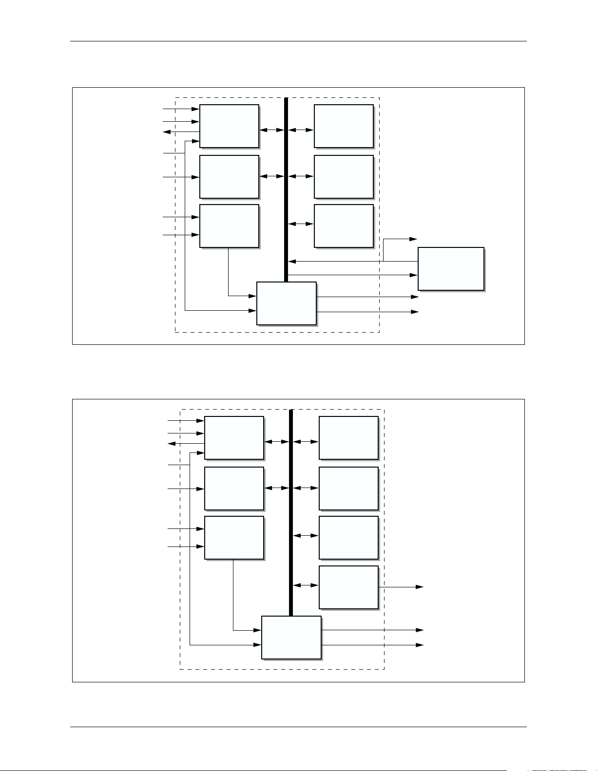
Figure 2-1. Bt8110 Block Diagram. . . . . . . . . . . . . . . . . . . . . . . . . . . . . . . . . . . . . . . . . . . . . . . . . . . . . 2-2
Figure 2-2. Bt8110B Block Diagram . . . . . . . . . . . . . . . . . . . . . . . . . . . . . . . . . . . . . . . . . . . . . . . . . . . 2-2
Figure 2-3. Input and Output Timing for 24- or 32-Channel Full-Duplex
Interleaved Operation (Microprocessor Control) . . . . . . . . . . . . . . . . . . . . . . . . . . . . . . . . . 2-6
Figure 2-4. Input and Output Timing for 48- or 64-Channel Half-Duplex
Encoder-Only Operation (Microprocessor Control) . . . . . . . . . . . . . . . . . . . . . . . . . . . . . . . 2-9
Figure 2-5. Input and Output Timing for 48- or 64-Channel Half-Duplex
Decoder-Only Operation (Microprocessor Control). . . . . . . . . . . . . . . . . . . . . . . . . . . . . . 2-10
Figure 2-6. Hardware Control Interleaved Timing . . . . . . . . . . . . . . . . . . . . . . . . . . . . . . . . . . . . . . . . 2-15
Figure 2-7. Hardware Control Encoder-Only Timing . . . . . . . . . . . . . . . . . . . . . . . . . . . . . . . . . . . . . . 2-16
Figure 2-8. Hardware Control Decoder-Only Timing . . . . . . . . . . . . . . . . . . . . . . . . . . . . . . . . . . . . . . 2-17
Figure 4-1. Microprocessor Interface Timing . . . . . . . . . . . . . . . . . . . . . . . . . . . . . . . . . . . . . . . . . . . . 4-2
Figure 4-2. Input and Output Signal Timing. . . . . . . . . . . . . . . . . . . . . . . . . . . . . . . . . . . . . . . . . . . . . . 4-3
Figure 4-3. 68-Pin Plastic Leaded Chip Carrier (J-Bend). . . . . . . . . . . . . . . . . . . . . . . . . . . . . . . . . . . . 4-7
Figure A-1. 48- or 64-Channel Configuration of the Bt8110/8110B. . . . . . . . . . . . . . . . . . . . . . . . . . . . A-2
Figure A-2. 48- or 64-Channel Full-Duplex Interleaved Mode Functional Timing . . . . . . . . . . . . . . . . . . A-3
Figure A-3. 96- or 128-Channel Half-Duplex Encoder-Only Functional Timing. . . . . . . . . . . . . . . . . . . . A-4
Figure A-4. 96- or 128-Channel Half-Duplex Decoder-Only Functional Timing . . . . . . . . . . . . . . . . . . . A-5
Figure B-1. T1 Speech Compression Interface Block Diagram. . . . . . . . . . . . . . . . . . . . . . . . . . . . . . . . B-2
Figure B-2. T1 Speech Compression Functional Timing Diagram . . . . . . . . . . . . . . . . . . . . . . . . . . . . . B-4
Figure C-1. E1 Speech Compression Interface Configuration . . . . . . . . . . . . . . . . . . . . . . . . . . . . . . . . C-2
Figure C-2. E1 Speech Compression Functional Timing Diagram . . . . . . . . . . . . . . . . . . . . . . . . . . . . . C-4
Figure D-1. Single-Board Transcoder Assembly. . . . . . . . . . . . . . . . . . . . . . . . . . . . . . . . . . . . . . . . . . .D-2
Figure D-2. Single-Board Transcoder Application . . . . . . . . . . . . . . . . . . . . . . . . . . . . . . . . . . . . . . . . .D-3
Figure E-1. Single-Board Transcoder Assembly. . . . . . . . . . . . . . . . . . . . . . . . . . . . . . . . . . . . . . . . . . .E-2
Figure E-2. Single-Board Transcoder Application . . . . . . . . . . . . . . . . . . . . . . . . . . . . . . . . . . . . . . . . .E-3
100060C Conexant v
Page 6

List of Figures Bt8110/8110B
High-Capacity ADPCM Processor
vi Conexant 100060C
Page 7

Bt8110/8110B List of Tables
High-Capacity ADPCM Processor
List of Tables
Table 1-1. ADPCM Operational Modes. . . . . . . . . . . . . . . . . . . . . . . . . . . . . . . . . . . . . . . . . . . . . . . . . . 1-2
Table 1-2. Bt8110 Pin Descriptions . . . . . . . . . . . . . . . . . . . . . . . . . . . . . . . . . . . . . . . . . . . . . . . . . . . . 1-5
Table 1-3. Bt8110B Pin Descriptions . . . . . . . . . . . . . . . . . . . . . . . . . . . . . . . . . . . . . . . . . . . . . . . . . . . 1-8
Table 1-4. Bt8110/8110B Hardware Signal Definitions . . . . . . . . . . . . . . . . . . . . . . . . . . . . . . . . . . . . 1-10
Table 2-1. Signal Connections . . . . . . . . . . . . . . . . . . . . . . . . . . . . . . . . . . . . . . . . . . . . . . . . . . . . . . . . 2-4
Table 2-2. Parallel Signal Input Bus . . . . . . . . . . . . . . . . . . . . . . . . . . . . . . . . . . . . . . . . . . . . . . . . . . . . 2-7
Table 2-3. Parallel Signal Output Bus. . . . . . . . . . . . . . . . . . . . . . . . . . . . . . . . . . . . . . . . . . . . . . . . . . . 2-8
Table 2-4. Bt8110/8110B Connection for Hardware Mode. . . . . . . . . . . . . . . . . . . . . . . . . . . . . . . . . . 2-13
Table 2-5. Mode Pins . . . . . . . . . . . . . . . . . . . . . . . . . . . . . . . . . . . . . . . . . . . . . . . . . . . . . . . . . . . . . . 2-14
Table 3-1. Bt8110 or Bt8110B with External Lookup Table ROM . . . . . . . . . . . . . . . . . . . . . . . . . . . . . . 3-2
Table 3-2. Bt8110B Internal Lookup Table ROM . . . . . . . . . . . . . . . . . . . . . . . . . . . . . . . . . . . . . . . . . . 3-2
Table 3-3. Interleaved Operation . . . . . . . . . . . . . . . . . . . . . . . . . . . . . . . . . . . . . . . . . . . . . . . . . . . . . . 3-5
Table 3-4. Encoder/Decoder–Only Operation . . . . . . . . . . . . . . . . . . . . . . . . . . . . . . . . . . . . . . . . . . . . . 3-6
Table 4-1. Microprocessor Interface Timing . . . . . . . . . . . . . . . . . . . . . . . . . . . . . . . . . . . . . . . . . . . . . 4-1
Table 4-2. Bt8110/8110B Hardware Mode Timing . . . . . . . . . . . . . . . . . . . . . . . . . . . . . . . . . . . . . . . . . 4-3
Table 4-3. Input and Output Signal Timing. . . . . . . . . . . . . . . . . . . . . . . . . . . . . . . . . . . . . . . . . . . . . . . 4-3
Table 4-4. System Clock Frequencies . . . . . . . . . . . . . . . . . . . . . . . . . . . . . . . . . . . . . . . . . . . . . . . . . . 4-4
Table 4-5. Absolute Maximum Ratings . . . . . . . . . . . . . . . . . . . . . . . . . . . . . . . . . . . . . . . . . . . . . . . . . 4-5
Table 4-6. DC Characteristics. . . . . . . . . . . . . . . . . . . . . . . . . . . . . . . . . . . . . . . . . . . . . . . . . . . . . . . . . 4-6
Table A-1. Mode Settings. . . . . . . . . . . . . . . . . . . . . . . . . . . . . . . . . . . . . . . . . . . . . . . . . . . . . . . . . . . . A-2
Table B-1. Bt8110/8110B Microprocessor Connection . . . . . . . . . . . . . . . . . . . . . . . . . . . . . . . . . . . . . B-5
Table B-2. Microcontroller Memory Map . . . . . . . . . . . . . . . . . . . . . . . . . . . . . . . . . . . . . . . . . . . . . . . . B-6
Table B-3. Bt8110/8110B Processor Per-Channel Control Locations. . . . . . . . . . . . . . . . . . . . . . . . . . . B-7
Table C-1. Bt8110/8110B Microprocessor Connection . . . . . . . . . . . . . . . . . . . . . . . . . . . . . . . . . . . . . C-5
Table C-2. Bt8110/8110B Microprocessor Memory Map. . . . . . . . . . . . . . . . . . . . . . . . . . . . . . . . . . . . C-6
Table C-3. Bt8110/B Per-Channel Control Locations . . . . . . . . . . . . . . . . . . . . . . . . . . . . . . . . . . . . . . . C-7
Table D-1. ADPCM Transcoder System Specifications . . . . . . . . . . . . . . . . . . . . . . . . . . . . . . . . . . . . . . D-4
Table E-1. ADPCM Transcoder System Specifications . . . . . . . . . . . . . . . . . . . . . . . . . . . . . . . . . . . . . . E-3
100060C Conexant vii
Page 8

List of Tables Bt8110/8110B
High-Capacity ADPCM Processor
viii Conexant 100060C
Page 9

1
1.0 Product Description
The Adaptive Differential Pulse Code Modulation (ADPCM) algorithm is a
transcoding operation which consists of encoding 64 kbit/s Pulse Code
Modulation (PCM) to 16, 24, 32, or 40 kbit/s ADPCM and decoding from
ADPCM to 64 kbit/s PCM. The multichannel processor provides transcoding for
both A-law and
channel-by-channel basis.
The Bt8110/8110B has a maximum capacity of 64 channels of ADPCM
operations. It can be configured to provide 24 or 32 full-duplex channels
providing both encoding and decoding. It can also be configured to provide 48 or
64 half-duplex channels providing either encoding or decoding. The
Bt8110/8110B consists of a VLSI CMOS integrated circuit and a ROM.
NOTE: In the Bt8110, the ROM is external. Additionally, for the Bt8110, a 64 K
ROM will provide six different ADPCM codes, while a 128 K ROM will
provide 14 different ADPCM codes. (See Table 3-1.). The Bt8110B has an
internal ROM or can be used with the external ROM. The Bt8110B’s
internal ROM contains 14 different ADPCM codes (see Tabl e 3- 2),
µ-law PCM codes. The PCM coding rate is selectable on a
Two Bt8110/8110Bs and a single ROM can be configured to provide 48 or 64
full-duplex channels for operation in transcoding applications. There are two
control modes for the Bt8110/8110B: Hardware and Microprocessor. The
hardware mode provides for input of code selection, transparency selection,
algorithm reset, and PCM coding law on a per-channel basis. The microprocessor
mode is provided via an integral interface to a microprocessor consisting of a
microprocessor, program and data memory, and desired status indicators.
100060C Conexant 1-1
Page 10

1.0 Product Description Bt8110/8110B
1.1 Channel Capacity and Configuration Modes High-Capacity ADPCM Processor
1.1 Channel Capacity and Configuration Modes
There are four configurations for the operational mode of the Bt8110/8110B (see
Table 1 -1 ). These configurations are established by setting the three mode control
bits ([MODE[2:0]) and the enable framer bit [EN_FRMR] in the Mode Control
Register [mode; 0x40], in the microprocessor mode or on signal pins in the
hardware mode (AD[2:0] and CTRL[0]). Table 1-1 summarizes the
configurations and the input code applied to each.
Table 1-1. ADPCM Operational Modes
CTRL
[1]
NOTE(S):
(1)
2. CTRL[1] and CTRL[0] are available only in the Bt8110B.
CTRL
[0]
x0100
x 0 101 Encoder Only 6.144 48
x 0 110 Decoder Only 6.144 48
0 1 100 Direct Framer Interface 12.352 24
Interleaved operation means that the Bt8110/8110B alternates between encoder and decoder operation on consecutive
inputs. This requires that the inputs and outputs be interleaved (PCM/ADPCM/PCM, etc.) as well.
Mode
Control
Function
Encoder/Decoder Interleaved
In T1 and E1 direct framer interface modes the Bt8110/8110B can connect
directly to a T1 or E1 framer providing 24 or 32 full-duplex channels of encoding.
These configurations are described in detail in Appendix B and C.
(1)
Clock
Rate
(MHz)
6.144 24
Channel
Capacity
Full-duplex
Half-duplex
Half-duplex
Full-duplex
Clock
Rate
(MHz)
8.192 32 Full-duplex
8.192 64 Half-duplex
8.192 64 Half-duplex
8.192 32 Full-duplex
1.1.1 Signal Inputs and Outputs
Channel
Capacity
The Bt8110/8110B provides both parallel and serial inputs and outputs. The 8-bit
parallel inputs are selected by setting the input PSIGEN high. The serial input is a
multiplexed encoder/decoder input to provide interleaved signals. The transfer
rate of the serial input and output is one-half the input clock rate (CLOCK). The
serial output is also multiplexed in interleaved encoder/decoder operation.
ADPCM inputs and outputs appear on the most significant bits.
The serial signal input and output words are 8 bits, with the most signif icant
bit (sign bit for PCM) appearing first. When transparent operation is selected for
a given channel for either an encoder or a decoder, all 8 bits are transferred
without modification from the input to both the serial and parallel outputs.
NOTE: The exception is with the Bt8110 when the parallel interface is selected in
the direct T1/E1 framer interface mode; then the decoder path PSIG[0]
must held at a logic low level.
1-2 Conexant 100060C
Page 11

Bt8110/8110B 1.0 Product Description
High-Capacity ADPCM Processor
1.1.2 Embedded Coding
The Bt8110/8110B has the capability to provide embedded coding according to
ANSI Standard T1.310-1991 and ITU-T Recommendation G.727. This coding
technique allows the encoding to be performed with 5 bits of encoding
information, and the decoding to be done with anywhere from 2 to 5 input bits.
The coding algorithm is defined so that although the coding distortion increases
as the number of bits at the decoder decreases, the encoder and the decoder will
remain synchronized.
ROM code selected. Along with four different standard (non-embedded) ADPCM
codes, two embedded codes can be provided with a 64 K ROM and up to six
different embedded codes, with eight different standard (non-embedded) codes,
can be provided with a 128 K ROM. The encoder always provides the maximum
number of bits (up to 5) defined by the code selected. The decoder requires up to
5 ADPCM bits and a 2-bit encoded input that indicates how many bits are present
at the decoder input. This input signal is applied to bits 1 and 2 of the parallel
input bus. If embedded coding is not in use, bits 1 and 2 should be connected to
ground.
1.1.3 Control Mode
1.1 Channel Capacity and Configuration Modes
The Bt8110/8110B is designed so that embedded coding is enabled by the
Each channel has four sets of per-channel control inputs. These are for selecting
the PCM coding law (A-law or
the RESET function of the ADPCM coding algorithm, and selecting which of 14
codes (six codes for a 64 K ROM) is used for encoding or decoding.
The microprocessor mode is selected by setting input MICREN high. The
microprocessor can address 65 different registers. There is a control register for
each of the encoder and decoder channel operations and a mode control register
that sets the operating mode of the Bt8110/8110B.
µ-law), selecting transparent operation, selecting
100060C Conexant 1-3
Page 12
1.0 Product Description Bt8110/8110B
1.2 Pin Descriptions High-Capacity ADPCM Processor
1.2 Pin Descriptions
The Bt8110 and Bt8110B are packaged as 68-pin Plastic Leaded Chip Carriers
(PLCCs). Figures 1-1 and 1-2 illustrate the pinouts for the Bt8110 and Bt8110B,
respectively. Pin assignments are listed in numerical order in Table 1 -2 for
Bt8110, and in Tab le 1 -3 for Bt8110B. Figures 1-2 and 1-4 show the functionally
partitioned logic diagrams for Bt8110 and Bt8110B. Pin descriptions, names, and
I/O assignments are detailed in Table 1-2.
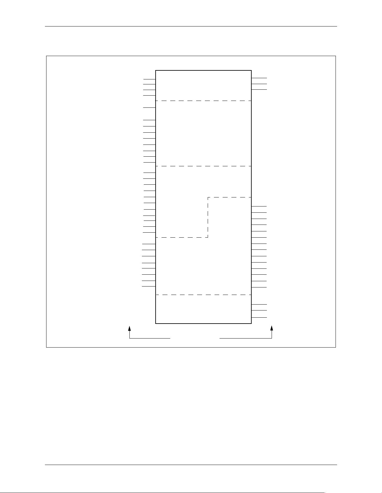
Figure 1-1. Bt8110 Pinout Diagram
VCC
PSIGEN
PSIG[7]
PSIG[6]
PSIG[5]
PSIG[4]
WR*
PSIG[3]
GND
VCC
PSIG[2]
PSIG[1]
PSIG[0]
GND
A[0]
A[1]
A[2]
GND
AD[0]
AD[1]
AD[2]
SERIAL_IN
CLOCK
SERIAL_OUT
VCC
GND
AD[3]
RESET
SYNC
CS
MICREN
AD[4]
AD[5]
VCC
987654321
10
11
12
13
14
15
16
17
18
19
20
21
22
23
24
25
26
2728293031323334353637383940414243
GND
ALE
AD[6]
Processor
Y
TDP
PCM_STB
ADPCM_STB
68676665646362
Bt8110
ADPCM
SE
VCC
GND
A[13]
AD[12]
VCC
GND
AD[11]
AD[10]
61
60
59
58
57
56
55
54
53
52
51
50
49
48
47
46
45
44
A[9]
A[3]
A[4]
A[5]
D[0]
D[1]
D[2]
D[3]
VCC
GND
D[4]
D[5]
D[6]
D[7]
A[6]
A[7]
A[8]
GND
100060_002
1-4 Conexant 100060C
Page 13

Bt8110/8110B 1.0 Product Description
High-Capacity ADPCM Processor
Table 1-2. Bt8110 Pin Descriptions
1.2 Pin Descriptions
Pin Pin Label I/O Pin Pin Label I/O
1 GND I 35 GND I
2 PSIG[3] I 36 VCC I
3WR*I37A[13]O
4 PSIG[4] I 38 A[12] O
5 PSIG[5] I 39 VCC I
6 PSIG[6] I 40 GND I
7 PSIG[7] (MSB) I 41 A[11] O
8 PSIGEN I 42 A[10] O
9VCCI43A[9]O
10 GND I 44 GND I
11 AD[0] I 45 A[8] O
12 AD[1] I 46 A[7] O
13 AD[2] I 47 A[6] O
14 SERIAL_IN I 48 D[7] I
15 CLOCK I 49 D[6] I
16 SERIAL_OUT O 50 D[5] I
17 VCC I 51 D[4] I
18 GND I 52 GND I
19 AD[3] I 53 VCC I
20 RESET I 54 D[3] I
21 SYNC I 55 D[2] I
22 CS I 56 D[1] I
23 MICREN I 57 D[0] I
24 AD[4] I 58 A[5] 0
25 AD[5] I 59 A[4] O
26 VCC I 60 A[3] O
27 GND I 61 A[2] O
28 AD[6] I 62 A[1] O
29 ALE I 63 A[0] O
30 PCM_STB O 64 GND I
31 ADPCM_STB O 65 PSIG[0] I
32 Y O 66 PSIG[1] I
33 TDP O 67 PSIG[2] I
34 SE O 68 VCC I
100060C Conexant 1-5
Page 14
1.0 Product Description Bt8110/8110B
1.2 Pin Descriptions High-Capacity ADPCM Processor
Figure 1-2. Bt8110 Logic Diagram
Clock In
Sync In
Serial Input
Parallel Signal Enable
(MSB) Parallel Signal In 7
Parallel Signal In 6
Parallel Signal In 5
Parallel Signal In 4
Parallel Signal In 3
Parallel Signal In 2 I PSIG[2]
Parallel Signal In 1
Parallel Signal In 0
Microcontroller Enable
Address Latch Enable
Chip Select
µP Address/Data 6
µP Address/Data 5
µP Address/Data 4
µP Address/Data 1 I AD[1]
µP Address/Data 0
ROM Data 7
ROM Data 6
ROM Data 5
ROM Data 4
ROM Data 3
ROM Data 2
ROM Data 1
ROM Data 0 I
Reset
Write*
I
I
I
I
I
I
I
I
I
I
I
I
I
I
I
I
I
I
I
IµP Address/Data 3
I
I
I
I
I
I
I
I
15
21
14
20
8
7
6
5
4
2
67
66
65
23
29
22
3
28
25
24
19
13
12
11
48
49
50
51
54
55
56
57
CLOCK
SYNC
SERIAL_IN
RESET
PSIGEN
PSIG[7]
PSIG[6]
PSIG[5]
PSIG[4]
PSIG[3]
PSIG[1]
PSIG[0]
MICREN
ALE
CS
WR*
AD[6]
AD[5]
AD[4]
AD[3]
AD[2]IµP Address/Data 2
AD[0]
D[7]
D[6]
D[5]
D[4]
D[3]
D[2]
D[1]
D[0]
Clock and
Serial
Interface
Parallel Input Interface
Microprocessor
SERIAL_OUT
Interface
ROM
Interface
ADPCM_STB
PCM_STB
A[13]
A[12]
A[11]
A[10]
A[9]
A[8]
A[7]
A[6]
A[5]
A[4]
A[3]
A[2]
A[1]
A[0]
31
30
16
37
38
41
42
43
45
46
47
58
59
60
61
62
63
ADPCM Strobe
O
PCM Strobe
O
Serial Output
O
ROM Address 13
O
ROM Address 12
O
ROM Address 11
O
ROM Address 10
O
ROM Address 9
O
ROM Address 8
O
ROM Address 7
O
ROM Address 6
O
ROM Address 5
O
ROM Address 4
O
ROM Address 3
O
ROM Address 2
O
ROM Address 1
O
ROM Address 0
O
Test
Interface
I = Input, O = Output
34
33
TDP TDP ParameterO
Y O Y Parameter
32
SE Parameter
O
100060_003
SE
1-6 Conexant 100060C
Page 15

Bt8110/8110B 1.0 Product Description
High-Capacity ADPCM Processor
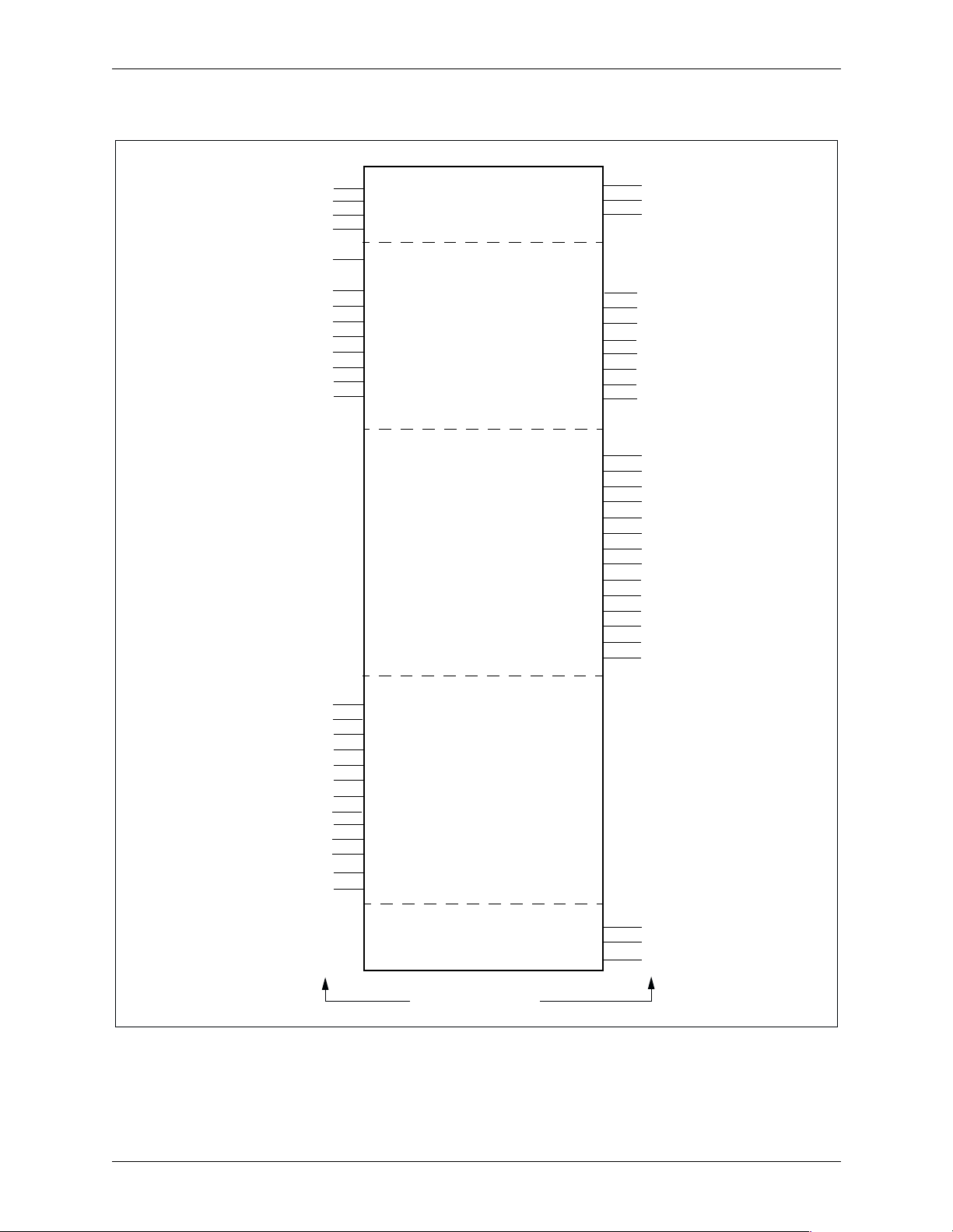
Figure 1-3. Bt8110B Pinout Diagram
GND
AD[0]
AD[1]
AD[2]
SERIAL_IN
CLOCK
SERIAL_OUT
VCC
GND
AD[3]
RESET
SYNC
CS
MICREN
AD[4]
AD[5]
VCC
VCC
PSIGEN
PSIG[7]
PSIG[6]
PSIG[5]
PSIG[4]
WR*
PSIG[3]
GND
VCC
PSIG[2]
PSIG[1]
PSIG[0]
GND
987654321
10
11
12
13
14
15
16
17
18
19
20
21
22
23
24
25
26
2728293031323334353637383940414243
ALE
GND
AD[6]
Processor
Y
TDP
PCM_STB
ADPCM_STB
68676665646362
Bt8110B
ADPCM
SE
VCC
GND
A[13]
A[12]
CTRL[1]
CTRL[0]
1.2 Pin Descriptions
A[0]
A[1]
A[2]
61
A[3]
60
A[4]
59
A[5]
58
D[0]
57
D[1]
56
D[2]
55
D[3]
54
VCC
53
GND
52
D[4]
51
D[5]
50
D[6]
49
D[7]
48
A[6]
47
A[7]
46
A[8]
45
44
GND
A[9]
A[11]
A[10]
100060_004
100060C Conexant 1-7
Page 16

1.0 Product Description Bt8110/8110B
1.2 Pin Descriptions High-Capacity ADPCM Processor
Table 1-3. Bt8110B Pin Descriptions
Pin Pin Label I/O Pin Pin Label I/O
1 GND I 35 GND I
2 PSIG[3] I 36 VCC I
3WR*I37A[13]O
4 PSIG[4] I 38 A[12] O
5 PSIG[5] I 39 CTRL[1] I
6 PSIG[6] I 40 CTRL[0] I
7 PSIG[7] (MSB) I 41 A[11] O
8PSIGEN I42 A[10] O
9VCCI43A[9]O
10 GND I 44 GND I
11 AD[0] I 45 A[8] O
12 AD[1] I 46 A[7] I/O
13 AD[2] I 47 A[6] I/O
14 SERIAL_IN I 48 D[7] I
15 CLOCK I 49 D[6] I
16 SERIAL_OUT O 50 D[5] I
17 VCC I 51 D[4] I
18 GND I 52 GND I
19 AD[3] I 53 VCC I
20 RESET I 54 D[3] I
21 SYNC I 55 D[2] I
22 CS I 56 D[1] I
23 MICREN I 57 D[0] I
24 AD[4] I 58 A[5] I/0
25 AD[5] I 59 A[4] I/O
26 VCC I 60 A[3] I/O
27 GND I 61 A[2] I/O
28 AD[6] I 62 A[1] I/O
29 ALE I 63 A[0] I/O
30 PCM_STB O 64 GND I
31 ADPCM_STB O 65 PSIG[0] I
32 Y O 66 PSIG[1] I
33 TDP O 67 PSIG[2] I
34 SE O 68 VCC I
1-8 Conexant 100060C
Page 17
Bt8110/8110B 1.0 Product Description
High-Capacity ADPCM Processor
Figure 1-4. Bt8110B Logic Diagram
Clock In
Sync In
Serial Input
Reset
Parallel Signal Enable
(MSB) Parallel Signal In 7
Parallel Signal In 6
Parallel Signal In 5
Parallel Signal In 4
Parallel Signal In 3
Parallel Signal In 2 I PSIG[2]
Parallel Signal In 1
Parallel Signal In 0
1.2 Pin Descriptions
D[7]
D[6]
D[5]
D[4]
D[3]
D[2]
D[1]
D[0]
A[13]
A[12]
A[11]
A[10]
A[9]
A[8]
A[7]
A[6]
A[5]
A[4]
A[3]
A[2]
A[1]
A[0]
31
30
16
48
49
50
51
54
55
56
57
37
38
41
42
43
45
46
47
58
59
60
61
62
63
ADPCM Strobe
O
PCM Strobe
O
Serial Output
O
ROM Data In/PData Out
I/O
ROM Data In/PData Out
I/O
ROM Data In/PData Out
I/O
ROM Data In/PData Out
I/O
ROM Data In/PData Out
I/O
ROM Data In/PData Out
I/O
ROM Data In/PData Out
I/O
ROM Data In/PData Out
I/O
ROM Address 13
O
ROM Address 12
O
ROM Address 11
O
ROM Address 10
O
ROM Address 9
O
ROM Address 8
O
ROM Address 7
I/O
ROM Address 6
I/O
ROM Address 5
I/O
ROM Address 4
I/O
ROM Address 3
I/O
ROM Address 2
I/O
ROM Address 1
I/O
ROM Address 0
I/O
15
I
I
I
I
I
I
I
I
I
I
I
I
21
14
20
8
7
6
5
4
2
67
66
65
CLOCK
SYNC
SERIAL_IN
RESET
PSIGEN
PSIG[7]
PSIG[6]
PSIG[5]
PSIG[4]
PSIG[3]
PSIG[1]
PSIG[0]
Clock and
Serial
Interface
Parallel
Interface
(ROM Interface)
ROM
Interface
ADPCM_STB
SERIAL_OUT
PCM_STB
Microcontroller Enable
Address Latch Enable
Chip Select
Write*
µP Address/Data 6
µP Address/Data 5
µP Address/Data 4
µP Address/Data 1 I AD[1]
µP Address/Data 0
Control Inputs
Control Inputs
23
I
29
I
22
I
3
I
28
I
25
I
24
I
19
IµP Address/Data 3
13
12
11
I
I
39
40
I
MICREN
ALE
CS
WR*
AD[6]
AD[5]
AD[4]
AD[3]
AD[2]IµP Address/Data 2
AD[0]
CTRL[1]
CTRL[0]
I = Input, O = Output
Microprocessor and
Hardware Control
Interface
Test
Interface
SE
34
33
TDP TDP ParameterO
Y O Y Parameter
32
SE Parameter
O
100060_005
100060C Conexant 1-9
Page 18

1.0 Product Description Bt8110/8110B
1.2 Pin Descriptions High-Capacity ADPCM Processor
Table 1-4. Bt8110/8110B Hardware Signal Definitions (1 of 2)
Pin Label Signal Name I/O Definition
CLOCK Clock I The system clock provided to the Bt8110/8110B. Maximum clock
frequency is 16.5 MHz, and it must have minimum high and low
periods of 27 ns (duty cycle of 45% to 55% at 16.5 MHz, or 22%
to 78% at 8.192 MHz).
SYNC Synchronization I Provides input and output synchronization.
(1)
RESET
ADPCM_STB ADPCM Strobe O Active when the parallel ADPCM inputs and outputs are enabled in
PCM_STB PCM Strobe O Active when the parallel PCM inputs and outputs are enabled in
Clock I and Serial Interface
SERIAL_IN Serial Data Input I This pin has multiplexed PCM and ADPCM signals in interleaved
Reset I Selects the algorithm reset function per ANSI T1.303-1989 and
ITU-T G.726.
interleaved mode, and is active for both PCM inputs and ADPCM
outputs in encoder mode. This pin is disabled in decoder mode.
interleaved mode, and is active for both ADPCM inputs and PCM
outputs in decoder mode. This pin is disabled in encoder mode.
mode; PCM signals for encoder mode, and ADPCM signals for
decoder mode.
SERIAL_OUT Serial Data Output O This pin has multiplexed PCM and ADPCM signals in interleaved
mode; ADPCM signals for encoder mode, and PCM signals for
decoder mode.
PSIGEN Parallel Signal Enable I A control signal that enables parallel inputs. Does not affect parallel
outputs (D[7:0]), which are always available. On the Bt8110B, this
signal has extra functionality (see note in Section 2.2.1.1).
PSIG[7:0] Parallel Signal Input I The parallel input data bus. The most significant bit (sign bit for
PCM, I1 for ADPCM) appears on PSIG[7]. This input bus is also
used to indicate ADPCM word length when embedded decoding is
performed. When serial inputs are used, these inputs should be left
unconnected (internal pull-down resistors included) except as
required for embedded decoding.
Parallel Interface
D[7:0] Parallel Signal Output/
ROM Data Input
Microprocessor Interface
MICREN
(1)
CS
(1)
WR*
(1)
ALE
(1)
Microprocessor Enable I Active high input that selects per-channel control via a
Chip Select I Active high input that enables write operations to the
Write* I Active low input that performs the write operation to the
µP Address Latch
Enable.
I/O On the Bt8110, these signals are inputs, accepting data from the
external lookup table ROM. The data on these pins also provides
parallel PCM and ADPCM output functionality for the Bt8110. On
the Bt8110B, these signals are outputs when internal ROM is used.
D[7] is the most significant bit of the PCM and ADPCM data.
microprocessor interface.
Bt8110/8110B. In hardware mode this pin enables transparent
operation.
Bt8110/8110B. In hardware mode this pin enables A-law PCM
coding (low for µ-law).
I ALE is a microprocessor-generated signal that causes the
Bt8110/8110B to latch in the address on the address/data bus. ALE
is active high with the address being latched on the falling edge of
the signal. In hardware mode this pin becomes an optional code
input.
AD[6:0] µP Address/Data Bus I Microprocessor 7-bit address and data bus.
1-10 Conexant 100060C
Page 19

Bt8110/8110B 1.0 Product Description
High-Capacity ADPCM Processor
Table 1-4. Bt8110/8110B Hardware Signal Definitions (2 of 2)
Pin Label Signal Name I/O Definition
A[13:0] ROM Address Bus I/O On the Bt8110, these signals are ouputs driving the address lines
on the external lookup table ROM. On the Bt8110B, A[7:0] are
inputs when internal lookup table ROM is used. A[13:8] must be
left open when using the Bt8110B with internal lookup table ROM
enabled.
using Bt8110B with internal lookup table ROM enabled.
enabled, A[0] and A[3] have the following functions:
• A[0] Disable G.726 TR predictor reset. This function forces the
• A[3] Disable even-bit inversion in A-law. This function disables
• A[2:0], A[5:4] are used to allow the Bt8110B to be compatible
• A[7:6] are factory test pins on the Bt8110B that must always
ROM Interface
CTRL[1,0] Control Inputs I On the Bt8110B two new control inputs are provided in place of
Vcc and GND. CTRL[1] (pin 39) is Vcc in the Bt8110, and CTRL[0]
is GND in Bt8110.
1.2 Pin Descriptions
A[7:0] may be left open or held low for normal operation when
When using the Bt8110B with internal lookup table ROM
output TD of block TONE to a value of 0.
even-bit inversion per G.711.
Signal A[0] will be sampled at the same input times as the
code select inputs, and so “disable predict or reset” can be
controlled on a channel-by-channel bases. A[3] is not timed
and so it affects every channel.
with pre-Bt8110 designs.
be open or held at logic low level.
The modes that these new control inputs implement are:
CTRL[1] CTRL[0] Mode
low low Internal ROM only, interleaved,
encode only & decode only modes
low high Internal ROM only, direct framer
interface. This option provides a
hardware-mode direct framer
interface.
high low Bt8110–compatible mode, external
ROM required
high high Not used (production test only)
In Bt8110-compatible mode, existing ROMS will work.
V
CC
GND Ground I Nine pins are provided for ground on the Bt8110. Eight pins are
Supply Voltage
SE SE Parameter O The serial output pin for the SE parameter. Used only for factory
TDP TDP Parameter O The serial output pin for the TDP parameter. Used only for factory
Test Signals
Y Y Parameter O The serial output pin for the Y parameter. Used only for factory test
Supply I Seven pins are provided for supply voltage on the Bt8110. Six pins
are provided on the Bt8110B.
provided on the Bt8110B.
test purposes and should be left unconnected.
test purposes and should be left unconnected.
purposes and should be left unconnected.
NOTE(S):
(1)
All inputs are active high except WR* which adapts to the type of microprocessor being used. See Section 2.1.2.
100060C Conexant 1-11
Page 20

1.0 Product Description Bt8110/8110B
1.2 Pin Descriptions High-Capacity ADPCM Processor
1-12 Conexant 100060C
Page 21

2
2.0 Functional Description
2.1 Overview
Figure 2-1 and Figure 2-2 illustrate block diagrams for Bt8110 and Bt8110B,
respectively. The quantizer and reconstruction tables are stored in the external
(Bt8110) or internal (Bt8110B) ROM that holds the fixed parameter values and
lookup tables specified in the ADPCM algorithms. Both the encoder and decoder
paths through the ADPCM processor provide the conversion of a 64-kbps µ-law
or A-law PCM channel to and from a 16-, 24-, 32-, or 40-kbit/s ADPCM channel.
The logic is arranged in a serial architecture to take full advantage of time
sharing of common circuitry. In the encoder path, prior to the conversion of the
PCM input to uniform PCM, a difference signal is obtained by subtracting an
estimate of the input signal from the input signal itself. An adaptive 3-, 7-, 15-, or
31-level quantizer (or 4-, 8-, or 16-level for embedded codes) is used to assign
two, three, four, or five binary digits, respectively, to the value of the difference
signal for transmission. An inverse quantizer produces a quantized difference
signal from the corresponding binary digits. The signal estimate is added to this
quantized difference signal to produce the reconstructed version of the input
signal. Both the reconstructed signal and the quantized difference signal are
operated upon by an adaptive predictor that produces the estimate of the input
signal, thereby completing the feedback loop.
The decoder path includes a structure identical to the feedback portion of the
encoder, together with a uniform PCM to µ-law or A-law conversion and
synchronous coding adjustment. The synchronous coding adjustment prevents
cumulative distortion occurring on synchronous tandem codings
(ADPCM-PCM-ADPCM... digital connections) under certain conditions. The
synchronous coding adjustment is achieved by adjusting the PCM output codes in
a manner that eliminates quantizing distortion in the next ADPCM encoding
stage.
100060C Conexant 2-1
Page 22
2.0 Functional Description Bt8110/8110B
2.1 Overview High-Capacity ADPCM Processor
Figure 2-1. Bt8110 Block Diagram
SYNC
SERIAL_IN
SERIAL_OUT
CLOCK
PSIG[7:0]
ALE, CS,
MICREN
AD[6:0]
Figure 2-2. Bt8110B Block Diagram
Serial
Processor
Parallel
Processor
Microprocessor
Interface
Memory
Control
Quantizer
Adjustment
Memory
Quantizer
Signal
Memory
Predictor
Weight
Memory
Parallel Signal Output
D[7:0]
A[13:0]
Reconstruction
and Quantizer
Table Memory
ADPCM_STB
PCM_STB
100060_006
SYNC
SERIAL_IN
SERIAL_OUT
CLOCK
PSIG[7:0]
ALE, CS,
MICREN
AD[6:0]
Serial
Processor
Parallel
Processor
Microprocessor
Interface
Memory
Control
Quantizer
Adjustment
Memory
Quantizer
Signal
Memory
Predictor
Weight
Memory
Reconstruction
and Quantizer
Table Memory
D[7:0]
Parallel Signal
Output
ADPCM_STB
PCM_STB
100060_007
2-2 Conexant 100060C
Page 23

Bt8110/8110B 2.0 Functional Description
High-Capacity ADPCM Processor
2.1.1 Clocking and Synchronization
Each operating mode of the Bt8110/8110B requires clock and synchronization
inputs to allow proper operation. If the microprocessor mode is used, then the
synchronization signal frequency can be any submultiple of a PCM frame
(8 kHz). If the hardware mode is used, then the synchronization frequency can be
any submultiple of 1/32 of the clock frequency; in this case the synchronization
signal is used to identify consecutive inputs and outputs.
The CLOCK signal must operate at a frequency of 8.192 MHz to obtain the
8 kHz frame rate for PCM signals. This clock can be gapped and may have a peak
rate of 16.5 MHz (maximum rate of 16.384 MHz is used in the E1 transcoder
application).
The SYNC signal must operate at a submultiple of the 8 kHz frame rate. The
SYNC signal is active on the falling edge; the rising edge can occur anywhere in
the frame. (In direct framer interface mode, the SYNC signal is active on the
rising edge.) The SYNC signal synchronizes internal modulo-32 counters and an
internal word counter. Its falling edge synchronizes the counters, and this can
occur at any submultiple of 8 kHz.
ADPCM_STB and PCM_STB are output timing signals that can be used to
enable three-state inputs to the parallel input bus and to clock the parallel output
bus signals. They are each low for two clock cycles. The rising edge of each
signal can be used to clock the parallel output data into an octal register.
2.1 Overview
2.1.2 Microprocessor Interface
An integral control interface to an Intel 8051-family microprocessor, Motorola
68HC11-family, or equivalent is provided. This microprocessor interface allows
the operation mode and the per-channel configuration of the Bt8110/8110B to be
selected directly from a software-based system. The use of this interface is
optional; it is enabled by setting the MICREN control input high. When MICREN
is set high, all mode and per-channel configuration is done through the
microprocessor. The microprocessor being used should be connected as shown in
Table 2 -1 .
The microprocessor interface to the Bt8110/8110B consists of 11 pins: µP
enable (MICREN) address latch enable (ALE), write enable (WR*), chip select
(CS), and seven multiplexed address/data bits (AD[6:0]). These signals are
connected as shown in Tabl e 2-1 .
The microprocessor interface is designed to allow the direct connection of an
Intel 8051-family or Motorola 68HC11 microprocessor. The chip select input can
be taken from one of the address inputs or from an address decoding circuit to
locate the Bt8110/8110B within any desired memory address range. The chip
select input to the Bt8110/8110B allows the control of multiple circuits from a
single microprocessor.
The microprocessor interface is write-only. Data read from the address space
of the Bt8110/8110B will be invalid.
100060C Conexant 2-3
Page 24

2.0 Functional Description Bt8110/8110B
2.1 Overview High-Capacity ADPCM Processor
Table 2-1. Signal Connections
Bt8110/8110B
Pin
MICREN
ALE Address Latch Enable ALE AS
WR* Write Enable WR* E
CS Chip Select A[n] A[n]
AD[0] Address/Data AD[0] AD[0]
AD[1] Address/Data AD[1] AD[1]
AD[2] Address/Data AD[2] AD[2]
AD[3] Address/Data AD[3] AD[3]
AD[4] Address/Data AD[4] AD[4]
AD[5] Address/Data AD[5] AD[5]
AD[6] Address/Data AD[6] AD[6]
The interface for the Intel 8051 or Motorola 68HC11 microprocessors
comprises the latch enable signal, the write enable (8051) or enable signal
(68HC11), the chip select signal (one pin from port P2 of the 8051) and the seven
low bits of the 8-bit address/data bus (port P0 of the 8051). For the 68HC11
microprocessor, the enable signal E is connected to the write enable pin. The
setup and hold times required for the latch enable and write enable signals are
10 ns. Other (much faster) processors can be used as long as the multiplexed
address/data bus feature of the 8051 is supported.
Detailed timing requirements for the microprocessor interface are given in
Section 4.1.
Function Intel 8051 Motorola 68HC11
µP Enable
V
CC
V
CC
2.1.3 Address Map
The address map for the controller is given in the Register Summary, Tabl e 3-3
and Tab le 3 -4 , where both interleaved and encoder/decoder operations are shown.
The internal control registers for the 32 encoders and the 32 decoders for
interleaved operation are located at addresses 0x00–0x3F. A write to address 0x40
will load the Mode Control Register [mode; 0x40].
2-4 Conexant 100060C
Page 25

Bt8110/8110B 2.0 Functional Description
High-Capacity ADPCM Processor
2.2 Modes of Operation
This section details the functional timing of the clock, synchronization, and signal
interfaces. The data and control interfaces include the clock and synchronization
inputs, the PCM and ADPCM inputs and outputs, and the control inputs to select
algorithm reset, transparent operation, PCM code type, and the selected coding
algorithm when the microprocessor interface is not selected. The 24- or
32-channel full-duplex interleaved encoder and decoder operation is presented
first, followed by 48- or 64-channel encoder-only operation, and 48- or
64-channel decoder-only operation.
2.2.1 24- or 32-Channel Full-Duplex Interleaved Operation
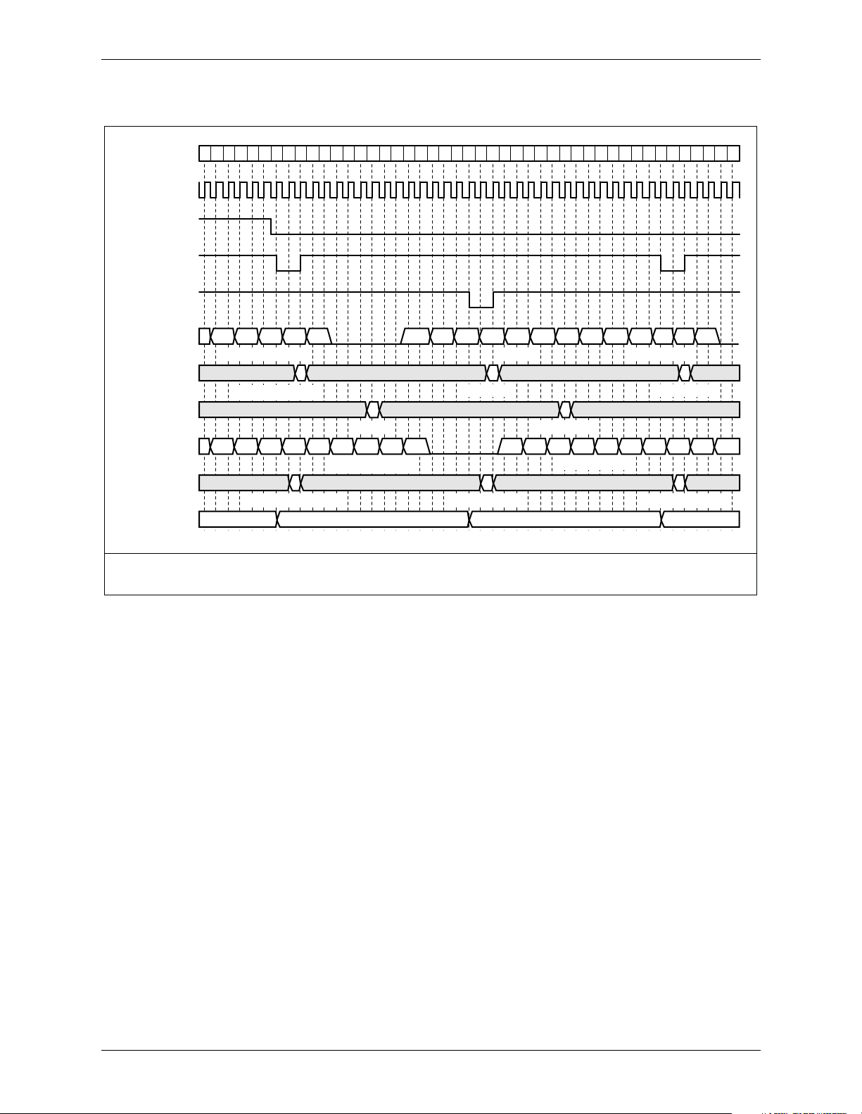
Figure 2-3 illustrates the operation of the Bt8110/8110B in 24- or 32-channel
full-duplex interleaved mode with microprocessor control. The channel numbers
in parentheses are for the 24-channel full-duplex mode. In this diagram, inputs
are shown changing on negative edges of the input clock, and outputs are shown
changing on positive edges. This is the recommended method for operating the
Bt8110/8110B to avoid any timing problems. Detailed timing parameters are
given in Chapter 4.0.
To operate the Bt8110/8110B in the 24- or 32-channel full-duplex interleaved
mode, the Mode Control Register located at address 0x40 should be set to a value
of 0x0C for 32 channels, 0x04 for 24 channels.
In many 24-channel configurations, a gapped clock will be used to account for
the frame bit of the T1 signal; this operates correctly as long as there are exactly
32 clock cycles per channel processed.
2.2 Modes of Operation
100060C Conexant 2-5
Page 26
2.0 Functional Description Bt8110/8110B
2.2 Modes of Operation High-Capacity ADPCM Processor
Figure 2-3. Input and Output Timing for 24- or 32-Channel Full-Duplex Interleaved Operation (Microprocessor Control)
Ref. Cycle
8.192
(6.144) MHz
Clock
SYNC
ADPCM_STB
PCM_STB
4.096
(3.072) Mbit/s
SERIAL_IN
PSIG[7:0]
RESET
SERIAL_OUT
D[7:0]
D[7:0] Int
NOTE(S):
(1) Bt8110B only.
(1)
0 1 2 3 4 5 6 7 8 9 10 11 12 13 14 15 16 17 18 19 20 21 22 23 24 25 26 27 28 29 30 31
I1 I2 I3 I4 I5 I1 I2 I3 I4 I5S 234 5678
ADPCM-31 (23)
ADPCM-31 (23) ADPCM-0PCM-0
ADPCM-0PCM-0
I1 I2 I3 I4 I55678
ADPCM-30 (22)
PCM-29 (21)
ADPCM-30 (22)
PCM-29 (21)
PCM-29 (21)
ADPCM-0PCM-0
I1 I2S23 4 56 78
ADPCM-31 (23)ADPCM-30 (22)
ADPCM-31 (23)
100060_008
2.2.1.1 Signal Inputs
and
Outputs
Either serial or parallel signal inputs can be used in all modes. When the PSIGEN
input is tied high, the parallel signal inputs for both PCM and ADPCM are
enabled.
The SERIAL_IN signal contains the serial PCM encoder input, sign bit first,
and the serial ADPCM input. (The ADPCM values are preceded by I with I1
being the most significant bit.) The input is applied at a rate of 4.096 Mbit/s
(3.072 Mbit/s for 24-channel). The timing is arranged as shown so that the middle
of bit 3 of the ADPCM is coincident with falling edges of SYNC. For codes of
less than 5 bits, the unused serial input ADPCM bits must be set to zero.
The PSIG[7:0] signal is used for the signal input when PSIGEN is high. It is
also used for the ADPCM word length indication when embedded decoding is
performed. Table 2 -2 is the arrangement of the input bits on the bus.
NOTE: On the Bt8110B only, a latch has been added to the parallel input signal
enable, PSIGEN. This signal now has the same input timing as the parallel
input itself. This allows different inputs for the encoder and decoder,
respectively, in interleaved mode, and using the serial input for idle code
insertion under control of PSIGEN when the normal input is parallel
mode, or vice versa.
2-6 Conexant 100060C
Page 27

Bt8110/8110B 2.0 Functional Description
High-Capacity ADPCM Processor
operation where they specify the number of bits in the applied decoder input.
Unused decoder input bits must be set to 0.
Table 2-2. Parallel Signal Input Bus
PSIG[1]. These are used as inputs for embedded decoding. The other PSIG inputs
should be held at a logic low level; these inputs have internal pull-down circuits.
Driving these inputs when only serial inputs are enabled will induce test modes in
the part that will interfere with proper operation.
in Figure 2-3. The ADPCM output is from the channel whose PCM signal was
applied 56 clock cycles previously. The PCM output is from the channel whose
ADPCM input was applied 88 clock cycles previously. Unused ADPCM output
bits are set to 0.
signal outputs at the indicated time. Table 2-3 gives the arrangement of the output
bits on the bus.
2.2 Modes of Operation
Bits e1 and e0 of the decoder input are used only for embedded coding
Input Bus Encoder In Decoder In
PSIG[7] Sign Bit I1
PSIG[6] Bit 2 I2
PSIG[5] Bit 3 I3
PSIG[4] Bit 4 I4
PSIG[3] Bit 5 I5
PSIG[2] Bit 6 e1 - 0 for 3 or 2 bits, 1 for 5 or 4 bits
PSIG[1] Bit 7 e0 - 0 for 4 or 2 bits, 1 for 5 or 3 bits
PSIG[0] Bit 8 0
If PSIGEN is low, the only PSIG[7:0] bus inputs used are PSIG[2] and
SERIAL_OUT represents the timing on the serial ADPCM signals as shown
D[7:0] outputs are the 8 output bits of the ROM and are used for the parallel
NOTE: On Bt8110B only, when internal ROM is used, the bidirect outputs D[7:0]
will contain the PCM/ADPCM output values, MSB on D[7]. Each output
word will be latched simultaneously with the falling edge of the PCM and
ADPCM strobe signals. In interleaved mode, the output timing will appear
as shown by signal D[7:0] Int in Figure 2-3.
The delay of the parallel outputs can be observed in Figure 2-3. When parallel
inputs are used, the ADPCM output for encoder operations is available 48 clock
cycles after the input is applied. The PCM output of decoder operations is
available 80 clock cycles after the input is applied.
When the channel control is set for transparent operation, the 8-bit output
field is exactly the same as the 8-bit input field for either parallel or serial inputs.
The delay is kept the same as for coding operations.
100060C Conexant 2-7
Page 28

2.0 Functional Description Bt8110/8110B
2.2 Modes of Operation High-Capacity ADPCM Processor
Table 2-3. Parallel Signal Output Bus
Output Bus Bit Decoder Out Encoder Out
D[7] Sign Bit I1
D[6] Bit 2 I2
D[5] Bit 3 I3
D[4] Bit 4 I4
D[3] Bit 5 I5
D[2] Bit 6 0
D[1] Bit 7 0
D[0] Bit 8 0
2.2.1.2 Reset Control The RESET signal pin can be used to reset the algorithm according to ANSI
T1.303–1989 and ITU-T G.726 when microprocessor operation mode is used; the
reset control bit [EN_RST; per_chan_ctrl.5] can also set this function. The
real-time algorithm reset function is useful in Digital Circuit Multiplication
Equipment (DCME), packet-voice, and speech storage applications. The RESET
input is active during the time interval shown in Figure 2-3.
2.2.2 48- or 64-Channel Encoder-Only Operation
Figure 2-4 shows the functional timing for 48- or 64-channel half-duplex
encoder-only operation. The channel numbers in parentheses are for the
48-channel encoder-only mode. The timing is generally the same as for
interleaved timing, but the inputs are all PCM for encoding, and the outputs are
all ADPCM. In this mode of operation, the ADPCM_STB signal occurs once
every 16 clock cycles and the PCM_STB signal is not active. This keeps the
ADPCM_STB signal periodic with both the inputs and the outputs when the
parallel input interface is used.
To operate the Bt8110/8110B in the 48- or 64- channel encoder-only mode,
the Mode Control Register should be set to a value of 0x0D for 64 channels or
0x05 for 48 channels. In many 48-channel configurations, a gapped clock will be
used to account for the frame bit of the T1 signal; this operates correctly as long
as there are exactly 32 clock cycles per channel processed.
The address table for the microprocessor per-channel controls
(encoder/decoder operation only) is given in the Register Summary, Ta bl e 3 -4 .
2-8 Conexant 100060C
Page 29

Bt8110/8110B 2.0 Functional Description
High-Capacity ADPCM Processor
Figure 2-4. Input and Output Timing for 48- or 64-Channel Half-Duplex Encoder-Only Operation (Microprocessor Control)
Ref. Cycle
8.192
(6.144) MHz
Clock
SYNC
ADPCM_STB
PCM_STB
4.096
(3.072) Mbit/s
SERIAL_IN
PSIG[7:0]
RESET
SERIAL_OUT
D[7:0]
D[7:0] Int
NOTE(S):
(1) Bt8110B only.
(1)
S 2 3 4 5 6 7 S 2 3 4 5 6 7 8 S 2 3 4 5 68
I5 I1 I2 I1 I2 I1 I2I3 I4I3 I4 I5 I5
0 1 2 3 4 5 6 7 8 9 10 11 12 13 14 15 16 17 18 19 20 21 22 23 24 25 26 27 28 29 30 31
PCM-63 (47)
PCM-63 (47)
PCM-0
ADPCM-60 (44)
ADPCM-60 (44)
PCM-0
PCM-0
PCM-1
ADPCM-61 (45)
ADPCM-61 (45)
2.2 Modes of Operation
PCM-1
PCM-1
ADPCM-62 (46)ADPCM-60 (44)
ADPCM-62 (46)ADPCM-61 (45)
100060_009
2.2.3 48- or 64-Channel Decoder-Only Operation
Figure 2-5 shows the functional timing for 48- or 64-channel decoder-only
operation. The channel numbers in parentheses are for the 48-channel mode.
Again, the timing is generally the same as for interleaved timing, but the inputs
are all ADPCM and the outputs are all PCM. Here, PCM_STB is active every 16
clock cycles, and ADPCM_STB is not active.
To operate the Bt8110/8110B in the 48- or 64-channel decoder-only, the Mode
Control Register should be set to a value of 0x0E for 64 channels or 0x06 for 48
channels.
The address table for the microprocessor per-channel controls
(encoder/decoder-only operation) is the same as for encoder-only operation and is
given in the Register Summary, Ta ble 3 -4 .
100060C Conexant 2-9
Page 30

2.0 Functional Description Bt8110/8110B
2.2 Modes of Operation High-Capacity ADPCM Processor
Figure 2-5. Input and Output Timing for 48- or 64-Channel Half-Duplex Decoder-Only Operation (Microprocessor Control)
Ref. Cycle
8.192
(6.144) MHz
Clock
SYNC
ADPCM_STB
PCM_STB
4.096
(3.072) Mbit/s
SERIAL_IN
PSIG[7:0]
RESET
SERIAL_OUT
D[7:0]
D[7:0] Int
NOTE(S):
(1) Bt8110B only.
(1)
0 1 2 3 4 5 6 7 8 9 10 11 12 13 14 15 16 17 18 19 20 21 22 23 24 25 26 27 28 29 30 31
I1 I2 I3 I4 I2 I3 I4 I2 I3 I4I5 I5 I5I1 I1
ADPCM-63 (47)
ADPCM-63 (47)
ADPCM-0
5 6 7 8 S 2 3 5 6 7 8 S 2 3 4 5 6 7 8 S 24
PCM-58 (42)
PCM-58 (42)
ADPCM-0
ADPCM-1
ADPCM-59 (43)
PCM-59 (43)
ADPCM-1
ADPCM-1ADPCM-0
PCM-60 (44)PCM-58 (42)
PCM-60 (44)PCM-59 (43)
100060_010
2-10 Conexant 100060C
Page 31

Bt8110/8110B 2.0 Functional Description
High-Capacity ADPCM Processor
2.3 Direct Framer Interface Operation
The direct framer interface operation modes are intended for voice compression
and storage applications such as voice mail, voice message store and forward, or
voice response. For more details, see the Speech Compression Interface
application notes, Appendix B and C of this specification.
2.3.1 T1 Framer Interface
In this configuration, address 0x40 must be set to a value of 0x14 to properly set
the Bt8110/8110B mode. The per-channel control registers given in Tabl e 3-3
must be configured for the appropriate code selection, coding type, and
transparency. The Bt8110 allows only 56 kbit/s data rate in transparent mode. The
Bt8110B operates at a full 64 kbit/s data rate. The full-rate PCM signals are serial
and are connected directly to the SERIAL_IN and SERIAL_OUT pins.
parallel interface for the ADPCM inputs PSIG[7:0] and outputs D[7:0]. The
ADPCM inputs and outputs are timed by the signal ADPCM_STB. The ADPCM
input to the Bt8110/8110B is applied to the parallel input PSIG[7:3] with the
most significant bit at PSIG[7]. The ADPCM output is obtained from the Parallel
Signal Output Bus D[7:0] with the most significant bit at D[7].
receive a digital line at the 1.544 Mbit/s rate. The slip buffer of the T1 framer
frame-synchronizes the receive signal to the transmit signal so that the
Bt8110/8110B can operate synchronously on both signals.
the ADPCM output data is valid at the positive edge. Due to the processing delay
of the Bt8110/8110B, there is a five-channel offset between the timing of the
ADPCM input and PCM output.
embedded codes) or less. The ADPCM input includes up to 5 ADPCM input bits
and 2 bits to indicate the number of bits in the decoder input when embedded
encoding is used. On the Bt8110 only, the input to PSIG[0], the least significant
bit, must be left open or held at a logic low level (this pin has an internal
pull-down resistor).
12.352 MHz input clock to the Bt8110. The required 12.352 MHz signal source
should be phase-locked to incoming PCM data. A complete implementation of a
48-channel T1 speech compression interface utilizing the Conexant Bt8300 Dual
T1-Framer and the Bt8110/8110B is detailed in Appendix B, T1 Speech
Compression Interface.
2.3 Direct Framer Interface Operation
In this application, the PSIGEN input must be held low, thus enabling the
The Bt8110/8110B interfaces to a T1 framer, which is used to transmit and
The ADPCM input data must be valid at the positive edge of ADPCM_STB;
The ADPCM output is always 5 bits (for 40 kbit/s coding and for all
The 6.144 MHz clock is obtained by internally dividing and gapping the
100060C Conexant 2-11
Page 32

2.0 Functional Description Bt8110/8110B
2.3 Direct Framer Interface Operation High-Capacity ADPCM Processor
2.3.2 E1 Framer Interface
In this configuration, address 0x40 must be set to a value of 0x1C to properly set
the Bt8110/8110B mode. The per-channel control registers given in Tabl e 3-3
must be configured for the appropriate code selection, coding type, and
transparency. The Bt8110 allows only 56 kbit/s data rate in transparent mode. The
Bt8110B operates at a full 64 kbit/s data rate. The full-rate PCM signals are serial
and are connected directly to the SERIAL_IN and SERIAL_OUT pins.
In this application the PSIGEN input must be held low, thus enabling the
parallel interface for the ADPCM inputs PSIG[7:0] and outputs D[7:0]. The
ADPCM inputs and outputs are timed by the signal ADPCM_STB. The input to
each Bt8110 is applied to the parallel input PSIG[7:0] with the most significant
bit at PSIG[7]. The output is obtained from the ROM data bus D[7:0] with the
most significant bit at D[7].
The Bt8110/8110B interfaces to the E1 framer which transmits and receives a
digital line at the 2.048 Mbit/s primary rate. The slip buffer of the E1 framer
frame-synchronizes the receive signal to the transmit signal allowing the
Bt8110/8110B to operate synchronously on both signals.
The ADPCM input data must be valid at the positive edge of ADPCM_STB;
the ADPCM output data is valid at the positive edge. Due to the processing delay
of the Bt8110/8110B, there is a five-channel offset between the timing of the
ADPCM input and PCM output.
The ADPCM output is always 5 bits (for 40 kbit/s coding and for all
embedded codes) or less. The ADPCM input includes up to 5 ADPCM input bits
and 2 bits to indicate the number of bits in the decoder input when embedded
encoding is used. On the Bt8110 only, the input to PSIG[0], the least significant
bit, must be left open or held at a logic low level (this pin has an internal
pull-down resistor).
The required 8.192 MHz clock source should be phased-locked to incoming
PCM data. A complete implementation of a 60-channel E1 speech compression
interface utilizing the Bt8510 E1 Framer and the Bt8110/8110B is detailed in
Appendix C, E1 Speech Compression Interface.
2-12 Conexant 100060C
Page 33

Bt8110/8110B 2.0 Functional Description
High-Capacity ADPCM Processor
2.4 Hardware Control
Some applications require precise timing of the modification of the code selected,
transparent operation, or coding law. In these cases, the control signals can be
provided by hardware and are updated each time a PCM encoder input or an
ADPCM decoder input is applied. Serial or parallel inputs can be used. Tab le 2 -4 .
defines the functions and inputs of the control pins for hardware control.
Table 2-4. Bt8110/8110B Connection for Hardware Mode
2.4 Hardware Control
Bt8110/8110B
Pin
MICREN µP Enable GND 23
ALE Optional Coding OPT (CODE[3]) 29
WR* Enable A-Law PCM A-LAW 3
CS Enable Transparent TRNSPT 22
Function Hardware Mode Pin #
AD[0] Mode Bit 0 MODE[0] 11
AD[1] Mode Bit 1 MODE[1] 12
AD[2] Mode Bit 2 MODE[2] 13
AD[3] 32-Channel Operation CH32 19
AD[4] Code Bit 0 CODE[0] 24
AD[5] Code Bit 1 CODE[1] 25
AD[6] Embedded Coding EMB (CODE[2]) 28
NOTE(S): The four CODE[n] pins (24, 25, 28, and 29) address the 14 ROM code locations
when using hardware control mode.
100060C Conexant 2-13
Page 34

2.0 Functional Description Bt8110/8110B
2.4 Hardware Control High-Capacity ADPCM Processor
2.4.1 Mode Pins
Mode Control (AD[2:0]) and Enable 32-Channel Operation (AD[3]) control pins
are fixed for a given operational configuration and are not subject to timing
specifications. Mode and control operation pins are defined in Tabl e 2 -5 . The
enable 32-channel operation input is set high for 32- and 64-channel operation
and low for 24- and 48-channel operation.
Table 2-5. Mode Pins
AD[2] AD[1] AD[0] Source
1 0 0 Interleaved
101 Encoder
1 1 0 Decoder
1 1 1 Only used for pre-Bt8110 design compatibility.
001
010
001
011
010
000
NOTE(S):
(1)
See Appendix A for additional information.
Interleaved Processor #1 48/64
Interleaved Processor #2 48/64
Encoder Processor #1 48/64
Encoder Processor #2 48/64
Decoder Processor #1 48/64
Decoder Processor #2 48/64
(1)
(1)
(1)
(1)
(1)
(1)
2.4.2 Control Pins
Four pins control the coding (AD[6:4], ALE), one pin selects the PCM coding law
(WR*), and one pin selects transparent operation (CS). Figure 2-6 illustrates the
functional timing of these inputs. Figure 2-7 and Figure 2-8 detail encoder-only
operation and decoder-only operation, respectively.
The code select input pins have the same timing requirement as the parallel
signal inputs on PSIGEN. The transparent enable and A-law enable controls are
applied two clock cycles after the reset input and six clock cycles before the
coding input. Detailed timing requirements are provided in Chapter 4.0.
2-14 Conexant 100060C
Page 35

Bt8110/8110B 2.0 Functional Description
High-Capacity ADPCM Processor
Figure 2-6. Hardware Control Interleaved Timing
Ref. Cycle
8.192 (6.144)
MHz Clock
SYNC
ADPCM_STB
PCM_STB
4.096
(3.072) Mbit/s
SERIAL_IN
PSIG[7:0]
CODE[1],
CODE[0]
OPT, EMB
RESET
SERIAL_OUT
D[7:0]
D[7:0] Int
I1 I2 I3 I4 2 3 4 5 6 7 8 I1 I2 I3 I4I5
ADPCM-31 (23)
5 6 7 2 3 4 5 6 7 8 I1 I28 I1 I4I2 I3 I5 S
(1)
0 1 2 3 4 5 6 7 8 9 10 11 12 13 14 15 16 17 18 19 20 21 22 23 24 25 26 27 28 29 30 31
ADPCM-31 (23)
PCM-0
ADPCM-30 (22)
ADPCM-30 (22)
PCM-29 (21)
2.4 Hardware Control
I5S
ADPCM-0PCM-0
ADPCM-0PCM-0
ADPCM-0
PCM-29 (21)
ADPCM-31 (23)ADPCM-30 (22)
ADPCM-31 (23)PCM-29 (21)
NOTE(S):
(1) Bt8110B only.
100060_011
100060C Conexant 2-15
Page 36

2.0 Functional Description Bt8110/8110B
2.4 Hardware Control High-Capacity ADPCM Processor
Figure 2-7. Hardware Control Encoder-Only Timing
Ref. Cycle
8.192 (6.144)
MHz Clock
SYNC
ADPCM_STB
PCM_STB
4.096
(3.072) Mbit/s
SERIAL_IN
PSIG[7:0]
CODE[1],
CODE[0]
OPT, EMB
RESET
SERIAL_OUT
D[7:0]
D[7:0] Int
0 1 2 3 4 5 6 7 8 9 10 11 12 13 14 15 16 17 18 19 20 21 22 23 24 25 26 27 28 29 30 31
S 2 3 4 5 6 7 S 2 3 4 5 6 7 8 S 2 3 4 5 68
PCM-63 (47)
PCM-63 (47)
(1)
PCM-0
PCM-0
I2 I3 I4I5 I5I1 I2 I3 I4 I5I1 I2I1
ADPCM-60 (44)
ADPCM-61 (45)
ADPCM-60 (44)
PCM-1
ADPCM-61 (45)
PCM-1
PCM-1PCM-0
ADPCM-62 (46)ADPCM-60 (44)
ADPCM-62 (46)ADPCM-61 (45)
NOTE(S):
(1) Bt8110B only.
100060_012
2-16 Conexant 100060C
Page 37

Bt8110/8110B 2.0 Functional Description
High-Capacity ADPCM Processor
Figure 2-8. Hardware Control Decoder-Only Timing
Ref. Cycle
8.192 (6.144)
MHz Clock
SYNC
ADPCM_STB
PCM_STB
4.096
(3.072) Mbit/s
SERIAL_IN
PSIG[7:0]
CODE[1],
CODE[0]
OPT, EMB
RESET
SERIAL_OUT
D[7:0]
D[7:0] Int
NOTE(S):
(1) Bt8110B only.
5 6 7 8 S 2 3 5 6 7 8 S 2 3 4 5 6 7 8 S 24
(1)
0 1 2 3 4 5 6 7 8 9 10 11 12 13 14 15 16 17 18 19 20 21 22 23 24 25 26 27 28 29 30 31
ADPCM-63 (47)
ADPCM-63 (47)
ADPCM-0
PCM-58 (42)
PCM-58 (42)
I2 I3 I4 I5I2I2 I3 I4 I5 I1
ADPCM-0
PCM-59 (43)
2.4 Hardware Control
I2 I3 I4 I5I1
ADPCM-1
ADPCM-1ADPCM-0
ADPCM-1
ADPCM-59 (43)
PCM-60 (44)PCM-58 (42)
PCM-60 (44)PCM-59 (43)
100060_013
100060C Conexant 2-17
Page 38

2.0 Functional Description Bt8110/8110B
2.4 Hardware Control High-Capacity ADPCM Processor
2-18 Conexant 100060C
Page 39

3
3.0 Registers
NOTE: For a summary of all registers refer to the Register Summary section at the
end of this chapter.
3.1 0x00–0x3F—Per-Channel Control Registers (per_chan_ctrl)
Per-channel Control Registers can be used by the microprocessor to set the code selection, transparency,
algorithm reset, and PCM coding type on a per-channel basis. This capability allows each channel configuration
to be set without having to generate input control signals in hardware for each channel. Per-channel control
registers are write-only. Any attempt by the microprocessor to read these registers will result in erroneous data.
Four code select bits (CODE[3:0]) select up to 14 different codes from ROM. This allows a single
Bt8110/8110B to realize all of the ADPCM coding algorithms contained in the ANSI standards and ITU-T
recommendations for ADPCM coding. Maximum flexibility can be achieved with a single device for all
ADPCM applications. Specific code assignments depend on the coding of the ROM that is a part of the
Bt8110/8110B set. The standard codes that can be provided are the 32 kbit/s code in ITU-T Recommendation
G.726 and ANSI Standard T1.303-1989, the 24 and 40 kbit/s codes given in ANSI Standard T1.303-1989, and
all of the embedded codes in ANSI Standard T1.310-1991 and ITU-T Recommendation G.727. Only six of the
codes can be embedded codes.
6 5 4 3 2 1 0
EN_ALAW EN_RST EN_TRPT CODE[3] CODE[2] CODE[1] CODE[0]
EN_ALAW Enable A-Law Coding—Sets the encoder PCM input and decoder PCM output coding law to
A-law. If this control is not set, the coding law is µ-law.
EN_RST Enable Reset—Causes the algorithm reset input to be continuously applied as long as the bit is
set. This function is according to ANSI Standard T1.303-1989 and is useful for Digital Circuit
Multiplexing Equipment (DCME) functions.
EN_TRPT Enable Transparent Operation—Uses the Bt8110/8110B to transfer the 8-bit input to the
output without any modifications for both encoder and decoder channels. The delay of the
Bt8110/8110B is the same for transparent operation as it is for coded (normal) operation.
CODE[3:0] Code Select—Selects among the 14 codes contained in the ROM lookup table. For the Bt8110
this table is provided by Conexant in a 128 K ROM, upon request. Each code block is 1024
bytes and can be reorganized in the ROM by the user, except for blocks 6 and 7 which are
reserved.
100060C Conexant 3-1
Page 40

3.0 Registers Bt8110/8110B
3.1 0x00–0x3F—Per-Channel Control Registers (per_chan_ctrl) High-Capacity ADPCM Processor
Table 3-1. Bt8110 or Bt8110B with External Lookup Table ROM
CODE[3:0] ROM Code Table
0000 32 kbit/s G.726
0001 24 kbit/s G.726
0010 16 kbit/s G.726/G.727
0011 40 kbit/s G.726
0100 Unused
0101 Unused
0110 Reserved
0111 Reserved
1000 32 kbit/s Conexant (data optimized)
1001 24 kbit/s Tellabs
1010 16 kbit/s Alternate (3-level)
1011 16 kbit/s Alternate (4-level)
1100 G.727 (5,5)—Embedded Code
1101 G.727 (x,4)—Embedded Code
1110 G.727 (x,3)—Embedded Code
1111 G.727 (x,2)—Embedded Code
NOTE(S): See Section 4.1.2, ROM Specification Section.
Table 3-2. Bt8110B Internal Lookup Table ROM (1 of 2)
CODE[3:0] Internal ROM Code Table
0000 32 kbit/s G.726
0001 24 kbit/s G.726
0010 16 kbit/s G.726/G.727
0011 40 kbit/s G.726
0100 32 kbit/s G.721-1984 (16-level)
0101 24 kbit/s Tellabs
0110 16 kbit/s Alternate (4-level)
0111 Not available
1000 32 kbit/s Conexant (data optimized)
1001 Not available
1010 16 kbit/s Alternate (3-level)
1011 16 kbit/s Alternate (4-level)
3-2 Conexant 100060C
Page 41

Bt8110/8110B 3.0 Registers
High-Capacity ADPCM Processor
Table 3-2. Bt8110B Internal Lookup Table ROM (2 of 2)
CODE[3:0] Internal ROM Code Table
1100 G.727 (5,5)—Embedded Code
1101 G.727 (x,4)—Embedded Code
1110 G.727 (x,3)—Embedded Code
1111 G.727 (x,2)—Embedded Code
3.2 0x40—Mode Control Register (mode)
3.2 0x40—Mode Control Register (mode)
A write to address 0x40 will address the mode control registers for all 24 or 32 channels. Five bits are used to
control the mode of operation of the Bt8110/8110B. This register is write-only.
6 5 4 3 2 1 0
RSVD RSVD EN_FRMR EN_32CH MODE[2] MODE[1] MODE[0]
RSVD Reserved—Unused; should be set to a logic low.
EN_FRMR Enable Direct T1/E1 Framer Interface—Set for direct connection to a T1 or E1 framer circuit.
EN_32CH Enable 32-Channel Operation—Set for 32-channel full duplex or 64-channel half-duplex
operation. If it is not set, 24-channel full-duplex or 48-channel half-duplex operation is
obtained.
MODE[2:0] Mode Control—Set to the values required to obtain the desired operating mode configuration
as follows:
Bit 2 Bit 1 Bit 0 Source
100 Interleaved
101 Encoder
1 1 0 Decoder
111 Not Used
100060C Conexant 3-3
Page 42

3.0 Registers Bt8110/8110B
3.2 0x40—Mode Control Register (mode) High-Capacity ADPCM Processor
3-4 Conexant 100060C
Page 43

Bt8110/8110B
High-Capacity ADPCM Processor
Bit Number
7 6 5 4 3 2 1 0
Write
Read/
Label
Register
3
Register Summary
100060C
• • •••••••••
• • •••••••••
• • •••••••••
00 ENC 0 W RSVD EN_ALAW EN_RST EN_TRPT CODE[3] CODE[2] CODE[1] CODE[0]
01 DEC 0 W RSVD EN_ALAW EN_RST EN_TRPT CODE[3] CODE[2] CODE[1] CODE[0]
02 ENC 1 W RSVD EN_ALAW EN_RST EN_TRPT CODE[3] CODE[2] CODE[1] CODE[0]
03 DEC 1 W RSVD EN_ALAW EN_RST EN_TRPT CODE[3] CODE[2] CODE[1] CODE[0]
04 ENC 2 W RSVD EN_ALAW EN_RST EN_TRPT CODE[3] CODE[2] CODE[1] CODE[0]
(hex)
ADDR
Table 3-3. Interleaved Operation
05 DEC 2 W RSVD EN_ALAW EN_RST EN_TRPT CODE[3] CODE[2] CODE[1] CODE[0]
Conexant
• • •••••••••
0x3C ENC 30 W RSVD EN_ALAW EN_RST EN_TRPT CODE[3] CODE[2] CODE[1] CODE[0]
0x3D DEC 30 W RSVD EN_ALAW EN_RST EN_TRPT CODE[3] CODE[2] CODE[1] CODE[0]
0x3F DEC 31 W RSVD EN_ALAW EN_RST EN_TRPT CODE[3] CODE[2] CODE[1] CODE[0]
0x3E ENC 31 W RSVD EN_ALAW EN_RST EN_TRPT CODE[3] CODE[2] CODE[1] CODE[0]
0x40 MODE W RSVD RSVD RSVD EN_FRMR EN_32CH MODE[2] MODE[1] MODE[0]
3-5
Page 44

Bt8110/8110B
Bit Number
High-Capacity ADPCM Processor
Read/
Register
7 6 5 4 3 2 1 0
Write
Label
3-6
• • •••••••••
• • •••••••••
00 ENC/DEC 0 W RSVD EN_ALAW EN_RST EN_TRPT CODE[3] CODE[2] CODE[1] CODE[0]
01 ENC/DEC 1 W RSVD EN_ALAW EN_RST EN_TRPT CODE[3] CODE[2] CODE[1] CODE[0]
(hex)
ADDR
Table 3-4. Encoder/Decoder–Only Operation
02 ENC/DEC 2 W RSVD EN_ALAW EN_RST EN_TRPT CODE[3] CODE[2] CODE[1] CODE[0]
• • •••••••••
0x3F ENC/DEC 63 W RSVD EN_ALAW EN_RST EN_TRPT CODE[3] CODE[2] CODE[1] CODE[0]
0x3E ENC/DEC 62 W RSVD EN_ALAW EN_RST EN_TRPT CODE[3] CODE[2] CODE[1] CODE[0]
0x40 MODE W RSVD RSVD RSVD EN_FRMR EN_32CH MODE[2] MODE[1] MODE[0]
Conexant
100060C
Page 45

4
4.0 Electrical and Mechanical Specifications
4.1 Microprocessor Interface Timing
To enable the microprocessor interface, MICREN must be at a logic high level.
The pinouts for the controller interface are connected as given in Table 2-1 for
either the 8051 or the 68HC11 controller.
Figure 4-1 illustrates the timing requirements for the microprocessor interface
inputs. The WR* control is active low (write) for the 8051 and latches data on the
rising edge and the E control is active high (write) for the 68HC11. The
appropriate input is identified as the write enable signal. The CS input is active
high. Address data is latched on the falling edge of ALE and is independent of the
CS input.
The write cycle time is equal to six system clock cycles, and varies from
360 ns for a 16.384 MHz clock to 960 ns for a 6.144 MHz clock. The write cycle
time is measured from the end of one write cycle (rising edge of WR*) to the
beginning edge of the next write cycle.
Table 4-1. Microprocessor Interface Timing
Parameter Description Min Typ Max
T
ADWRH
T
ADRDL
T
WRW
T
AS
T
AH
T
CLCL
T
DS
(1)
T
DH
T
WR
NOTE(S):
(1)
The external address/data bus capacitance will increase the data hold time if the bus remains undriven.
(2)
Time given is for a nominal 8.192 MHz input clock frequency. The minimum time allowed should be six times the input clock
period. The write cycle time is measured from the end of one write cycle (rising edge of WR*) to the beginning edge of the
next write cycle.
Select to Write High 25 ns ––
Select to Read Low 10 ns ––
Write Pulse Width 25 ns ––
Address Setup before ALE Low 7 ns ––
Address Hold after ALE Low 10 ns ––
ALE Low to Write/Read Low 10 ns ––
Write Data Stable before Write High 25 ns ––
Write Data Hold after Write High 10 ns ––
Write Cycle Time
732 ns
(2)
––
100060C Conexant 4-1
Page 46

4.0 Electrical and Mechanical Specifications Bt8110/8110B
4.1 Microprocessor Interface Timing High-Capacity ADPCM Processor
Figure 4-1. Microprocessor Interface Timing
CS
T
T
CLCL
ADWRH
T
WRW
T
DS
T
DH
100060_014
WR* (8051)
E (68HC11)
AD[6:0]
ALE
T
ADRDL
T
AS
T
AH
4.1.1 Bt8110 Timing
The Bt8110/8110B is a fully static synchronous digital processor. The inputs
MICREN, PSIGEN, and hardware mode AD[3:0] are all configuration inputs and
fixed for a given operating mode.
All other inputs are sampled on positive clock transitions. SERIAL_IN and
D[7:0] inputs are sampled every other clock cycle; other inputs are sampled every
16 clock cycles. The setup and hold times for the ROM data are controlled by the
internal circuits of the Bt8110/8110B to allow operation using a ROM with 0 ns
hold time.
Tables 4 -2 and 4-3 give setup and hold times for all of the inputs and a
reference clock cycle relative to the SYNC signal input for a given channel during
hardware mode operation. All outputs settle within 30 ns (TPDmax) of the
corresponding clock positive transition to less than 0.5 V for logic low outputs
and greater than V
Figure 4-2).
–0.5 V for logic high outputs into a 50 pF load (see
CC
4-2 Conexant 100060C
Page 47

Bt8110/8110B 4.0 Electrical and Mechanical Specifications
High-Capacity ADPCM Processor
Table 4-2. Bt8110/8110B Hardware Mode Timing
4.1 Microprocessor Interface Timing
Signal Name Functions
SYNC Multiframe SYNC 0 0 ns 20 ns
SERIAL_IN Serial PCM/ADPCM Input 0 0 ns 20 ns
RESET Enable Algorithm Reset 9 0 ns 20 ns
CS Enable Transparent Operation 12 0 ns 20 ns
WR* Enable A-Law PCM Coding 12 0 ns 20 ns
PSIG[7:0] Parallel PCM/ADPCM Input 18 0 ns 20 ns
ALE Optional Code Input, CODE[3] 18 0 ns 20 ns
AD[6] Optional Code Input, CODE[2] 18 0 ns 20 ns
AD[5] Optional Code Input, CODE[1] 18 0 ns 20 ns
AD[4] Optional Code Input, CODE[0] 18 0 ns 20 ns
Reference
Cycle
Setup
Time
TSU)
(
Hold
Time
(THD)
Table 4-3. Input and Output Signal Timing
Parameter Description Min Typ Max
T
SU
T
HD
T
PD
Figure 4-2. Input and Output Signal Timing
Clock
Output
Signal
Input Setup Time 0 ns ––
Input Hold Time 20 ns –
Output Setting Time ––30 ns
T
PD
Input Clock
Input Signal
T
SU
T
HD
100060_015
100060C Conexant 4-3
Page 48

4.0 Electrical and Mechanical Specifications Bt8110/8110B
4.1 Microprocessor Interface Timing High-Capacity ADPCM Processor
4.1.2 ROM Specifications
The ROM used as a part of the Bt8110/8110B requires an access time of less than
two clock cycles. The worst-case internal propagation delays total 30 ns requiring
the ROM access time to be 30 ns less than two clock periods. Recommended
access times for the system clock frequencies are shown in Tab l e 4-4.
Table 4-4. System Clock Frequencies
Clock Frequency Access Time
6.144 MHz 250 ns
8.192 MHz 200 ns
12.288 MHz 125 ns
16.384 MHz 90 ns
4-4 Conexant 100060C
Page 49

Bt8110/8110B 4.0 Electrical and Mechanical Specifications
High-Capacity ADPCM Processor
4.2 Absolute Maximum Ratings
The power consumption is proportional to the internal Bt8110/8110B system
clock rate as shown in Table 4 -5 ; however, the ROM power is not included.
Stresses above those listed as Absolute Maximum Ratings may cause
permanent damage to the device. This is a stress rating only, and functional
operation of the device at these or any other conditions above those indicated in
the other sections of this document is not implied. Exposure to absolute
maximum rating conditions for extended periods may affect device reliability.
This device should be handled as an ESD-sensitive device. Voltage on any signal
pin that exceeds the power supply voltage by more than +0.5 V can induce
destructive latchup.
Table 4-5. Absolute Maximum Ratings
Parameter Symbol Value Unit
Supply Voltage V
DD
4.2 Absolute Maximum Ratings
–0.5 to +7.0 Volts
Input Voltage V
Output Voltage V
Operating Temperature TA –40 to +85 °C
Storage Temperature T
Operating Supply Voltage V
Bt8110:
Maximum Current @ 8.192 MHz (internal clk) I
Bt8110B:
Maximum Current @ 8.192 MHz (internal clk) I
IN
OUT
STG
CC
CC
CC
–0.5 to V
–0.5 to V
–55 to +150 °C
+4.75 to +5.25 Volts
+0.5 Volts
DD
+0.5 Volts
DD
96 mA
50 mA
100060C Conexant 4-5
Page 50

4.0 Electrical and Mechanical Specifications Bt8110/8110B
4.3 DC Characteristics High-Capacity ADPCM Processor
4.3 DC Characteristics
All inputs in Table 4-6 have input thresholds compatible with TTL drive levels.
Leakage current for each pin is less than 10 µA in any state. All outputs have
drive current I
CMOS drive levels and can be used with CMOS or TTL logic.
Table 4-6. DC Characteristics
Parameter Description Conditions Min Typ Max Units
= +4 mA at 0.4 V and IOH = –4 mA at 2.4 V. All outputs are
OL
V
DD
V
OH
V
OL
V
IH
V
IL
I
IL
I
OL
C
IN
C
OUT
Bt8110:
I
DD
Bt8110B:
I
DD
Supply Voltage 4.75 5.00 5.25 Volts
All Outputs, AD[6:0] IOH = –4 mA @ VDD = 4.5 V 2.2 4.5 – Volts
All Outputs, AD[6:0] IOL = +4 mA @ VDD = 4.5 V - 0.2 0.45 Volts
Input Voltage High VDD = 4.5 V 3.15 ––Volts
Input Voltage Low VDD = 4.5 V ––1.35 Volts
Input Leakage Current 0V ≥ V
Output Leakage Current 0V ≥ VIN ≥ V
Input Capacitance Inputs and AD[6:0] ––10 pF
Output Capacitance All Outputs ––10 pF
ESD Protection MIL-STD-883C, Method 3015 2 > 3 – kVolts
Latch-up Input JEDEC JC-40.2 150 > 400 – mA
Supply Current V
Supply Current V
IN
≥ V
CC
CC
– ± 1.0 ± 10 µA
– ± 1.0 ± 10 µA
= 5.0 V @ 8.192 MHz ––96 mA
DD
= 5.0 V @ 8.192 MHz 50
DD
4-6 Conexant 100060C
Page 51

Bt8110/8110B 4.0 Electrical and Mechanical Specifications
High-Capacity ADPCM Processor
4.4 Mechanical Specifications
Figure 4-3. 68-Pin Plastic Leaded Chip Carrier (J-Bend)
D
.042"
.048"
X 45˚
PIN 1 IDENTIFIER
D1
68 PLCC
.050" BSC.
4.4 Mechanical Specifications
.042"
.056"
SEE DETAIL 'A'
D2
E2
S
Y
M
B
O
L
A
A
D
D
D
D
E
E
E
E
EE1
1
1
2
3
1
2
3
INCHES MILLIMETERS
MIN.
.165
.090
.985
.950
.445
.985
.950
.445
NOM. NOM.
.800 REF. 20.32 REF.
.800 REF. 20.32 REF.
MAX.
.200
.130
.995
.958
.465
.995
.958
.465
MIN.
4.20
2.29
25.02
24.13
11.30
25.02
24.13
11.30
MAX.
5.08
3.30
25.27
24.33
11.81
25.27
24.33
11.81
D3
E3
D2
E2
A1
A
.025"/.045" R
.026"
.032"
.013"
.021"
.020" MIN.
DETAIL "A"
100060_016
100060C Conexant 4-7
Page 52

4.0 Electrical and Mechanical Specifications Bt8110/8110B
4.4 Mechanical Specifications High-Capacity ADPCM Processor
4-8 Conexant 100060C
Page 53

A.1.1 Introduction
A
Appendix A. Hardware Mode Operation
A.1 48- or 64-Channel Full-Duplex Hardware Mode Operation
This appendix details the Bt8110/8110B ADPCM Processor 48- or 64-channel
operation. This configuration may be used in conjunction with the Bt8200
ADPCM Line Formatter to build a 2:1 ADPCM transcoder. The interface
nomenclature in Figure A-1 corresponds to that used with the T1 and E1
transcoder evaluation boards (Bt8200EVM–T1 and Bt8200EVM–E1). See
Appendix D and E.
Two Bt8110/8110B 24- or 32-channel processors (combined with a single
external ROM for the Bt8110) will process either 48 or 64 full-duplex channels
using interleaved encoder/decoder processing. This combination may also be
programmed to alternately process 96 or 128 encode-only or decode-only
channels.
A.1.2 Configuration
A block diagram showing the configuration of the Bt8110/8110B for 48- or
64-channel operation is shown in Figure A-1. The two Bt8110/8110Bs share all
of the input and output signals and the external ROM to appear to external
interfaces as a single functional device, and each takes turns reading the ROM to
obtain the required outputs.
100060C Conexant A-1
Page 54

Appendix A . Hardware Mode Operation Bt8110/8110B
A.1 48- or 64-Channel Full-Duplex Hardware Mode Operation High-Capacity ADPCM Processor
Figure A-1. 48- or 64-Channel Configuration of the Bt8110/8110B
CLOCK
SYNC
LAW
64 CHANNEL
SERIAL_IN
CNTRL
CODE12
CODE13
CLOCK
SYNC
LAW
64 CHANNEL
SERIAL_IN
CNTRL
CODE12
CODE13
CLOCK
SYNC
WR*
AD[3]
SERIAL_IN
RESET, CS
AD[4]
AD[5]
D[7:0]
CLOCK
SYNC
WR*
AD[3]
SERIAL_IN
RESET, CS
AD[4]
AD[5]
D[7:0]
ADPCM
Processor
Bt8110/8110B
ADPCM
Processor
Bt8110/8110B
SERIAL_OUT
A[13:0]
A[13:0]
SERIAL_OUT
SERIAL_OUT
External
ROM
100060_017
The two Bt8110/8110Bs need to have the three mode control pins set to enable
interleaved, encoder, or decoder modes; and processor number. In interleaved
mode, the circuit will realize 48 or 64 full-duplex channels of ADPCM coding. In
encoder mode, 96 or 128 encoders are realized. In decoder mode, 96 or 128
decoders are realized. To set the modes, the inputs AD[2], AD[1], and AD[0]
need to be set as shown in Tabl e A-1.
Table A-1. Mode Settings
Pin Name
Interleaved Mode 0 0 1 0 1 0
Encoder Mode 0 0 1 0 1 1
Decoder Mode 0 1 0 0 0 0
Processor Number 1
AD[2] AD[1] AD[0]
Processor Number 1 and Processor Number 2 must be designated as such
because, in this configuration, each Bt8110/8110B responds to alternate groups
of 16 clock cycles (12.288 or 16.384 MHz). The Number 1 and Number 2
designation is arbitrary and is not influenced by any other part of the circuitry.
Processor Number 2
AD[2] AD[1] AD[0]
A-2 Conexant 100060C
Page 55

Bt8110/8110B Appendix A . Hardware Mode Operation
High-Capacity ADPCM Processor
used. However, the Bt8110/8110B has a parallel signal input capability. If
PSIGEN is connected to the supply voltage, the parallel signal input is enabled.
(pins 20 and 22). The RESET input controls the algorithm reset function
according to ANSI Standard T1.303–1989/ITU-T G.7.26 and the CS input
controls transparency (the passthrough of the 8-bit input without encoding or
decoding).
A.1.3 Functional Timing
Functional timing diagrams are given in Figure A-2 through Figure A-4 for
interleaved operation, encoder-only operation, and decoder-only operation,
respectively. The CLOCK signal has a frequency of 16.384 MHz for 64-channel
full-duplex or 128-channel half-duplex operation, and 12.288 MHz for
48-channel or 96-channel half-duplex operation. The SYNC signal is used to
identify channel 1 and is required at any multiple of 32 clock periods. Details of
the timing are given in Chapter 4.0.
for 48-channel full-duplex operation or for 96-channel half-duplex (encoder- or
decoder-only) operation.
A.1 48- or 64-Channel Full-Duplex Hardware Mode Operation
In addition, MICREN and PSIGEN must be held low if the serial inputs are
Note that the CNTRL input is connected to both the RESET and the CS inputs
For each mode, the channels are numbered. The numbers in parentheses are
Figure A-2. 48- or 64-Channel Full-Duplex Interleaved Mode Functional Timing
Ref. Cycle
16.384 (12.288)
MHz CLOCK
SYNC
ADPCM_STB
PCM_STB
8.192 (6.144)
Mbit/s
SERIAL_IN
PSIG[7:0]
RESET,CS
SERIAL_OUT
D[7:0]
D[7:0] Int
ADPCM-63 (47)
(1)
0 1 2 3 4 5 6 7 8 9 10 11 12 13 14 15 16 17 18 19 20 21 22 23 24 25 26 27 28 29 30 31
I2I1 I3 I4 I5
ADPCM-63 (47)
PCM-0
65 7 8 I1 I4 2 3 4 5 6 7 8 I1 I2I2 I3 I5
ADPCM-62 (46)
ADPCM-62 (46)
2 3 4 7 8 I1 I2 I3 I45 6 I5S
S
PCM-61 (45)
ADPCM-0PCM-0
ADPCM-0PCM-0
ADPCM-0
PCM-61 (45)
ADPCM-63 (47)ADPCM-62 (46)
ADPCM-63 (47)PCM-61 (45)
NOTE(S):
(1) Bt8110B only.
100060C Conexant A-3
100060_018
Page 56

Appendix A . Hardware Mode Operation Bt8110/8110B
A.1 48- or 64-Channel Full-Duplex Hardware Mode Operation High-Capacity ADPCM Processor
Figure A-3. 96- or 128-Channel Half-Duplex Encoder-Only Functional Timing
Ref. Cycle
16.384 (12.288)
MHz CLOCK
SYNC
ADPCM_STB
PCM_STB
8.192 (6.144)
Mbit/s
SERIAL_IN
PSIG[7:0]
RESET,CS
SERIAL_OUT
D[7:0]
D[7:0] Int
NOTE(S):
(1) Bt8110B only.
0 1 2 3 4 5 6 7 8 9 10 11 12 13 14 15 16 17 18 19 20 21 22 23 24 25 26 27 28 29 30 31
S 2 3 4 5 6 7 S 2 3 4 5 6 7 8 S 2 3 4 5 68
PCM-127 (95)
PCM-127 (95)
I5
(1)
PCM-0
PCM-0
I2 I3 I4 I5I1 I2 I3 I4 I5I1 I2I1
ADPCM-124 (92)
ADPCM-125 (93)
ADPCM-124 (92)
PCM-1
ADPCM-125 (93)
PCM-1
PCM-1PCM-0
ADPCM-126 (94)ADPCM-124 (92)
ADPCM--126 (94)ADPCM-125 (93)
100060_019
A-4 Conexant 100060C
Page 57

Bt8110/8110B Appendix A . Hardware Mode Operation
High-Capacity ADPCM Processor
Figure A-4. 96- or 128-Channel Half-Duplex Decoder-Only Functional Timing
Ref. Cycle
16.384 (12.288)
MHz CLOCK
SYNC
ADPCM_STB
PCM_STB
8.192 (6.144)
Mbit/s
SERIAL_IN
PSIG[7:0]
RESET,CS
SERIAL_OUT
D[7:0]
D[7:0] Int
NOTE(S):
(1) Bt8110B only.
567 S2 34 5678S2345 6788 S2
(1)
0 1 2 3 4 5 6 7 8 9 10 11 12 13 14 15 16 17 18 19 20 21 22 23 24 25 26 27 28 29 30 31
I2I1 I3 I4 I5
ADPCM-127 (95)
ADPCM-127 (95)
ADPCM-0
PCM-122 (90)
PCM-122 (90)
A.1 48- or 64-Channel Full-Duplex Hardware Mode Operation
I2 I3 I4 I5I1 I2 I3 I4 I5I1
ADPCM-0
PCM-123 (91)
ADPCM-1
ADPCM-1ADPCM-0
ADPCM-1
ADPCM-123 (91)
PCM-124 (92)PCM-122 (90)
PCM-124 (92)PCM-123 (91)
100060_020
100060C Conexant A-5
Page 58

Appendix A . Hardware Mode Operation Bt8110/8110B
A.1 48- or 64-Channel Full-Duplex Hardware Mode Operation High-Capacity ADPCM Processor
A-6 Conexant 100060C
Page 59

B
Appendix B. T1 Speech Compression
B.1 Introduction
This appendix details the operation of the Bt8110/8110B ADPCM Processor with
the Bt8300 Dual T1 Framer for application to speech compression. This operation
mode can be used to provide full-duplex speech compression to 16, 24, 32, or
40 kbit/s using a variety of embedded and non-embedded codes.
The Bt8110/8110B provides the coding algorithms specified in ITU–T
Recommendation G.726 and ANSI Standard T1.303-1989 at 40, 32, 24, or
16 kbit/s. It also provides the embedded codes in ANSI Standard T1.310-1991
and ITU-T Recommendation G.727. The 32 kbit/s ADPCM algorithm is also
specified in the AMIS version 1 digital messaging protocol.
The speech compression application for 48 channels uses the Bt8300 with an
associated 2 K x 8 RAM; two Bt8110/8110Bs, (each with an associated 128 K
ROM for the Bt8110); and a microprocessor for configuration and control. Up to
14 separate coding algorithms can be selected by the microprocessor. An
evaluation board is available for this configuration (part number Bt8113EVM).
Although this application note and the Bt8113EVM both use the Bt8300 Dual T1
Framer (with external RAM), one or two Bt8360 Single T1 Framers (with internal
RAM) can be used with one or two Bt8110/8110Bs for 24 or 48 voice channels,
respectively. The Bt8360 is a newer generation product and offers more voiceand signaling-related features than the Bt8300. For an even higher level of
integration and functionality, a Bt8370 framer with integral LIU can be used.
B.1.1 Configuration
The configuration of the Bt8110/8110B and the Bt8300 is shown in Figure B-1.
The Bt8300 is used to transmit and receive two T1 lines. The slip buffers of the
Bt8300 are used to synchronize the transmit and receive signals of both T1s for
the Bt8110/8110B.
100060C Conexant B-1
Page 60

Appendix B . T1 Speech Compression Bt8110/8110B
B.1 Introduction High-Capacity ADPCM Processor
Figure B-1. T1 Speech Compression Interface Block Diagram
ADPCM
Processor
Bt8110/8110B
CLOCK
SYNC
SERIAL_IN
SERIAL_OUT
ADPCM
Processor
Bt8110/8110B
CLOCK
SYNC
SERIAL_IN
SERIAL_OUT
EXT
ROM
PSIG[7:0]
PSIGEN
PSIG[0]
D[7:0]
8
PSIG[7:0]
PSIGEN
PSIG[0]
D[7:0]
8
PSIG (ADPCM Input)
GND
ADPCM_STB
PCM_STB
D (ADPCM Output)
8
PSIG (ADPCM Input)
GND
ADPCM_STB
PCM_STB
TX A CLK
TX B CLK
Dual T1
Framer
Bt8300
12.352 MHz
Oscillator
1.544 CLK
TX SYNC A OUT
REC SLIP BUFF A
REC SLIP BUFF B
12 MHz CLK
TX SYNC B IN
TX PCM A
TX PCM B
Microprocessor
EXT
ROM
8
D (ADPCM Output)
100060_021
A single microprocessor can be used to control the Bt8300 and the two
Bt8110/8110Bs. The only requirement for the Bt8110/8110B control is to
configure the operating mode and the per-channel control registers that set the
code rate and the A-law/µ-law, and reset the algorithm on each channel, as
desired.
The 12.352 MHz signal source required for the Bt8300 is also used for the
Bt8110 clock. To maintain proper synchronization of the Bt8110/8110B, an exact
12.352 MHz source that is eight times the slip-buffer clock rate (which is the
same as the transmit A PCM clock) must be used. This source can be
phase-locked to one of the received clocks from the T1 line or to a local clock
source. The slip-buffer clock and the transmit clock for the B side of the framer
can then be obtained from the 1.544 MHz clock output from the Bt8300. If the
12.352 MHz clock source is not locked to the line, then the encoder buffer will
have frame slips where one sample of PCM is either repeated or deleted before
encoding to ADPCM. For speech signals, this impairment may be insignificant.
The full-rate PCM inputs and outputs to the Bt8110/8110B are serial and are
configured to connect directly to the Bt8300. The SERIAL_IN and
SERIAL_OUT signals of the Bt8110/8110B connect directly to the slip buffer
output and the transmit input of the framer, respectively. The frame
synchronization is determined by the SYNC input, which can be obtained from
B-2 Conexant 100060C
Page 61

Bt8110/8110B Appendix B . T1 Speech Compression
High-Capacity ADPCM Processor
the free-running synchronization signal TX SYNC A on the Bt8300 (this signal
must also be connected to TX SYNC B IN to synchronize the B side transmitter).
The Bt8110/8110B clock of 6.144 MHz is obtained by internally dividing and
gapping the 12.352 MHz input clock to the Bt8110/8110B.
signal will be identical at both Bt8110/8110Bs. The input to each is applied to the
parallel input PSIG[7:0], with the most significant bit at PSIG[7]. The output is
obtained from the parallel signal output D[7:0], with the most significant bit at
D[7].
output data is valid at the positive edge. Due to the processing delay of the
Bt8110/8110B, there is a five-channel offset between the timing of the ADPCM
input and PCM output.
embedded codes). The ADPCM input includes up to 5 ADPCM input bits and 2
bits to indicate the number of bits in the decoder input when embedded encoding
is used.
microprocessor interface. The PSIGEN pin must be held low. If the RESET input
is not used to reset the algorithm externally, it should be held low; otherwise it
should be generated. The RESET input is active high.
B.1 Introduction
The ADPCM inputs and outputs are timed by the signal ADPCM_STB. This
The input data must be valid at the positive edge of ADPCM_STB and the
The ADPCM output is always 5 bits or less (for 40 kbit/s coding and for all
The MICREN input must be connected to the supply voltage to enable the
B.1.2 Functional Timing Diagram
The timing of the T1 speech compression interface circuit is given in Figure B-2.
The clock signal is 12.352 MHz and is applied to the Bt8300 and both
Bt8110/8110Bs.
The SYNC signal to the Bt8110/8110B is the multiframe synchronization
output of the Bt8300. This signal provides bit and channel synchronization to the
Bt8110/8110Bs. The SYNC signal has a period of 3 ms; the timing diagram
shows the beginning of the frame at the end of the 3 ms period.
The ADPCM_STB signal is an enable and clock output for the
Bt8110/8110Bs. Its positive edge occurs when the ADPCM input is clocked into
the circuit and the ADPCM output is available from the ROM data pins. The
frame-bit location can be identified from the wide interval on this signal, which
occurs once per frame.
The PCM serial input and output timing is determined by the Bt8300
synchronization. The two parts are designed so that as long as the clocks and
synchronization signals are provided as shown in Figure B-1, the serial interface
will operate properly. Each of the signals is clocked by the respective input
circuitry near the middle of the signaling interval, so the interconnection circuitry
is not critical. This makes it possible, for instance, to add drop-and-insert or other
processing functions at the PCM interface.
NOTE: The ADPCM inputs are taken from the parallel input PSIG[7:0] for the
Bt8110B, and PSIG[7:1] for the Bt8110. The outputs are available on the
ROM data output D[7:0] for the Bt8110B, and D[7:1] for the Bt8110. Note
that encoding is provided for the timeslots that normally carry framing and
signaling information.
100060C Conexant B-3
Page 62

Appendix B . T1 Speech Compression Bt8110/8110B
B.1 Introduction High-Capacity ADPCM Processor
There is an offset in the timing between the input and the output signals
caused by the processing delay of the Bt8110/8110B. In Figure B-2, ADPCM-3 is
the encoded output from PCM-3 and ADPCM-22 results in the decoded PCM-22.
This offset must be accounted for in the processing for speech signals or can be
eliminated by delaying the encoded output by 19 channel counts.
If the RESET input pin is used to reset the ADPCM algorithm according to
ANSI Standard T1.303–1989 and ITU-T G.726, the timing is as shown in the
Figure B-2. Note that the RESET input has to be applied approximately 2 µs
before the corresponding ADPCM input; it is possible to use the PCM_STB
signal to latch reset inputs for the ADPCM signal stream and the ADPCM_STB
signal to latch reset inputs for the PCM input stream.
In 48-channel designs, it may be helpful to have a single interleaved parallel
bus. The signal PCM_STB, which is also an output from each Bt8110/8110B, can
be used to clock odd inputs and outputs on and off a single parallel bus.
Figure B-2. T1 Speech Compression Functional Timing Diagram
12.352
MHz CLOCK
6.176 MHz
INT. CLK
SYNC
ADPCM_STB
1.544 Mbit/s
SERIAL_IN
1.544 Mbit/s
SERIAL_OUT
PSIG[7:0]
D[7:0]
ADPCM-22
PCM_STB
RESET
D[7:0] Int
NOTE(S):
(1) Bt8110B only.
(1)
8S234 5678
PCM-24
8S234 5678 S 23 4567 8 S234
PCM-24
ADPCM-3
PCM-1
PCM-1
FS2345678S234
ADPCM-23ADPCM-22 ADPCM-24PCM-1
ADPCM-5ADPCM-4
ADPCM-24PCM-2ADPCM-23
PCM-2
PCM-2PCM-1
PCM-2PCM-1
PCM-3ADPCM-5PCM-2ADPCM-4
100060_022
B-4 Conexant 100060C
Page 63

Bt8110/8110B Appendix B . T1 Speech Compression
High-Capacity ADPCM Processor
B.1.3 Microprocessor Interface And Per-Channel Configuration
The microprocessor interface of the Bt8300 provides all control and status
functions for the T1 lines; it can also be used to insert and extract signaling in this
application.
Table B -1 lists the connections for the Bt8110/8110B. Only 7 bits of the
address/data bus are required. The Bt8110/8110B can be operated by either an
8051-type or a 68HC11-type interface. Only the 8051-type connections are given
here, since the Bt8300 requires this interface. The 68HC11 microprocessor can be
used as well; two gates are required to derive the read and write control signals
needed to emulate the 8051. The Bt8360 T1 Framer and the Bt8370 T1/E1
Framer/LIU interface directly with either the 8051-type or the 68HC11-type
microprocessor.
Table B-1. Bt8110/8110B Microprocessor Connection
ADPCM Processor Pin Function Intel 8051
MICREN Enable V
ALE Address Latch Enable ALE
WR* Write Enable WR*
B.1 Introduction
cc
CS Chip Select A-n
AD[0] Address/Data AD[0]
AD[1] Address/Data AD[1]
AD[2] Address/Data AD[2]
AD[3] Address/Data AD[3]
AD[4] Address/Data AD[4]
AD[5] Address/Data AD[5]
AD[6] Address/Data AD[6]
Table B -2 lists the address map and the bit interpretations of the control fields.
In this application address 0x40 must be set to a value of 0x14 to properly set the
mode of the Bt8110/8110B. A write to any address in the range 0x40–0x3F will
cause the mode of the Bt8110/8110B to be set.
Table B -2 also provides the per-channel control register bit interpretations.
Bits D[3:0] of each encoder and decoder channel control select the particular
ADPCM code to be used; note that hex values of 6 and 7 are invalid for these bit
positions. ROM codes are available from Conexant with the evaluation board. Bit
D[6] enables A-law PCM coding when set. Bit D[5] enables the algorithm
RESET function. This operation sets the internal parameters of the Bt8110/8110B
to fixed values, as specified in ANSI Standard T1.303-1989 and ITU-T G.726.
Bit D[4] enables transparent operation.
For the encoder channels, when the transparent bit is set all 8 PCM bits are
transferred to the output with the same delay as when ADPCM encoding is taking
place. Full 8-bit (64 kbit/s) transparent operation is not a valid option for the T1
speech compression interface configuration using the Bt8110/8110B. 64 kbit/s
transparent operation is valid with the Bt8110/8110BB. For the decoder, the five
ADPCM inputs and two embedded encoding inputs are transferred to the PCM
100060C Conexant B-5
Page 64

Appendix B . T1 Speech Compression Bt8110/8110B
B.1 Introduction High-Capacity ADPCM Processor
serial output with the same delay as when ADPCM decoding is taking place. The
input to PSIG[0], the LSB, must be held at a logic low level in this application.
Table B-2. Microcontroller Memory Map
Address
(hex)
0 Encoder 0 Control
1 Decoder 0 Control
2 Encoder 1 Control
••
••
••
Interleaved Operation
0x3E Encoder 31 Control
0x3F Decoder 31 Control
0x40 Mode Control
0 Encoder/Decoder 0 Control
1 Encoder/Decoder 1 Control
2 Encoder/Decoder 2 Control
••
••
••
Function
0x3E Encoder/Decoder 62 Control
Encoder/Decoder-Only Operation
Register
Mode Control
Control Register
Encoder/Decoder
0x3F Encoder/Decoder 63 Control
0x40 Mode Control
Bit Function
D[2:0] Operation Mode
D[3] 32/64-Channel Operation
D[4] Serial PCM, Parallel ADPCM Mode
D[3:0] Code Select (codes 6, 7 are invalid)
D[4} Set Encoder/Decoder Transparent
D[5] Reset Encoder/Decoder
D[6] Set Encoder/Decoder to A-Law PCM
B-6 Conexant 100060C
Page 65

Bt8110/8110B Appendix B . T1 Speech Compression
High-Capacity ADPCM Processor
This table is a cross-reference between the encoder and decoder addresses and the
PCM channel timeslots.
Table B-3. Bt8110/8110B Processor Per-Channel Control Locations
B.1 Introduction
Table B -3 shows the encoder and decoder locations for each PCM channel.
PCM Channel Encoder Decoder
Channel 1 00 29
Channel 2 02 2B
Channel 3 04 2D
Channel 4 06 2F
Channel 5 08 01
Channel 6 0A 03
Channel 7 0C 05
Channel 8 0E 07
Channel 9 10 09
Channel 10 12 0B
Channel 11 14 0D
Channel 12 16 0F
Channel 13 18 11
Channel 14 1A 13
Channel 15 1C 15
Channel 16 1E 17
Channel 17 20 19
Channel 18 22 1B
Channel 19 24 1D
Channel 20 26 1F
Channel 21 28 21
Channel 22 2A 23
Channel 23 2C 25
Channel 24 2E 27
100060C Conexant B-7
Page 66

Appendix B . T1 Speech Compression Bt8110/8110B
B.1 Introduction High-Capacity ADPCM Processor
B-8 Conexant 100060C
Page 67

C
Appendix C. E1 Speech Compression
C.1 Introduction
This appendix details of operation of the Bt8110/8110B ADPCM Processor with
the Bt8510 E1 Framer/LIU (or Bt8370 T1/E1 Framer/LIU) for application to
speech compression. This mode can be used to provide full-duplex speech
compression to 16, 24, 32, or 40 kbit/s using a number of embedded and
non-embedded codes.
The Bt8110/8110B provides the coding algorithms specified in ITU–T
Recommendation G.726 and ANSI Standard T1.303-1989 at 40, 32, 24, and 16
kbit/s. It also provides the embedded codes in ITU–T Recommendation G.727
and ANSI Standard T1.310-1991. The 32 kbit/s ADPCM algorithm is also used
in the AMIS version 1 digital messaging protocol.
The speech compression application for 30 channels requires a Bt8510 E1
Framer circuit, a Bt8110/8110B (with an associated 128 K ROM for the Bt8110),
and a microprocessor for configuration and control. Up to 14 separate coding
algorithms can be selected by the controller on a channel-by-channel basis. This
application requires approximately 20 square inches and approximately 1.5 Watts
of power from a +5 V supply.
C.1.1 Configuration
Figure C-1 illustrates a configuration of the Bt8110/8110B and the Bt8510. The
Bt8510 transmits and receives a digital line at the 2.048 Mbit/s primary rate. The
slip buffer of the Bt8510 frame-synchronizes the receive signal to the transmit
signal so that the Bt8110/8110B can operate synchronously on both signals.
A single microprocessor can be used to control the Bt8510 and the
Bt8110/8110B. The only control requirement of the microprocessor is to
configure the operating mode and the per-channel control registers that set the
code rate and reset the algorithm on each channel, as desired. The Bt8510 and the
Bt8110/8110B each have a chip select input that can be used to select the desired
device.
The Bt8510 includes an integral digital timing recovery circuit and analog
interface that is compatible with either 75
meets the requirements of ITU–T Recommendation G.703. The timing recovery
circuit requires a 32.768 MHz clock signal. The Bt8510 provides a 16.384 MHz
output which can be divided by 2 to provide the 8.192 MHz clock required by the
Bt8110/8110B and can also be provided to the system clock input.
100060C Conexant C-1
Ω cable or 120 Ω twisted-pair wire and
Page 68

Appendix C . E1 Speech Compression Bt8110/8110B
C.1 Introduction High-Capacity ADPCM Processor
A 2.048 MHz bit clock is then provided at BITCKO. This bit clock is used as
the clock input to both the transmitter circuit and the slip buffer circuit. This
procedure ensures proper alignment of the Bt8110/8110B bit and system clocks.
Figure C-1. E1 Speech Compression Interface Configuration
32.768 MHz
VCXO
CK160
SYSCKI
SLPSYNCI
XYSNCO
SLPPCMO
E1
Framer
Bt8510
Microprocessor
XPCMI
BITCKO
SLPCKI
XSYNCI
8
ADPCM_Input
ADPCM_STB
PCM_STB
+5 V
D (ADPCM Output)
XCKI
÷2
CLOCK
SYNC
SERIAL_IN
SERIAL_OUT
ADPCM
Processor
Bt8110/B
EXT
ROM
PSIG[7:0]
MICREN
RESET
PSIGEN
PSIG[0]
D[7:0]A[13:0]
8
If the 32.768 MHz signal source is then phase-locked to the received clock (by
phase-locking the slip buffer sync output to the receive sync output) then the
transmit and receive clocks will be synchronized and no frame slips will appear at
the receiver.
The full-rate PCM inputs and outputs to the Bt8110/8110B are serial and are
configured to connect directly to the Bt8510. The SERIAL_IN and
SERIAL_OUT signals of the Bt8110/8110B connect directly to the slip buffer
output and the transmit input of the framer, respectively. The Bt8110/8110B
frame synchronization is determined by the SYNC input, which can be obtained
from the free-running synchronization signal XSYNCO from the Bt8510 (this
signal must also be connected to SLPSYNCI to synchronize the receive slip
buffer).
The ADPCM inputs and outputs are timed by the signal ADPCM_STB. The
input to the Bt8110/8110B is applied to the parallel input PSIG[7:0], with the
most significant bit at PSIG[7]. The output is obtained from the ROM data bus
D[7:0], with the most significant bit at D[7].
The input data must be valid at the positive edge of ADPCM_STB and the
output data is valid at the positive edge. Due to the processing delay of the
Bt8110/8110B, there is a five-channel offset between the timing of the ADPCM
input and output.
The ADPCM output is always 5 bits (for 40 kbit/s coding and for all
embedded codes) or less. The input includes up to 5 ADPCM input bits and 2 bits
to indicate the number of bits in the decoder input when embedded encoding is
used.
100060_023
C-2 Conexant 100060C
Page 69

Bt8110/8110B Appendix C . E1 Speech Compression
High-Capacity ADPCM Processor
The MICREN input must be connected to the supply voltage to enable the
microprocessor interface. The PSIGEN pin must be held at a logic low level. If
the RESET input is not used to reset the algorithm externally, it should be
connected to ground as shown in Figure C-1; otherwise it should be generated.
The RESET input is active high.
C.1.2 Functional Timing Diagram
Figure C-2 illustrates the timing of the Bt8110/8110B circuit. The CLOCK signal
is 8.192 MHz and is applied to the Bt8110/8110B. The SYNC signal to the
Bt8110/8110B is the multiframe synchronization output of the Bt8510. This
signal provides channel synchronization to the Bt8110/8110B. The SYNC signal
has a period of 2 ms; the timing diagram shows the beginning of the frame at the
end of the 2 ms period.
The ADPCM_STB signal is an enable and clock output for the Bt8110/8110B.
Its positive edge occurs when the ADPCM input is clocked into the circuit and the
ADPCM output is available from the ROM data pins.
The PCM serial input and output timing is determined by the Bt8510
synchronization. The two parts are designed so that as long as the clocks and
synchronization signals are provided as shown in Figure C-1, the serial interface
will operate properly. Each of the signals is clocked by the respective input
circuitry near the middle of the signaling interval, so the interconnection circuitry
is not critical. This makes it possible to add drop-and-insert or other processing
functions at the serial PCM interface.
C.1 Introduction
NOTE: The ADPCM inputs are taken from the parallel input PSIG[7:0] for the
Bt8110B, and PSIG[7:1] for the Bt8110. The outputs are available on the
ROM data output D[7:0] for the Bt8110B, and D[7:1] for the Bt8110. Note
that encoding is provided for the timeslots that normally carry framing and
signaling information.
There is an offset in the timing between the input and the output signals
caused by the processing delay of the Bt8110/8110B. In Figure C-2, ADPCM-3 is
the encoded output from PCM-3 and ADPCM-30 results in the decoded PCM-30.
This offset must be accounted for in the processing for speech signals, or can be
eliminated by delaying the encoded output by 27 channel counts.
If the RESET input pin is used to reset the ADPCM algorithm according to
ANSI Standard T1.303–1989 and ITU-T G.726, the timing is as shown in the
Figure C-2. Note that the RESET input has to be applied approximately 2 µs
before the corresponding ADPCM input; it is possible to use the PCM_STB
signal to latch reset inputs for the ADPCM signal stream and the ADPCM_STB
signal to latch reset inputs for the PCM input stream.
100060C Conexant C-3
Page 70

Appendix C . E1 Speech Compression Bt8110/8110B
C.1 Introduction High-Capacity ADPCM Processor
Figure C-2. E1 Speech Compression Functional Timing Diagram
8.192 MHz
CLOCK
SYNC
ADPCM_STB
2.048 Mbit/s
SERIAL_IN
2.048 Mbit/s
SERIAL_OUT
PSIG[7:0],
CODE[1,0],
OPT, EMB
D[7:0]
PCM_STB
RESET
D[7:0] Int
NOTE(S):
(1) Bt8110B only.
(1)
8S23456 7 8
PCM-31 (Frame 15)
8S23456 7 8
PCM-31
ADPCM-2
ADPCM-29
PCM-0
PCM-0
PCM-0
S23456 7 8
S23456 7 8
ADPCM-4ADPCM-3
PCM-1
PCM-1ADPCM-29
S2345
PCM-1PCM-0 (Frame 0)
S2345
PCM-1PCM-0
ADPCM-31ADPCM-30
PCM-2ADPCM-4PCM-1ADPCM-3
ADPCM-31ADPCM-30
100060_024
C-4 Conexant 100060C
Page 71

Bt8110/8110B Appendix C . E1 Speech Compression
High-Capacity ADPCM Processor
C.1.3 Microprocessor Interface and Per-Channel Configuration
The microprocessor interface of the Bt8510 provides all control and status
functions for the E1 lines; it can also be used to insert and extract signaling in this
application.
The connections for the Bt8110/8110B are given in Tab le C -1. Only 7 bits of
the address/data bus are required. Any one of the six upper address bits, A[13:8],
of the microprocessor can be used as a chip select signal. The Bt8110/8110B can
be operated by either a 8051-type or a 68HC11-type interface. Only the 8051-type
connections are given in Tab le C -1 . For the 68HC11, the E signal must be
connected to WR* and the AS signal to ALE. The other connections are the same.
Table C-1. Bt8110/8110B Microprocessor Connection
ADPCM Processor Pin Function Intel 8051
MICREN Enable V
ALE Address Latch Enable ALE
WR* Write Enable WR*
CS Chip Select A[n]
AD[0] Address/Data AD[0]
C.1 Introduction
cc
AD[1] Address/Data AD[1]
AD[2] Address/Data AD[2]
AD[3] Address/Data AD[3]
AD[4] Address/Data AD[4]
AD[5] Address/Data AD[5]
AD[6] Address/Data AD[6]
Table C -2 gives the address map and the bit interpretations of the control
fields. In this application address 0x40 must be set to a value of 0x1C to properly
set the mode of the Bt8110/8110B. A write to address 0x40 will cause the mode
of the Bt8110/8110B to be set. At least 750 ns must be allowed between
consecutive write operations to the Bt8110/8110B.
Table C -2 also provides the Per-Channel Control Register bit interpretations.
Bits D[3:0] of each encoder and decoder channel control select the particular
ADPCM code to be used; note that hex values of 6 and 7 are invalid for these bit
positions. ROM codes are available from Conexant. Bit D[6] enables A-law PCM
coding when set to 1. Bit D[5] enables the algorithm RESET function when set to
1. This operation sets the internal parameters of the Bt8110/8110B to fixed
values, as specified in ITU–T Recommendation G.726 and ANSI Standard
T1.303. Bit D[4] enables transparent operation when set to 1. For the encoder
channels, when the transparent bit is set, all 8 PCM bits are transferred to the
output with the same delay as when ADPCM decoding is taking place. For the
decoder, the five ADPCM inputs and two embedded-encoding inputs are
transferred to the PCM serial output with the same delay as when ADPCM
decoding is taking place. On the Bt8110 only, the input to PSIG[0], the least
significant bit, must be held at a logic low level in this application (this pin has an
internal pull-down resistor).
100060C Conexant C-5
Page 72

Appendix C . E1 Speech Compression Bt8110/8110B
C.1 Introduction High-Capacity ADPCM Processor
Table C-2. Bt8110/8110B Microprocessor Memory Map
Address Function
0 Encoder 0 Control
1 Decoder 0 Control
2 Encoder 1 Control
••
••
••
Mode Control
Interleaved Operation
Encoder/Decoder-Only Operation
Register
0x3E Encoder 31 Control
0x3F Decoder 31 Control
0x40 Mode Control
0 Encoder/Decoder 0 Control
1 Encoder/Decoder 1 Control
2 Encoder/Decoder 2 Control
••
••
••
0x3E Encoder/Decoder 62 Control
0x3F Encoder/Decoder 63 Control
0x40 Mode Control
Bit Function
D[2:0] Operation Mode: 100 - Low speed, Interleaved
D[3] 32/64-Channel Operation: Set to 1
D[4] Serial PCM, Parallel ADPCM Mode: Set to 1
D[3:0] Code Select (codes 6, 7 are invalid)
D[4] Set Encoder/Decoder Transparent
D[5] Reset Encoder/Decoder
Control Register
Encoder/Decoder
C-6 Conexant 100060C
D[6] Set Encoder/Decoder to A-Law PCM
Page 73

Bt8110/8110B Appendix C . E1 Speech Compression
High-Capacity ADPCM Processor
control word. This table is a cross-reference between the encoder and decoder
addresses and the PCM channel timeslots.
Table C-3. Bt8110/B Per-Channel Control Locations
C.1 Introduction
Table C -3 gives the encoder and decoder locations for each PCM channel
PCM Timeslot Encoder Decoder
Timeslot 0 00 39
Timeslot 1 02 3B
Timeslot 2 04 3D
Timeslot 3 06 3F
Timeslot 4 08 01
Timeslot 5 0A 03
Timeslot 6 0C 05
Timeslot 7 0E 07
Timeslot 8 10 09
Timeslot 9 12 0B
Timeslot 10 14 0D
Timeslot 11 16 0F
Timeslot 12 18 11
Timeslot 13 1A 13
Timeslot 14 1C 15
Timeslot 15 1E 17
Timeslot 16 20 19
Timeslot 17 22 1B
Timeslot 18 24 1D
Timeslot 19 26 1F
Timeslot 20 28 21
Timeslot 21 2A 23
Timeslot 22 2C 25
Timeslot 23 2E 27
Timeslot 24 30 29
Timeslot 25 32 2B
Timeslot 26 34 2D
Timeslot 27 36 2F
Timeslot 28 38 31
Timeslot 29 3A 33
Timeslot 30 3C 35
Timeslot 31 3E 37
100060C Conexant C-7
Page 74

Appendix C . E1 Speech Compression Bt8110/8110B
C.1 Introduction High-Capacity ADPCM Processor
C-8 Conexant 100060C
Page 75

D
Appendix D. T1 ADPCM Transcoder
D.1 Introduction
This appendix describes an assembly of the Bt8110/B ADPCM Processor,
Bt8200 ADPCM Line Formatter, and Bt8300 (dual), Bt8360 (single) T1
Clear-Channel Framers, or the Bt8370 T1/E1 Framer/LIU that realizes a
single-board transcoder meeting the interface requirements given in ANSI
Standard T1.302-1989. An evaluation board is available for this configuration
(Bt8200EVM–T1).
T1.302-1989 is a line format standard for 32 kbit/s ADPCM compression of
voice-band signals. It specifies three signaling methods for transcoders:
• Bundle Format—Provides 44 voice-band channels in a T1 along with four
signaling and alarm overhead channels.
• Transition Signaling—Provides 48 channels with 32 kbit/s ADPCM and
allows the switching of ADPCM in DS0s in DCS systems and network
managers and is thus compatible with fractional T1 services.
• Robbed-Bit Signaling—Provides 48 channels with 32 kbit/s and with
24 kbit/s used every sixth frame to provide bandwidth for signaling bits.
T1.303-1989/G.726 specifies the 24-kbit/s ADPCM algorithm used for
signaling frames.
D.1.1 Description
A transcoder meeting the requirements of these standards and providing the
option of all three methods of signaling can be developed with three Conexant
products: Bt8110/B, Bt8200, Bt8300 (or Bt8360 or Bt8370 in place of Bt8300).
Two Bt8110/Bs provide transcoding for 48 channels; the code rate can be adjusted
from 32 kbit/s to 24 kbit/s on a channel-by-channel, frame-by-frame basis. The
Bt8200 buffers and synchronizes the transcoded PCM and ADPCM signals to
obtain the required line formats and translates the signaling bits as required.
Three T1 framers are used. Two T1 framers synchronize the X and Y (PCM) T1
ports; a third T1 framer provides frame synchronization and frame generation for
the Z interface that carries the compressed voice channels at 32 kbit/s.
100060C Conexant D-1
Page 76

Appendix D . T1 ADPCM Transcoder Bt8110/8110B
D.1 Introduction High-Capacity ADPCM Processor
Figure D-1 shows the transcoder assembly. Circuit elements required include a
microprocessor; a 12.352 MHz timing oscillator that can be synchronized to any
of the T1 signals or synchronized externally; T1 line interface units, used to
generate and recover pulses to and from the T1 lines; and an optional RS-232C
interface to a supervisory data link.
Figure D-1. Single-Board Transcoder Assembly
RS-232C
X
Y
T1
LIU
Bt8300 (or 2 Bt8360s, Bt8370s)
Dual T1
Framer
T1
LIU
status and alarm indications. It can also send and receive messages on all of the
T1 ESF data links, as required. Optional status (LED) indicators can also be set
by the microprocessor. The UART link to the RS-232C interface can be used to
transfer supervisory signaling to and from the Bt8200 ports, to set idle and
transparent (uncoded PCM or data) channels, and to provide the optional
templates for bundle transmission in AT&T PUB 54070 and Bellcore
TR-TSY-000210.
128 K ROM for the Bt8110). The Bt8300 consists of an 84-pin PLCC and an
external 2 K x 8 RAM; Bt8360 is a 68-pin PLCC with internal RAM; Bt8370 is
an 80-pin PLCC with internal RAM and integral LIU; and Bt8200 consists of an
84-pin PLCC integrated circuit and an external 8 K x 8 RAM. The
microprocessor can be provided by several different configurations, but typically
an Intel 8051-family part and program memory are used. Only a +5 V supply is
required; power consumption of the assembly totals less than 3.0 Watts. The
entire transcoder can be put in approximately 30 square inches (194 square
centimeters) of circuit-board area, allowing for the development of a single-board
wall-mount unit. The compact size and low power consumption also permits the
development of built-in units for channel banks and customer-premise
multiplexers.
uses two Bt8110/Bs, one Bt8200, and three Bt8360s.
information, to set up template conf igurations, and to perform the diagnostic tests
on the Bt8110/Bs.
UART Link
Microcontroller
Bt8200
X PORT
Y PORT
The microprocessor sets the configuration of the transcoder and monitors all
The ADPCM processor consists of two 68-pin PLCC integrated circuits (and a
An evaluation board for the transcoder configuration is available. This board
The microprocessor is programmed to obtain maintenance and status
ADPCM Line
Formatter
ADPCM
Processors
Bt8110/B
Z PORT
Bt8300 (or Bt8360, Bt8370)
TI
Framer
T1
LIU
Z
100060_025
D-2 Conexant 100060C
Page 77

Bt8110/8110B Appendix D . T1 ADPCM Transcoder
High-Capacity ADPCM Processor
D.1.2 Summary
The transcoder assembly can be used to double the voice-channel capacity of a T1
line, as shown in Figure D-2. The full-rate T1s can come from DCS systems,
channel banks, PBXs, or other T1 PCM stream signal sources. The ADPCM
transcoder can be used to interface AT&T’s M44 multiplexing service when the
bundle format is used. When transition signaling is used, all 48 channels are
provided. Also, transition signaling is compatible with all fractional T1 services.
A software listing of the program used by the Bt8200EVM-T1 is available upon
request.
Figure D-2. Single-Board Transcoder Application
T1
T1
X
Transcoder Z
Y
32 Kbit/s ADPCM T1
Z Transcoder
D.1 Introduction
X
Y
T1
T1
100060_026
100060C Conexant D-3
Page 78

Appendix D . T1 ADPCM Transcoder Bt8110/8110B
D.1 Introduction High-Capacity ADPCM Processor
D.1.3 ADPCM Transcoder System Specifications
Table D-1. ADPCM Transcoder System Specifications
Name Description
Channel Capacity 48 channels, full-duplex.
ADPCM Coding Per ANSI Standard T1.303-1989 and ITU-T G.726 @ 32 kbit/s for
bundle format and transition signaling and 32 kbit/s and 24 kbit/s
for robbed-bit signaling. Both ANSI standard and proprietary
robbed-bit signaling algorithms are supported.
Signaling Modes Bundle format or transition signaling per ANSI Standard
T1.302-1989 on per 384 kbit/s (bundle) basis. Robbed-bit
signaling per ANSI Standard T1.302.1989.
T1 F r am i n g S F, ES F, S LC ® 96 are options on all T1s.
T1 Clear Channel ZBTSI and/or B8ZS can be selected via processor control or
auto-selected based on far-end format.
T1 ESF Data Link Both bit-oriented and message-oriented signaling supported on
X, Y, and Z ports.
Configuration Control Via built-in 4.8 kbit/s serial port or X, Y, or Z ESF data link to
integral microprocessor.
Synchronization X, Y, and Z T1 outputs synchronized to any received T1 or to
external timing reference.
Alarms All T1, bundle, and transition signaling alarms available via
microprocessor. Indicators provided as required.
T1 Self-Test Looping of each T1 available via microprocessor control.
Transparent Channels T1 PCM channels can be selected as transparent on 32 kbit/s
boundaries. This allows transmission of digital data in increments
of 32 kbit/s.
Diagnostic Test Full-time in-service diagnostic test of ADPCM coding processor
for all channels using idle channel or channel used for bundle
delta channel.
Program Storage Storage of configuration data during power outage in nonvolatile
EEROM memory.
Idle Channel Control Per-channel optional insertion of selectable PCM code and
signaling states on all idle channels.
Slip Buffer 0–250 µs on X, Y, and Z ports.
Power Requirement Less the 3.0 Watts per system
Board Dimensions Approximately 5” x 8” (12.7 cm x 20.3 cm).
D-4 Conexant 100060C
Page 79

E
Appendix E. E1 ADPCM Transcoder
E.1 Introduction
This appendix describes an assembly of the Bt8110/B ADPCM Processor,
Bt8200 ADPCM Line Formatter, and Bt8510 E1 Framer or the Bt8370 T1/E1
Frame/LIU that realizes a single-board transcoder meeting the transcoding
requirements of ITU–T Recommendation G.726 and the interface requirements
given in ITU–T Recommendation G.761. An evaluation board is available for this
configuration (Bt8200EVM–E1).
G.726 is a transcoding algorithm between 64 kbit/s PCM and 32 kbit/s
ADPCM. G.761 is a line format for 32 kbit/s ADPCM compression of voice-band
signals on 2.048 Mbit/s primary-rate digital streams. Signaling conversion from
the full-rate source streams to the compressed digital stream is specified in G.761
as well. This signaling conversion requires processing of signaling history with a
scrambling algorithm to ensure that no multiframe alignment signal emulation
can occur on the compressed E1 stream.
E.1.1 Description
The Bt8200EVM-E1 transcoder meeting the requirements of G.761 was
developed with three Conexant products: Bt8110/B, Bt8200, Bt8510. Two
Bt8110/B ADPCM processors provide transcoding for 60 channels. Two Bt8200
ADPCM Line Formatters buffer and synchronize the encoded and decoded
ADPCM and PCM signals, respectively, to obtain the required line formats. Three
Bt8510 E1 Framers are used, one each for the full-rate A and B ports and one for
the compressed C port.
Figure E-1 shows the transcoder assembly. Circuit elements required include a
microprocessor; two 16.384 MHz timing oscillators that can be synchronized to
any of the E1 signals or synchronized externally; and an optional RS-232C
interface to a supervisory data link. The encoder and the decoder operate with
separate time bases; normally the decoder is synchronized to the incoming clock
at the C port to meet the synchronization requirements of G.761.
The microprocessor sets the configuration of the transcoder and monitors all
status and alarm indications. Optional status (LED) indicators can also be set by
the microprocessor. The UART link to the RS-232C interface can be used to
transfer supervisory signaling to and from the Bt8200 ports, to set idle and
transparent (uncoded PCM or data) channels, to provide the signaling conversion
(G.761 signaling performed by microprocessor or external hardware) between the
100060C Conexant E-1
Page 80

Appendix E . E1 ADPCM Transcoder Bt8110/8110B
E.1 Introduction High-Capacity ADPCM Processor
full-rate and compressed ports required by G.761, and to enter, implement, and
monitor diagnostic tests of the Bt8110/B.
The Bt8510 E1 framers include analog line interfaces that are compatible with
Ω cable or 120 Ω wire-pair lines, a digital timing-recovery circuit, and slip
75
buffers. This allows the circuit set to provide all termination and synchronization
functions required for transcoding. The ADPCM processors operate on a
time-shared-logic principle, so that all circuit elements are shared by all channels.
This characteristic makes it possible to provide a full-time diagnostic test of both
Bt8110/Bs on the framing and signaling timeslots without disturbing active
traffic.
Figure E-1. Single-Board Transcoder Assembly
A
B
RS-232C
UART Link
Bt8510
E1
Framer/LIU
E1
Framer/LIU
Microprocessor
Bt8110/B
ADPCM
Processor
Bt8200
ADPCM Line
Formatter
Bt8200
ADPCM Line
Formatter
Bt8110/B
ADPCM
Processor
E1
Framer/LIU
C
100060_027
Each ADPCM processor consists of a 68-pin PLCC integrated circuit (and a
128 K ROM for the Bt8110). Each Bt8510 consists of a 68-pin PLCC circuit.
Each Bt8200 consists of an 84-pin PLCC integrated circuit and an 8 K x 8 RAM.
The microprocessor can be provided by several different configurations, but a
typical configuration includes an Intel 80C188 processor and program memory.
Only a +5 V supply is required; power consumption of the assembly totals less
than 4 Watts. The entire transcoder can be put in approximately 40 square inches
(260 square centimeters) of circuit-board area, allowing for the development of a
single-board wall-mount unit. The compact size and low power consumption also
permits the development of built-in units for channel banks and customer-premise
multiplexers.
An evaluation board constructed in this configuration is available. The
microprocessor is programmed to obtain maintenance and status information,
provide the signaling conversion between the full-rate and compressed E1
streams, and to perform diagnostic tests of the Bt8110/Bs. A software listing of
the program used by the Bt8200EVM-E1 is available upon request.
E-2 Conexant 100060C
Page 81

Bt8110/8110B Appendix E . E1 ADPCM Transcoder
High-Capacity ADPCM Processor
E.1.2 Summary
The transcoder assembly can be used to double the voice-channel capacity of an
E1 line, as shown in Figure E-2. The full-rate E1s can come from DCS systems,
channel banks, PBXs, or other E1 PCM stream signal sources.
Figure E-2. Single-Board Transcoder Application
E1
E1
A
Transcoder C
A
E.1.3 ADPCM Transcoder System Specifications
Table E-1. ADPCM Transcoder System Specifications
Name Description
32 Kbit/s ADPCM E1
C Transcoder
E.1 Introduction
A
B
E1
E1
100060_028
Channel Capacity 60 channels, full-duplex.
ADPCM Coding 32 kbit/s ADPCM per ITU–T Recommendation G.726.
Signaling Modes Signaling per ITU–T Recommendation G.761.
E1 Framing Per ITU–T Recommendation G.704, G.706, G.732.
Line Interface Unit Integral analog line interface unit Bt8510 E1 Framer.
Configuration Control Via built-in 4.8 kbit/s serial port.
Synchronization A and B E1 outputs synchronized to received C E1. C E1
Alarms All E1 alarms available via microprocessor. Indicators
E1 Self-Test Looping of each E1 available via microprocessor control.
Transparent Channels E1 PCM channels can be selected as transparent according
Diagnostic Test Full-time in-service diagnostic test of ADPCM processor
Program Storage Storage of configuration data during power outage in
Idle Channel Control Per-channel optional insertion of selectable PCM code and
output synchronized to A, B, or C input or to external
timing reference.
provided as required.
to requirements of recommendation G.761.
for all channels using timeslot 0 and timeslot 16.
nonvolatile EEROM or NOVRAM memory.
signaling states on all idle channels.
Slip Buffer 0–250 µs on A, B, and C ports.
Power Requirement Less then 4 Watts per system @ 4.75–5.25 Volts.
Board Dimensions Approximately 5” x 8” (12.7 cm x 20.3 cm).
100060C Conexant E-3
Page 82

Appendix E . E1 ADPCM Transcoder Bt8110/8110B
E.1 Introduction High-Capacity ADPCM Processor
E-4 Conexant 100060C
Page 83

Page 84

0.0
Sales
Offi
ces
Further Information
literature@conexant.com
1-800-854-8099 (North America)
33-14-906-3980 (International)
Web Site
www.conexant.com
World Headquarters
Conexant Systems, Inc.
4311 Jamboree Road
P. O. Box C
Newport Beach, CA
92658-8902
Phone: (949) 483-4600
Fax: (949) 483-6375
U.S. Florida/South America
Phone: (727) 799-8406
Fax: (727) 799-8306
U.S. Los Angeles
Phone: (805) 376-0559
Fax: (805) 376-8180
U.S. Mid-Atlantic
Phone: (215) 244-6784
Fax: (215) 244-9292
Hong Kong
Phone: (852) 2827 0181
Fax: (852) 2827 6488
India
Phone: (91 11) 692 4780
Fax: (91 11) 692 4712
Korea
Phone: (82 2) 565 2880
Fax: (82 2) 565 1440
Phone: (82 53) 745 2880
Fax: (82 53) 745 1440
Europe Headquarters
Conexant Systems France
Les Taissounieres B1
1681 Route des Dolines
BP 283
06905 Sophia Antipolis Cedex
FRANCE
Phone: (33 4) 93 00 33 35
Fax:(334)93003303
Europe Central
Phone: (49 89) 829 1320
Fax: (49 89) 834 2734
U.S. North Central
Phone: (630) 773-3454
Fax: (630) 773-3907
U.S. Northeast
Phone: (978) 692-7660
Fax: (978) 692-8185
U.S. Northwest/Pacific West
Phone: (408) 249-9696
Fax: (408) 249-7113
U.S. South Central
Phone: (972) 733-0723
Fax: (972) 407-0639
U.S. Southeast
Phone: (919) 858-9110
Fax: (919) 858-8669
U.S. Southwest
Phone: (949) 483-9119
Fax: (949) 483-9090
APAC Headquarters
Conexant Systems Singapore, Pte.
Ltd.
1 Kim Seng Promenade
Great World City
#09-01 East Tower
SINGAPORE 237994
Phone: (65) 737 7355
Fax: (65) 737 9077
Australia
Phone: (61 2) 9869 4088
Fax: (61 2) 9869 4077
Europe Mediterranean
Phone: (39 02) 9317 9911
Fax: (39 02) 9317 9913
Europe North
Phone: (44 1344) 486 444
Fax: (44 1344) 486 555
Europe South
Phone: (33 1) 41 44 36 50
Fax:(331)41443690
Middle East Headquarters
Conexant Systems
Commercial (Israel) Ltd.
P. O. Box 12660
Herzlia 46733, ISRAEL
Phone: (972 9) 952 4064
Fax: (972 9) 951 3924
Japan Headquarters
Conexant Systems Japan Co., Ltd.
Shimomoto Building
1-46-3 Hatsudai,
Shibuya-ku, Tokyo
151-0061 JAPAN
Phone: (81 3) 5371-1567
Fax: (81 3) 5371-1501
Taiwan Headquarters
Conexant Systems, Taiwan Co., Ltd.
Room 2808
International Trade Building
333 Keelung Road, Section 1
Taipei 110, TAIWAN, ROC
Phone: (886 2) 2720 0282
Fax: (886 2) 2757 6760
China
Phone: (86 2) 6361 2515
Fax: (86 2) 6361 2516
 Loading...