

Page 1
查询BT134-F供应商查询BT134-F供应商
Preliminary
SemiWell Semiconductor
Bi-Directional Triode Thyristor
Features
◆ Repetitive Peak Off-State Voltage : 600V
◆ R.M.S On-State Current ( I
◆ High Commutation dv/dt
General Description
This device is suitable for low power AC switching application, phase control application such as fan speed and temperature modulation control, lighting control and static
switching relay.
T(RMS)
= 4 A )
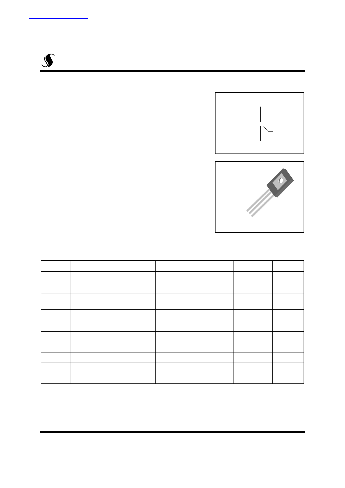
Symbol
TO-126
BT134-F
2.T2
○
▼
▲
○
3.Gate
○
1.T1
3
2
1
Absolute Maximum Ratings ( T
= 25°C unless otherwise specified )
J
Symbol Parameter Condition Ratings Units
V
DRM
I
T(RMS)
I
TSM
2
I
P
GM
P
G(AV)
I
GM
V
GM
T
T
STG
J
Repetitive Peak Off-State Voltage 600 V
= 104 °C
R.M.S On-State Current
Surge On-State Current
t
2
I
t
Peak Gate Power Dissipation 5 W
Average Gate Power Dissipation Over any 20ms period 0.5 W
Peak Gate Current 2 A
Peak Gate Voltage 5 V
Operating Junction Temperature - 40 ~ 125 °C
Storage Temperature - 40 ~ 150 °C
T
C
One Cycle, 50Hz/60Hz, Peak,
Non-Repetitive
t = 10ms 3.1
4A
25/27 A
2
A
s
Nov, 2003. Rev. 0
1/6
copyright@SemiWell Semiconductor Co., Ltd., All rights reserved.
Page 2
BT134-F
Electrical Characteristics
Symbol Items Conditions
V
= V
I
DRM
V
TM
+
I
GT1
-
I
GT1
-
I
GT3
+
I
GT3
+
V
GT1
-
V
GT1
-
V
GT3
+
V
GT3
V
GD
(dv/dt)c
Repetitive Peak Off-State
Current
Peak On-State Voltage
D
= 125 °C
T
J
= 5 A, Inst. Measurement
I
T
Ⅰ
Ⅱ ──
Gate Trigger Current
V
D
Ⅲ ──
Ⅳ ──
Ⅰ
Ⅱ ──
Gate Trigger Voltage
V
D
Ⅲ ──
Ⅳ ──
= 125 °C, VD = 1/2 V
Non-Trigger Gate Voltage
Critical Rate of Rise Off-State
Voltage at Commutation
T
J
T
= 125 °C, [di/dt]c = -0.75 A/ms,
J
V
D
, Single Phase, Half Wave
DRM
= 6 V, RL=10 Ω
= 6 V, RL=10 Ω
=2/3 V
DRM
DRM
Ratings
Min. Typ. Max.
──
──
──
──
0.2
5.0
──
──
0.5 mA
1.7 V
25
25
25
70
1.5
1.5
1.5
2.5
Unit
mA
V
V
V/㎲
2/6
R
I
H
th(j-c)
Holding Current
Thermal Impedance Junction to case
─
5
──
─
mA
3.5 °C/W
Page 3

Fig 1. Gate Characteristics Fig 2. On-State Voltage
BT134-F
1
10
VGK = 5V
PGK = 5W
P
= 0.5W
G(AV)
25℃
0
10
Gate Voltage [V]
=2A
GM
I
VGD = 0.2V
-1
10
1
10
2
10
Gate Current [mA]
3
10
Fig 3. On State Current vs.
Maximum Power Dissipation
7
θ
π
π
6
5
4
θ
θ
: Conduction Angle
2
360°
3
2
Power Dissipation [W]
1
0
012345
RMS On-State Current [A]
θ = 180
θ = 150
θ = 120
θ = 90
θ = 60
θ = 30
o
o
o
o
o
o
2
10
1
10
125 oC
0
10
On-State Current [A]
-1
10
0.51.01.52.02.53.0
25 oC
On-State Voltage [V]
Fig 4. On State Current vs.
Allowable Case Temperature
130
C]
o
120
o
θ
π
π
110
Allowable Case Temperature [
100
θ
θ
: Conduction Angle
012345
2
360°
RMS On -S ta t e Current [A]
θ = 30
θ = 60
θ = 90
θ = 120
θ = 150
θ = 180
o
o
o
o
o
Fig 5. Surge On-State Current Rating
( Non-Repetitive )
35
30
25
20
15
10
Surge On-State Current [A]
5
0
0
10
50Hz
10
60Hz
1
Time (cycles)
Fig 6. Gate Trigger Voltage vs.
Junction Temperature
10
C)
C)
o
o
(t
2
10
3
10
1
(25
GT
GT
V
V
0.1
-50 0 50 100 150
Junction Temperature [ oC]
3/6
Page 4

BT134-F
Fig 7. Gate Trigger Current vs.
Junction Temperature
10
C)
C)
o
o
1
(t
(25
GT
I
GT
I
0.1
-50 0 50 100 150
Junction Temperature [oC]
Fig 9. Gate Trigger Characteristics Test Circuit
Fig 8. Transient Thermal Impedance
-1
10
Time (sec)
0
10
1
10
2
10
1
10
C/W]
o
+
I
GT1
-
I
GT1
-
I
GT3
+
I
GT3
10
Transient Thermal Impedance [
0
10
-1
-3
10
-2
10
10Ω
6V
▼
▲
10Ω
▼
●
A
R
V
●
G
6V
▲
●
A
V
●
10Ω
▼
▲
6V
R
G
Test Procedure Ⅰ Test Procedure Ⅱ Test Procedure Ⅲ
4/6
10Ω
●
A
V
●
R
▼▲
●
6V
G
A
R
V
●
G
Test Procedure Ⅳ
Page 5

TO-126 Package Dimension
BT134-F
Dim.
Min. Typ. Max. Min. Typ. Max.
mm Inch
A 7.5 7.9 0.295 0.311
B 10.8 11.2 0.425 0.441
C 14.2 14.7 0.559 0.579
D 2.7 2.9 0.106 0.114
E 3.8 0.150
F 2.5 0.098
G 1.2 1.5 0.047 0.059
H 2.3 0.091
I 4.6 0.181
J 0.48 0.62 0.019 0.024
K 0.7 0.86 0.028 0.034
L 1.4 0.055
φ
3.2 0.126
A
B
F
3
C
2
1
D
E
φ
G
L
1. Gate
2. T2
3. T1
J
H
I
K
5/6
Page 6

TO-126 Package Dimension, Forming
BT134-F
Dim.
Min. Typ. Max. Min. Typ. Max.
mm Inch
A 7.5 7.9 0.295 0.311
B 10.8 11.2 0.425 0.441
C 14.2 14.7 0.559 0.579
D 2.7 2.9 0.106 0.114
E 3.8 0.150
F 2.5 0.098
G 1.2 1.5 0.047 0.059
H 2.3 0.091
I 4.6 0.181
J 0.48 0.62 0.019 0.024
K 0.7 0.86 0.028 0.034
L 1.4 0.055
M 5.0 0.197
φ
3.2 0.126
6/6
A
E
B
φ
F
3
C
2
1
M
D
G
L
1. Gate
2. T2
3. T1
J
H
I
K
 Loading...