

Page 1
HIGH SPEED SATURATED SWITCHES
DESCRIPTION
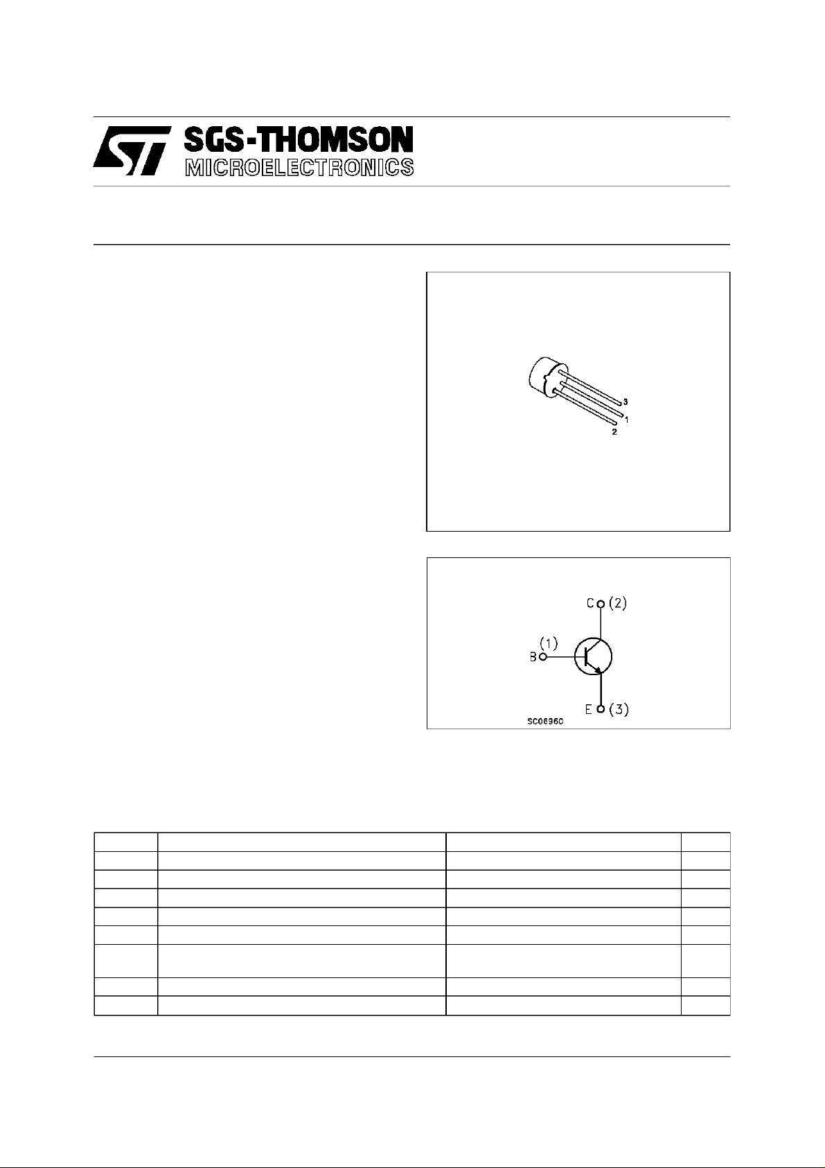
The BSX20 is a silicon planar epitaxial NPN
transistors in Jedec TO-18 metal case. They are
primarily intended for veeryhigh speed saturated
switchingapplications.
BSX20
TO-18
INTERNAL SCHEMATIC DIAGRAM
ABSOLUTE MAXIMUM RATINGS
Symb o l Parameter Val u e Uni t
V
V
V
V
P
T
Collector-Base Voltage (IE=0) 40 V
CBO
Collector-Emitter Voltage (VBE=0) 40 V
CES
Collector-Emitter Voltage (IB=0) 15 V
CEO
Emitter-Base Voltage (IC=0) 4.5 V
EBO
Collect or Current (t = 10 µs) 0.5 A
I
C
Total Diss ipat ion at T
tot
Stora ge Tem per ature -65 t o 200
stg
Max. Op er at i ng Junct ion Temperat u r e 200
T
j
at T
amb
case
≤ 25oC
≤ 25oC
0.36
1.2
W
W
o
C
o
C
November 1997
1/6
Page 2
BSX20
THERMAL DATA
R
thj-case
R
thj- amb
Ther mal Resist ance Junc tion-Case Max
Thermal Resistance Junction-Ambient Max
146
486
o
C/W
o
C/W
ELECTRICAL CHARACTERISTICS (T
=25oC unlessotherwisespecified)
case
Symbol Parameter Test Conditions Min. Typ. Max. Unit
I
CBO
I
CES
I
CEX
I
BEX
I
EBO
V
CER(sus )
Collector Cut-off
Current (I
E
=0)
Collector Cut-off
Current (V
BE
=0)
Collector Cut-off
Current (V
BE
=-3V)
Base C ut-o ff Current
=-3V)
(V
BE
Emit ter Cut-o f f C urr ent
=0)
(I
C
∗ Collec tor-Emitt er
=20V
V
CB
V
=20V T
CB
V
=15V T
CE
=40V
V
CE
V
=15V T
CE
V
=15V T
CE
V
= 4.5 V 10 µA
EB
I
=10mA 20 V
C
=150oC
amb
=55oC
amb
=55oC0.6µA
amb
=55oC0.6µA
amb
0.4
30
0.4
1
Sust aining V olt age
=10Ω)
(R
BE
V
(BR) CEO
∗ Collect or- E mitt er
I
=10mA 15 V
C
Break dow n Voltage
=0)
(I
B
V
∗ Collector-E m it t er
CE(sat)
Saturation Voltage
V
∗ Base-Emitt er
BE(sat )
Saturation Voltage
V
∗ Base-Emitt er O n
BE(on)
Volt age
∗ DC C ur rent G ain IC=10mA VCE=1V
h
FE
C
f
CBO
Tr ansition F r eque nc y IC=10mA VCE= 10 V 500 600 M Hz
T
Collector Base
IC=10mA IB=1mA
=100mA IB=10mA
I
C
=10mA IB=0.3mA
I
C
IC=10mA IB=1mA
=100mA IB=10mA
I
C
IC=30µAVCE=20V
= 100oC
T
amb
=100mA VCE=2V
I
C
I
=10mA VCE=1V
C
=-55oC
T
amb
IE=0 VCB=5V 4 pF
0.7 0.85
350 m V
40
20
20
0.25
0.6
0.3
1.5
60
Capacit a nc e
C
EBO
Emitt er Base
IC=0 VEB=1V 4.5 pF
Capacit a nc e
∗∗ Storage Tim e VCC=10V IC=10mA
t
s
∗∗ Turn-on T ime VCC=3V IC=10mA
t
on
t
∗∗ Turn-off Time VCC=3V IC=10mA
off
∗
Pulsed: Pulse duration = 300µs, duty cycle≤ 1%
∗∗ See test circuit
=-IB2=10mA
I
B1
I
=3mA
B1
=6V IC=100mA
V
CC
=40mA
I
B1
=3mA IB2=-1.5mA
I
B1
=6V IC=100mA
V
CC
=40mA IB2=-20mA
I
B1
613ns
12
7
18
21
µA
µA
µA
µA
V
V
V
V
V
ns
ns
ns
ns
2/6
Page 3

BSX20
Base-emitterSaturationVoltage.Collector-emitter SaturationVoltage
DCCurrent Gain
TransitionFrequency.
DC Current Gain
3/6
Page 4

BSX20
Test circuitfor tS.
4/6
Page 5

TO-18 MECHANICAL DATA
BSX20
DIM.
MIN. TYP. MAX. MIN. TYP. MAX.
A 12.7 0.500
B 0.49 0.019
D 5.3 0.208
E 4.9 0.193
F 5.8 0.228
G 2.54 0.100
H 1.2 0.047
I 1.16 0.045
L45
o
mm inch
o
45
G
I
H
DA
F
E
L
B
C
0016043
5/6
Page 6

BSX20
Information furnished is believed to be accurate and reliable. However,SGS-THOMSON Microelectronicsassumes no responsability for the
consequencesof use ofsuch informationnor for any infringement of patentsor other rights ofthirdparties whichmay results from its use. No
licenseisgranted by implicationor otherwise underany patent orpatentrights ofSGS-THOMSONMicroelectronics. Specifications mentioned
in this publicationare subject to change withoutnotice.This publication supersedes and replacesall information previously supplied.
SGS-THOMSONMicroelectronics productsare not authorized for useas criticalcomponents in lifesupportdevices or systems withoutexpress
writtenapproval of SGS-THOMSONMicroelectonics.
1997 SGS-THOMSONMicroelectronics- Printedin Italy - AllRights Reserved
Australia- Brazil-Canada- China - France - Germany - Italy - Japan -Korea-Malaysia- Malta- Morocco - The Netherlands -
Singapore- Spain- Sweden- Switzerland-Taiwan - Thailand - United Kingdom- U.S.A
SGS-THOMSONMicroelectronics GROUPOF COMPANIES
...
6/6
 Loading...