

Page 1
PNP Silicon Switching Transistors BSS 80
BSS 82
● High DC current gain
● Low collector-emitter saturation voltage
● Complementary types: BSS 79, BSS 81 (NPN)
Type Ordering Code
BSS 80 B
BSS 80 C
BSS 82 B
BSS 82 C
Marking
CHs
CJs
CLs
CMs
(tape and reel)
Q62702-S557
Q62702-S492
Q62702-S560
Q62702-S482
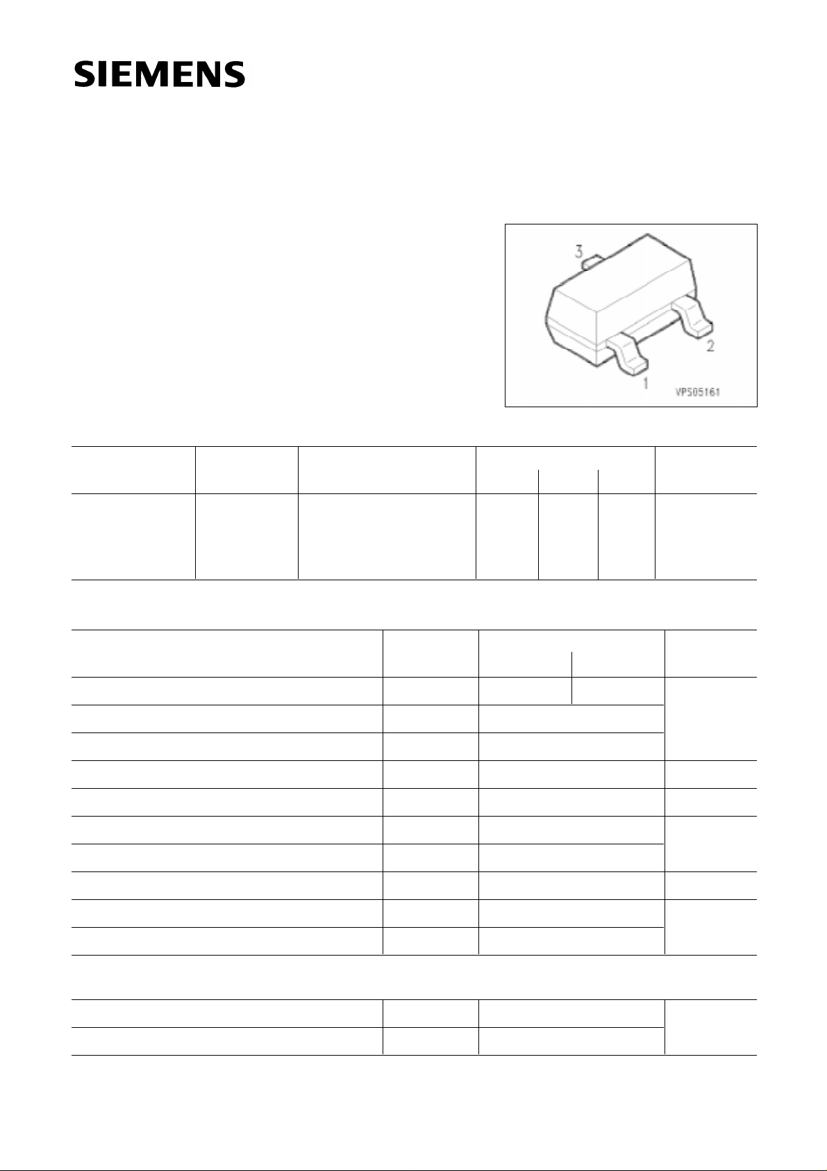
Pin Configuration
1 2 3
B E C
Package
SOT-23
Maximum Ratings
Parameter Symbol
BSS 80
Collector-emitter voltage V
CE0 40 V
Collector-base voltage VCB0
Emitter-base voltage VEB0
Collector current IC mA
Peak collector current I
Base current I
CM A
B mA
Peak base current IBM
Values
BSS 82
60
60
5
800
1
100
200
Unit
1)
Total power dissipation, T
Junction temperature T
Storage temperature range T
S =77 ˚C Ptot mW
j ˚C
stg – 65 … + 150
Thermal Resistance
Junction - ambient
2)
Junction - soldering point
1)
For detailed information see chapter Package Outlines.
2)
Package mounted on epoxy pcb 40 mm × 40 mm × 1.5 mm/6 cm2 Cu.
Semiconductor Group 1
Rth JA ≤ 290 K/W
th JS ≤ 220
R
330
150
5.91
Page 2
Electrical Characteristics
I
I
I
I
I
I
I
I
I
I
I
I
A = 25 ˚C, unless otherwise specified.
at T
DC characteristics
BSS 80
BSS 82
UnitValuesParameter Symbol
min. typ. max.
(BR)CE0
V
C = 10 mA BSS 80
BSS 82
V
Collector-base breakdown voltage
C = 10 µA
Emitter-base breakdown voltage
E = 10 µA
Collector-base cutoff current
CB = 50 V
V
CB = 50 V, TA = 150 ˚C
V
EB = 3 V
V
(BR)CB0 60 – –
V
(BR)EB0 5––
CB0
I
I
EB0 ––10
40
60
–
–
–
–
–
–
–
–
10
10
DC current gain
C = 100 µA, VCE = 10 V BSS 80 B/82 B
C = 1 mA, VCE = 10 V BSS 80 B/82 B
C = 10 mA, VCE = 10 V
1)
BSS 80 C/82 C
BSS 80 C/82 C
BSS 80 B/82 B
BSS 80 C/82 C
C = 150 mA, VCE = 10 V
1)
BSS 80 B/82 B
BSS 80 C/82 C
C = 500 mA, VCE = 10 V
1)
BSS 80 B/82 B
BSS 80 C/82 C
Collector-emitter saturation voltage
C = 150 mA, IB = 15 mA
C = 500 mA, IB = 50 mA
Base-emitter saturation voltage
C = 150 mA, IB = 15 mA
C = 500 mA, IB = 50 mA
1)
1)
VBEsat
40
75
40
100
40
100
40
100
40
50
–
–
–
–
–
–
–
–
–
–
–
–
–
–
–
–
–
–
–
–
–
–
–
–
120
300
–
–
0.4
1.6
1.3
2.6
VCollector-emitter breakdown voltage
nA
µA
nAEmitter-base cutoff current
–hFE
VVCEsat
1)
Pulse test conditions: t ≤ 300 µs, D = 2 %.
Semiconductor Group 2
Page 3

Electrical Characteristics
I
A = 25 ˚C, unless otherwise specified.
at T
AC characteristics
BSS 80
BSS 82
UnitValuesParameter Symbol
min. typ. max.
f
T – 250 –
C = 20 mA, VCE = 20 V, f = 100 MHz
C
obo –6–
CB = 10 V, f = 1 MHz
V
CC = 30 V, IC = 150 mA, IB1 = 150 mA
V
Delay time
Rise time
CC = 6 V, IC = 150 mA, IB1 = IB2 = 15 mA
V
Storage time
Fall time
d
t
tr
tstg
tf
–
–
–
–
–
–
–
–
Test circuits
Delay and rise time Storage and fall time
10
40
80
30
MHzTransition frequency
pFOpen-circuit output capacitance
ns
ns
ns
ns
Semiconductor Group 3
Page 4

BSS 80
BSS 82
Total power dissipation Ptot = f (TA*; TS)
* Package mounted on epoxy
Collector-base capacitance Ccb = f (VCB)
f = 1 MHz
Permissible pulse load P
tot max/Ptot DC = f (tp)
Transition frequency f
CE = 20 V
V
T = f (IC)
Semiconductor Group 4
Page 5

BSS 80
BSS 82
Saturation voltage IC = f (VBE sat, VCE sat)
FE =10
h
Delay time td = f (IC)
Rise time t
r = f (IC)
Storage time t
stg = f (IC)
Fall time t
f = f (IC)
Semiconductor Group 5
Page 6

DC current gain hFE = f (IC)
CE =10V
V
BSS 80
BSS 82
Semiconductor Group 6
 Loading...