

Page 1
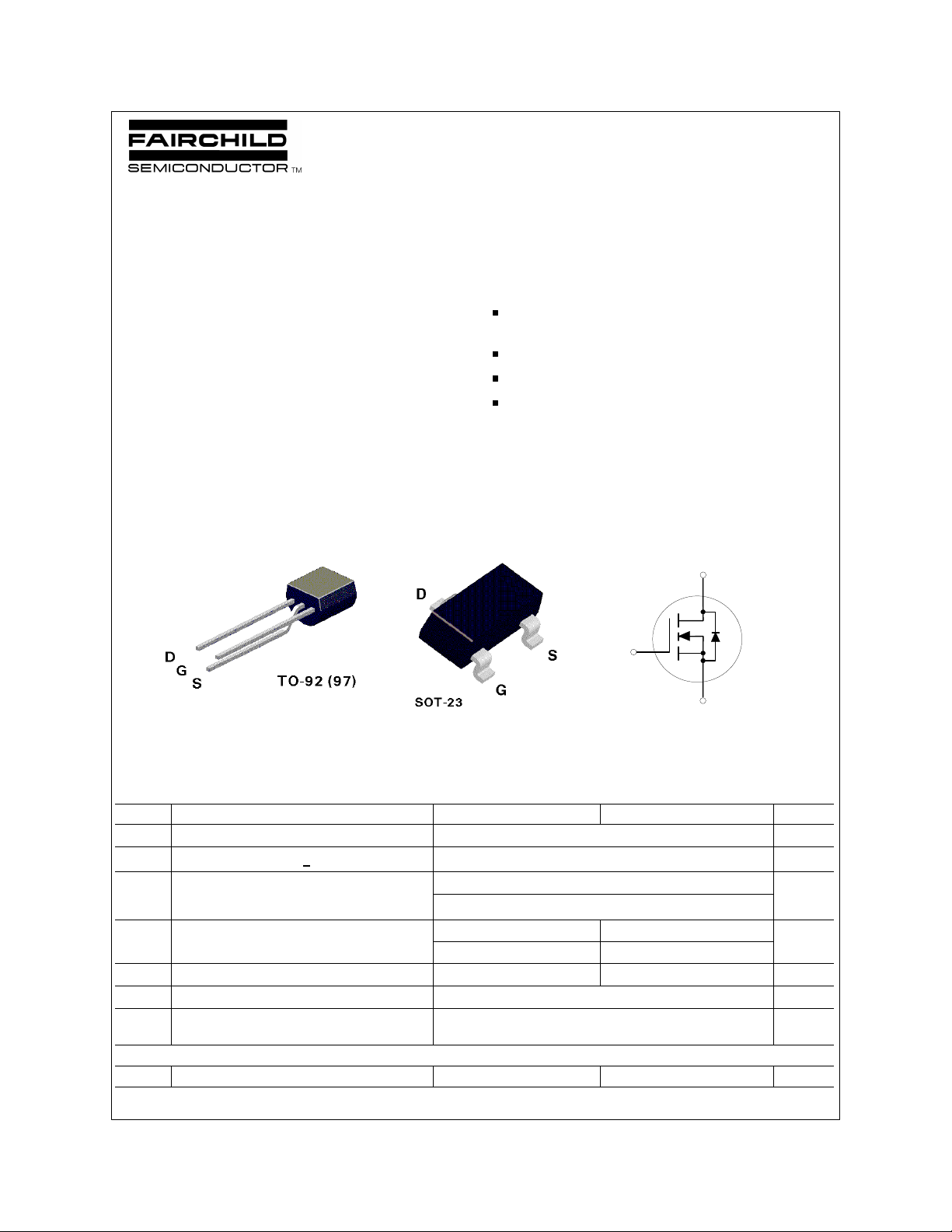
September 1996
BSS100 / BSS123
N-Channel Logic Level Enhancement Mode Field Effect Transistor
General Description Features
These N-Channel logic level enhancement mode power
field effect transistors are produced using Fairchild's
proprietary, high cell density, DMOS technology. This
very high density process has been especially tailored to
minimize on-state resistance, provide superior switching
performance. This product is particularly suited to low
voltage, low current applications, such as small servo
motor controls, power MOSFET gate drivers, and other
switching applications.
_______________________________________________________________________________
BSS100: 0.22A, 100V. R
BSS123: 0.17A, 100V. R
DS(ON)
DS(ON)
= 6Ω @ V
= 6Ω @ V
GS
GS
High density cell design for extremely low R
Voltage controlled small signal switch.
Rugged and reliable.
D
= 10V.
= 10V
DS(ON)
.
G
BSS100
Absolute Maximum Ratings T
BSS123
= 25°C unless otherwise noted
A
S
Symbol Parameter BSS100 BSS123 Units
V
DSS
V
DGR
V
GSS
I
D
Drain-Source Voltage 100 V
Drain-Gate Voltage (RGS < 20KΩ)
100 V
Gate-Source Voltage - Continuous ± 14 V
- Non Repetitive (TP < 50 µS)
± 20
Drain Current - Continuous 0.22 0.17 A
- Pulsed 0.9 0.68
P
TJ,T
T
D
L
Total Power Dissipation @ TA = 25°C 0.63 0.36 W
Operating and Storage Temperature Range -55 to 150 °C
STG
Maximum Lead Temperature for Soldering
300 °C
Purposes, 1/16" from Case for 10 Seconds
THERMAL CHARACTERISTICS
R
JA
θ
Thermal Resistacne, Junction-to-Ambient 200 350 °C/W
© 1997 Fairchild Semiconductor Corporation
BSS100 Rev. F1 / BSS123 Rev. F1
Page 2
Electrical Characteristics (T
= 25°C unless otherwise noted)
A
Symbol Parameter Conditions Type Min Typ Max Units
OFF CHARACTERISTICS
BV
I
DSS
I
GSSF
DSS
Drain-Source Breakdown Voltage VGS = 0 V, ID = 250 µA All 100 V
Zero Gate Voltage Drain Current VDS = 100 V, V
VDS = 100 V, V
VDS = 100 V, V
VDS = 60 V, V
VDS = 20 V, V
= 0 V
GS
= 0 V
GS
= 0 V TJ=125oC All 60 µA
GS
= 0 V
GS
= 0 V
GS
Gate - Body Leakage, Forward VGS = 20 V, VDS = 0 V
VGS = 20 V, VDS = 0 V
BSS100
BSS123
BSS100
BSS123
BSS100
BSS123
15 µA
1 µA
10 nA
10 nA
10 nA
50 nA
ON CHARACTERISTICS (Note 1)
V
R
g
GS(th)
DS(ON)
FS
Gate Threshold Voltage VDS = VGS, ID = 1 mA All 0.8 1.4 2 V
Static Drain-Source On-Resistance VGS = 10 V, ID = 0.22 A
VGS = 10 V, ID = 0.17 A
VGS = 4.5 V, ID = 0.22 A
VGS = 4.5 V, ID = 0.17 A
Forward Transconductance VDS = 10 V, ID = 0.22 A
VDS = 10 V, ID = 0.17 A
BSS100
BSS123
BSS100
BSS123
BSS100
BSS123
2.8 6
2.8 6
3.2 10
3.2 10
0.08 0.4 S
0.08 0.4
DYNAMIC CHARACTERISTICS
C
iss
C
oss
C
rss
Input Capacitance VDS = 25 V, VGS = 0 V,
Output Capacitance All 10 15 pF
f = 1.0 MHz
All 29 60 pF
Reverse Transfer Capacitance All 2 6 pF
SWITCHING CHARACTERISTICS (Note 1)
t
t
t
t
Q
Q
Q
D(on)
r
D(off)
f
g
gs
gd
Turn - On Delay Time VDD = 30 V, ID = 0.28 A,
Turn - On Rise Time All 8 ns
VGS = 10 V, R
GEN
= 50 Ω
All 8 ns
Turn - Off Delay Time All 13 ns
Turn - Off Fall Time All 16 ns
Totall Gate Charge VDS = 10 V, ID = 0.22 A,
Gate-Source Charge All 0.15 0.25 nC
VGS = 10 V,
All 1.4 2 nC
Gate-Drain Charge All 0.2 0.4 nC
DRAIN-SOURCE DIODE CHARACTERISTICS AND MAXIMUM RATINGS
I
S
I
SM
V
SD
Note:
1. Pulse Test: Pulse Width < 300 µs, Duty Cycle < 2.0%.
Maximum Continuous Source Current
Maximum Pulse Source Current (Note 1)
Drain-Source Diode Forward Voltage VGS = 0 V, IS = 0.44 A
VGS = 0 V, IS = 0.34 A
BSS100
BSS123
BSS100
BSS123
BSS100
BSS123
0.22 A
0.17
0.9 A
0.68
0.9 1.3 V
0.9 1.3
Ω
BSS100 Rev. F1 / BSS123 Rev. F1
Page 3
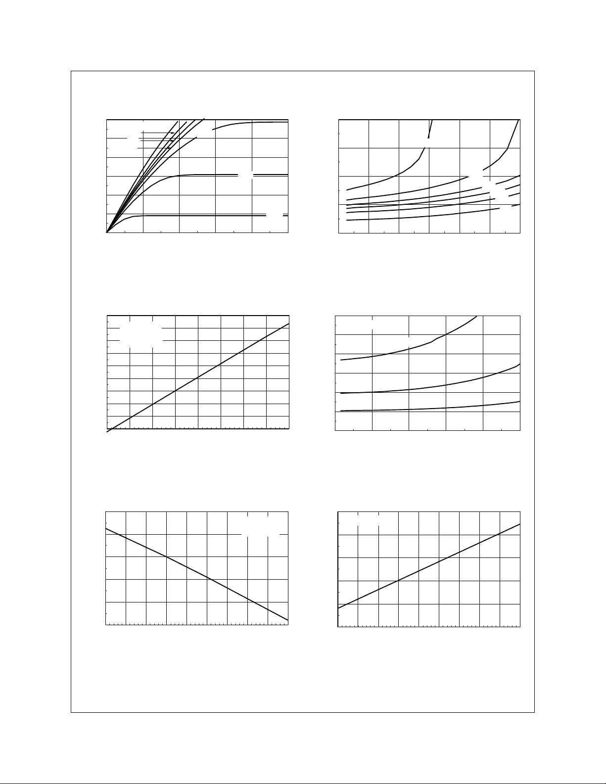
Typical Electrical Characteristics
0.6
0.5
0.4
0.3
0.2
0.1
D
I , DRAIN-SOURCE CURRENT (A)
0
0 1 2 3 4 5
V =10V
GS
5.0
4.0
3.5
V , DRAIN-SOURCE VOLTAGE (V)
DS
3.0
2.5
2.0
2.4
V =2.5V
2
1.6
DS(on)
R , NORMALIZED
1.2
DRAIN-SOURCE ON-RESISTANCE
0.8
0 0.1 0.2 0.3 0.4 0.5 0.6
GS
I , DRAIN CURRENT (A)
D
Figure 1. On-Region Characteristics. Figure 2. On-Resistance Variation with Gate
Voltage and Drain Current.
2.2
2
I = 220mA
D
V =10V
1.8
1.6
1.4
1.2
DS(ON)
R , NORMALIZED
0.8
DRAIN-SOURCE ON-RESISTANCE
0.6
0.4
GS
1
-50 -25 0 25 50 75 100 125 150
T , JUNCTION TEMPERATURE (°C)
J
3
V = 10V
2.5
1.5
DS(on)
R , NORMALIZED
0.5
DRAIN-SOURCE ON-RESISTANCE
GS
T = 125°C
J
2
25°C
1
0
0 0.2 0.4 0.6 0.8 1
I , DRAIN CURRENT (A)
D
3.0
-55°C
3.5
4.0
5.0
10
Figure 3. On-Resistance Variation
with Temperature.
1.2
V = V
DS
I = 250µA
1.1
1
0.9
th
V , NORMALIZED
0.8
GATE-SOURCE THRESHOLD VOLTAGE
0.7
-50 -25 0 25 50 75 100 125 150 175
T , JUNCTION TEMPERATURE (°C)
J
D
Figure 5. Gate Threshold Variation with
Temperature.
Figure 4. On-Resistance Variation with Drain
Current and Temperature.
1.15
I = 250µA
GS
DSS
BV , NORMALIZED
D
1.1
1.05
1
0.95
DRAIN-SOURCE BREAKDOWN VOLTAGE
0.9
-50 -25 0 25 50 75 100 125 150 175
T , JUNCTION TEMPERATURE (°C)
J
Figure 6. Breakdown Voltage Variation with
Temperature.
BSS100 Rev. F1 / BSS123 Rev. F1
Page 4

Typical Electrical Characteristics (continued)
80
50
20
10
5
CAPACITANCE (pF)
f = 1 MHz
V = 0V
GS
1
0.1 0.2 0.5 1 2 5 10 50
V , DRAIN TO SOURCE VOLTAGE (V)
DS
C
C
iss
oss
C
rss
10
I =220mA
D
8
6
4
2
GS
V , GATE-SOURCE VOLTAGE (V)
0
0 0.2 0.4 0.6 0.8 1 1.2 1.4
Q , GATE CHARGE (nC)
g
V = 5V
Figure 7. Capacitance Characteristics. Figure 8. Gate Charge Characteristics.
0.8
V = 5V
DS
0.6
0.4
0.2
T = -55°C
J
25°C
125°C
DS
20
FS
g , TRANSCONDUCTANCE (SIEMENS)
0
0 0.1 0.2 0.3 0.4 0.5 0.6
I , DRAIN CURRENT (A)
D
Figure 9. Transconductance Variation with Drain
Current and Temperature.
V
DD
V
IN
R
L
D
V
GS
R
GEN
G
DUT
S
Figure 10. Switching Test Circuit.
V
OUT
t t
on off
t
d(on)
t
r
90%
V
OUT
V
IN
10%
50%
10%
PULSE WIDTH
Figure 11. Switching Waveforms.
t
d(off)
50%
90%
90%
10%
t
f
INVERTED
BSS100 Rev. F1 / BSS123 Rev. F1
Page 5

t , TIME (sec)
TRANSIENT THERMAL RESISTANCE
2
t , TIME (sec)
TRANSIENT THERMAL RESISTANCE
1
0.5
RDS(ON) Limit
0.2
0.1
0.05
D
I , DRAIN CURRENT (A)
0.01
0.005
V = 20V
GS
SINGLE PULSE
T = 25°C
A
1 5 10 20 50 100 150
V , DRAIN-SOURCE VOLTAGE (V)
DS
DC
10s
10ms
100ms
1s
1ms
100us
2
1
0.5
RDS(ON) Limit
0.2
0.1
0.05
D
I , DRAIN CURRENT (A)
0.01
0.005
V = 20V
GS
SINGLE PULSE
T = 25°C
A
1 5 10 20 50 100 150
V , DRAIN-SOURCE VOLTAGE (V)
DS
DC
10s
10ms
100ms
1s
100us
1ms
Figure 12. BSS100 Maximum Safe
Operating Area.
Figure 13. BSS123 Maximum Safe
Operating Area.
1
0.5
0.2
0.1
0.05
r(t), NORMALIZED EFFECTIVE
0.02
0.01
D = 0.5
R (t) = r(t) * R
θ
JA
R = 200 C/W
θ
JA
P(pk)
t
1
t
2
T - T = P * R (t)
J
A
Duty Cycle, D = t /t
0.05
0.02
0.01
0.2
0.1
Single Pulse
0.0001 0.001 0.01 0.1 1 10 100 300
1
Figure 14. BSS100 Transient Thermal Response Curve.
1
D = 0.5
0.5
0.2
0.2
0.1
0.1
0.05
0.05
0.02
0.01
r(t), NORMALIZED EFFECTIVE
0.01
Single Pulse
0.002
0.001
0.0001 0.001 0.01 0.1 1 10 100 300
1
R (t) = r(t) * R
θ
JA
R = 347 C/W
θ
JA
P(pk)
t
1
t
2
T - T = P * R (t)
J
A
Duty Cycle, D = t /t
o
θ
θ
JA
o
θ
JA
1 2
θ
JA
JA
1 2
Figure 15. BSS123 Transient Thermal Response Curve.
BSS100 Rev. F1 / BSS123 Rev. F1
Page 6

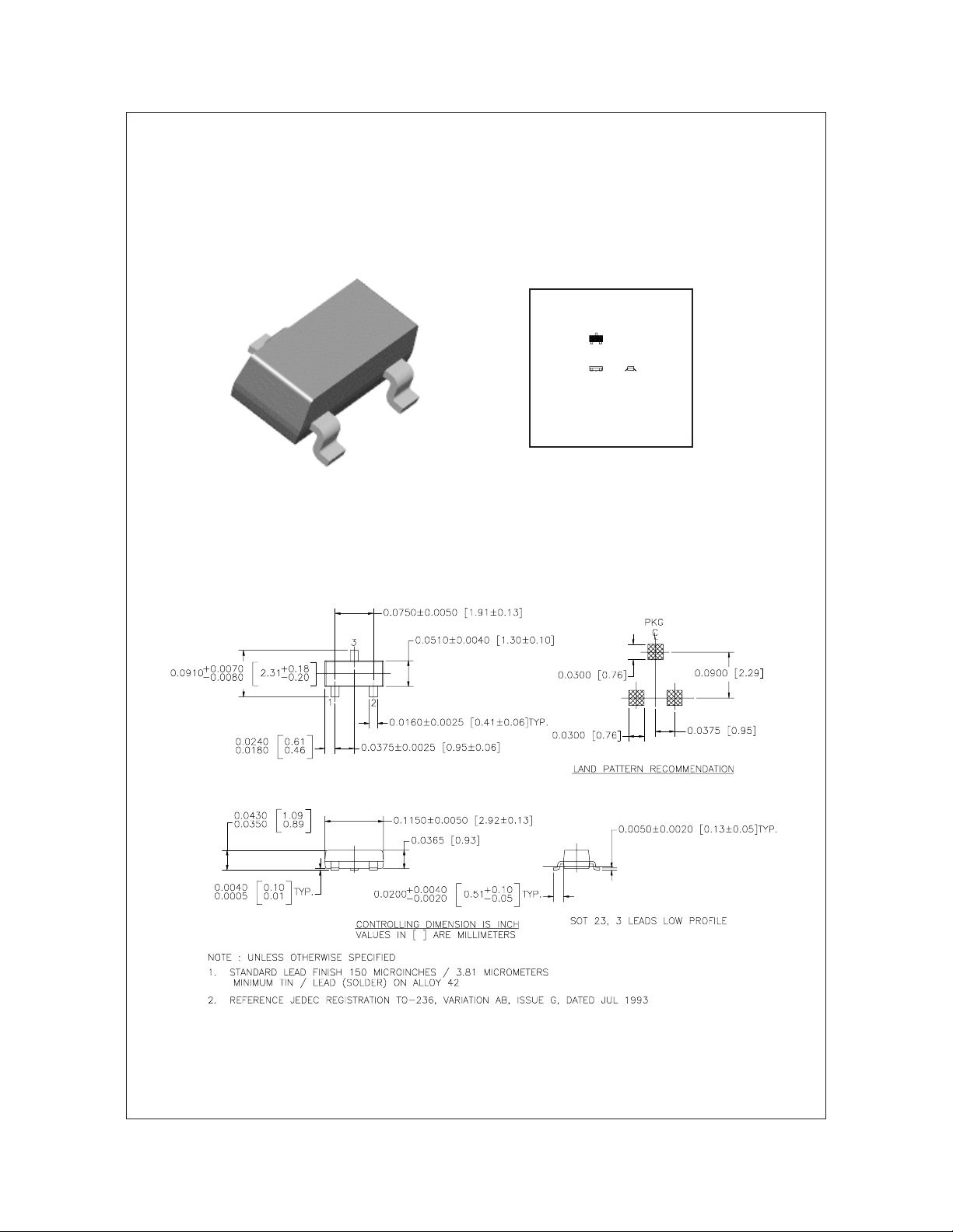
TO-92 Package Dimensions
TO-92; TO-18 Reverse Lead Form (J35Z Option)
(FS PKG Code 92, 94, 96)
1:1
Scale 1:1 on letter size paper
Dimensions shown below are in:
inches [millimeters]
Part Weight per unit (gram): 0.22
;
*
*
Note: All package 97 or 98 transistors are leadformed
to this configuration prior to bulk shipment. Order
L34Z option if in-line leads are preferred on package
97 or 98.
* Standard Option on 97 & 98 package code
January 2000, Rev. B
Page 7

SOT-23 Tape and Reel Data and Package Dimensions
SOT-23 Packagin g
Configu ration: Figur e 1.0
SOT-23 Packaging Information
Packaging Option
Packaging type
Qty per Reel/Tube/Bag
Reel Size
Box Dimension (mm )
Max qty per B o x
Weight per unit (gm)
Weight per Reel (kg)
Note/Comments
Customized Label
Stan dard
(no flow code)
3,000 10,000
7" Dia
187x107x183 34 3x34 3x64
24,000 30,000
0.0082 0.0082
0.1175 0.4006
TNR
D87Z
TNR
13"
Antistatic Cover Tape
Human Readable
Label
Embossed
Carrier Tape
343mm x 342mm x 64mm
Intermediate box for L87Z Option
Packaging Description:
SOT-23
parts are shipped in tape. The carrier tape is
made from a dissipative (carbon filled) polycarbonat e
resin. The cover tape is a multilayer film (Heat Activated
Adhesive in nature) primaril y composed of polyester film,
adhesive layer, sealant, and anti-static sprayed agent.
These reeled parts i n standard option are shipped with
3,000 uni ts per 7" or 177cm diameter reel. The reels are
dark blue in color and is made of polystyrene plastic (antistatic coated). Other option comes in 10,000 units per 13"
or 330cm diameter reel. This and some other opt i ons are
described in the Packaging Information table.
These full reels are individually labeled and placed insi de
a standard intermediat e made of recyclable corrugated
brown paper with a Fairchil d logo printing. One pizza box
contains eight reels max imum. And these intermediate
boxes are placed inside a labeled shipping box which
comes in diff erent sizes dependin g on the number of parts
shipped.
3P 3P 3P 3P
SOT-23 Unit Orientation
Human Readable Label
Human Readable Label sample
SOT-23 Tape Leader and Trailer
Configuration: Figur e 2.0
Carrier Tape
Cover Tape
Trailer Tape
300mm minimum or
75 empty pockets
Components
Human readable
Label
187mm x 107mm x 183mm
Intermediate Box for Standard Option
Leader Tape
500mm minimum or
125 empty pockets
September 1999, Rev. C
Page 8

SOT-23 Tape and Reel Data and Package Dimensions, continued
SOT-23 Embossed Carrier Tape
Confi guration: Figure 3.0
T
B0
Wc
D0P0 P2
D1
E1
W
F
E2
Tc
K0
P1
A0
User Direction of Feed
Dimensions are in millimeter
Pkg type
SOT-23
(8mm)
Notes: A0, B0, and K0 dimensions are determined with respect to the EIA/Jedec RS-481
SOT-23 Reel Configuration: Figure 4.0
A0 B0 W D0 D1 E1 E2 F P1 P0 K0 T Wc Tc
3.15
2.77
8.0
1.55
1.125
1.75
6.25
+/-0.10
+/-0.10
+/-0.3
+/-0.05
+/-0.125
+/-0.10
3.50
min
+/-0.05
rotational and lateral movement requirements (see sketches A, B, and C).
20 deg maximum
B0
20 deg maximum component rotation
Sketch A (Side or Fro nt Sectional View)
Component Rotation
W1 Measured at Hub
A0
Sketch B (Top View)
Component Rotation
4.0
+/-0.1
Typical
component
cavity
center line
Typical
component
center line
Dim A
Max
4.0
+/-0.1
1.30
0.228
+/-0.013
5.2
+/-0.3
0.5mm
maximum
+/-0.10
0.5mm
maximum
Sketch C (Top View)
Component lateral movement
0.06
+/-0.02
Dim A
max
Tape Size
8mm 7" Dia
8mm 13" Dia
Reel
Option
Dim N
Diameter Option
7"
See detail AA
B Min
Dim C
13" Diameter Option
See detail AA
W2 max Measured at Hub
W3
Dim D
min
DETAIL AA
Dimensions are in inches and millimeters
Dim A Dim B Dim C Dim D Dim N Dim W1 Dim W2 Dim W3 (LSL-USL)
7.00
0.059
177.8
13.00
330
1.5
0.059
1.5
512 +0.020/-0.008
13 +0.5/-0.2
512 +0.020/-0.008
13 +0.5/-0.2
0.795
2.165550.331 +0.059/-0.000
20.2
0.795
4.00
20.2
100
8.4 +1.5/0
0.331 +0.059/-0.000
8.4 +1.5/0
0.567
14.4
0.567
14.4
0.311 – 0.429
7.9 – 10.9
0.311 – 0.429
7.9 – 10.9
September 1999, Rev. C
Page 9
SOT-23 Tape and Reel Data and Package Dimensions, continued
SOT-23 (FS PKG Code 49)
1:1
Scale 1:1 on letter size paper
Dimensions shown below are in:
inches [millimeters]
Part Weight per unit (gr am): 0.0082
September 1998, Rev. A1
Page 10

TRADEMARKS
The following are registered and unregistered trademarks Fairchild Semiconductor owns or is authorized to use and is
not intended to be an exhaustive list of all such trademarks.
ACEx™
CoolFET™
CROSSVOLT™
2
CMOS
E
TM
FACT™
FACT Quiet Series™
®
FAST
FASTr™
GTO™
HiSeC™
ISOPLANAR™
MICROWIRE™
POP™
PowerTrench
QFET™
QS™
Quiet Series™
SuperSOT™-3
SuperSOT™-6
SuperSOT™-8
SyncFET™
TinyLogic™
UHC™
VCX™
DISCLAIMER
FAIRCHILD SEMICONDUCTOR RESERVES THE RIGHT TO MAKE CHANGES WITHOUT FURTHER
NOTICE TO ANY PRODUCTS HEREIN TO IMPROVE RELIABILITY, FUNCTION OR DESIGN. FAIRCHILD
DOES NOT ASSUME ANY LIABILITY ARISING OUT OF THE APPLICA TION OR USE OF ANY PRODUCT
OR CIRCUIT DESCRIBED HEREIN; NEITHER DOES IT CONVEY ANY LICENSE UNDER ITS PATENT
RIGHTS, NOR THE RIGHTS OF OTHERS.
LIFE SUPPORT POLICY
FAIRCHILD’S PRODUCTS ARE NOT AUTHORIZED FOR USE AS CRITICAL COMPONENTS IN LIFE SUPPORT
DEVICES OR SYSTEMS WITHOUT THE EXPRESS WRITTEN APPROV AL OF FAIRCHILD SEMICONDUCTOR CORPORA TION.
As used herein:
1. Life support devices or systems are devices or
systems which, (a) are intended for surgical implant into
the body, or (b) support or sustain life, or (c) whose
failure to perform when properly used in accordance
with instructions for use provided in the labeling, can be
reasonably expected to result in significant injury to the
user.
2. A critical component is any component of a life
support device or system whose failure to perform can
be reasonably expected to cause the failure of the life
support device or system, or to affect its safety or
effectiveness.
PRODUCT STA TUS DEFINITIONS
Definition of Terms
Datasheet Identification Product Status Definition
Advance Information
Preliminary
No Identification Needed
Obsolete
Formative or
In Design
First Production
Full Production
Not In Production
This datasheet contains the design specifications for
product development. Specifications may change in
any manner without notice.
This datasheet contains preliminary data, and
supplementary data will be published at a later date.
Fairchild Semiconductor reserves the right to make
changes at any time without notice in order to improve
design.
This datasheet contains final specifications. Fairchild
Semiconductor reserves the right to make changes at
any time without notice in order to improve design.
This datasheet contains specifications on a product
that has been discontinued by Fairchild semiconductor.
The datasheet is printed for reference information only.
Rev. D
 Loading...