

Page 1
Smart Lowside Power Switch
)
)
)
HITFET® BSP 75
Features
•
Logic Level Input
•
Input protection (ESD)
•
Thermal shutdown (with restart)
•
Overload protection
•
Short circuit protection
•
Overvoltage protection
•
Current limitation
Product Summary
Continuous drain source voltage V
On-state resistance
Current limitation
Nominal load current
Clamping energy
DS
R
DS(ON
I
D(lim
I
D(Nom
E
AS
55 V
550
mΩ
1A
0.7 A
550 mJ
Application
•
All kinds of resistive, inductive and capacitive loads in switching applications
•
µC compatible power switch for 12 V and 24 V DC applications
•
Replaces electromechanical relays and discrete circuits
General Description
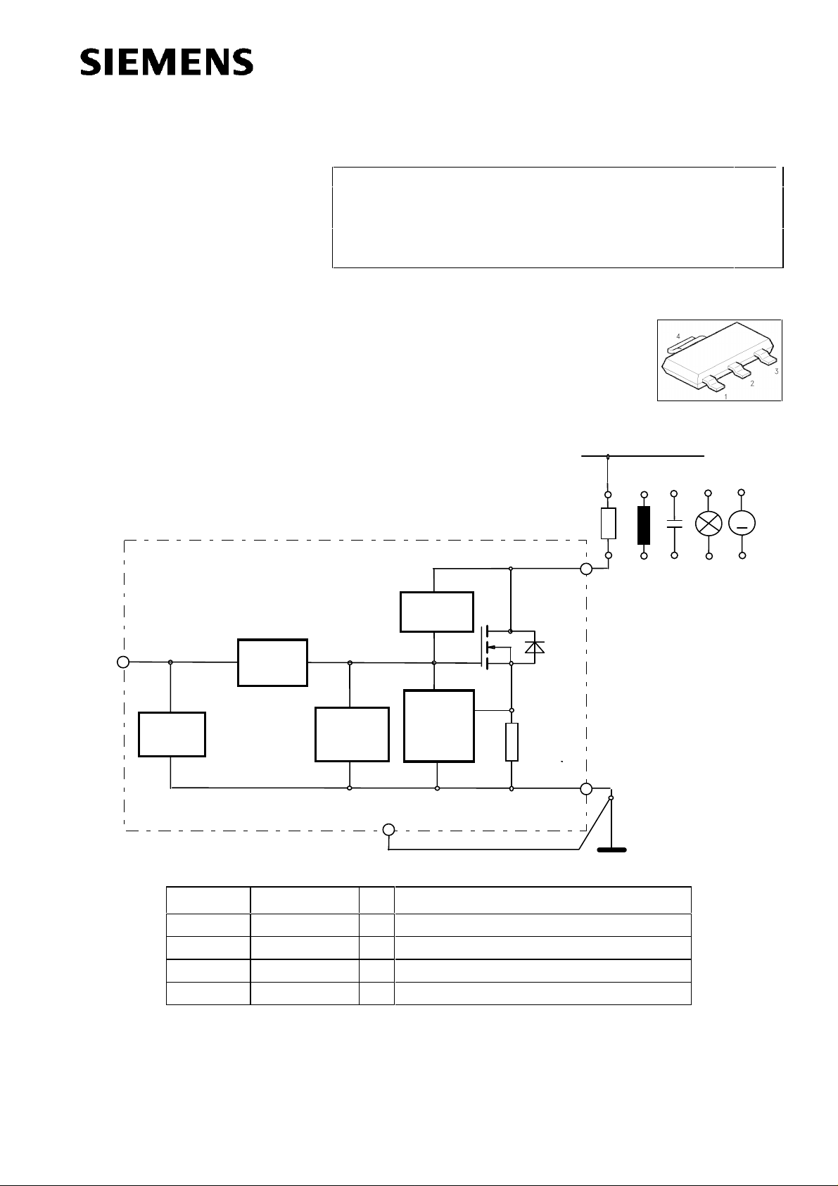
N channel vertical power FET in Smart Power Technology. Fully protected by embedded protection functions.
V
bb
+
LOAD
M
Drain
Overvoltage
protection
1
IN
ESD
Pin Symbol Function
1 IN Input
2 DRAIN Output to the load
3 SOURCE Ground
TAB SUBSTRATE Must be connected to Pin 3
dv/dt
limitation
Over-
temperature
protection
4
Short circuit
protection
Short circuit
Current
protection
limitation
Source
HITFET
2
3
Semiconductor Group Page 1 of 9 1998-02-04
Page 2
HITFET® BSP 75
)
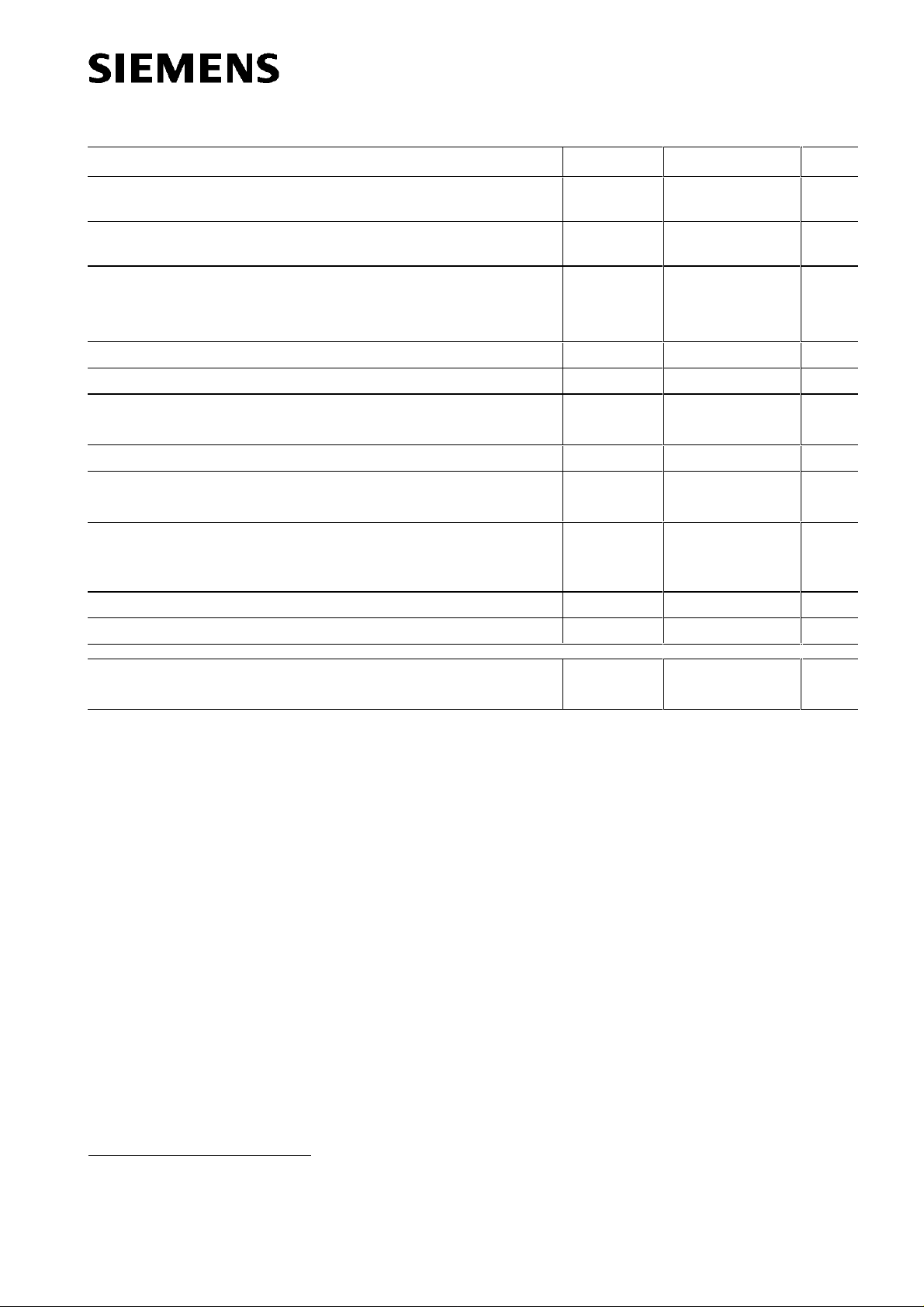
Maximum Ratings at Tj=25°C unless otherwise specified
Parameter Symbol Values Unit
Continuous drain source voltage
(overvoltage protection see page 4)
Drain source voltage for
short circuit protection
Load dump protection
1
)
R
I
R
=2 Ω;
I
=2 Ω;
t
=400ms; IN=low or high (8V)
d
t
=400ms; IN=high (8V)
d
V
LoadDump
=
U
+
U
;
U
S
=13.5 V
P
R
R
L
L
=50 Ω
=22 Ω
P
Continuous input voltage
Peak input voltage
Operating temperature range
Storage temperature range
Power dissipation (DC)
Unclamped single pulse inductive energy
I
D(ISO
= 0.7 A
Electrostatic discharge voltage (Human Body Model)
according to MIL STD 883D, method 3015.7 and
EOS/ESD assn. standard S5.1 - 1993
DIN humidity category, DIN 40 040 E
IEC climatic category, DIN IEC 68-1 40/150/56
V
DS
V
DS
V
LoadDump
V
IN
V
IN
T
j
T
stg
P
tot
E
AS
V
ESD
55 V
32 V
2
)
V
80
47
-0.2 ... +10 V
-0.2 ... +20 V
-40 ...+150
°C
-55 ...+150
1.8 W
550 mJ
4000 V
Thermal resistance junction soldering point:
junction - ambient
3
R
thJS
)
:
R
thJA
≤10
≤70
K/W
1
)
R
=internal resistance of the load dump test pulse generator LD200
I
2
)
V
LoadDump
3
)
Device on epoxy pcb 40mm x 40 mm x 1.5mm with 6cm
is setup without DUT connected to the generator per ISO 7637-1 and DIN 40 839.
2
copper area for pin 4 connection
Semiconductor Group Page 2 1998-02-04
Page 3
HITFET® BSP 75
V
V
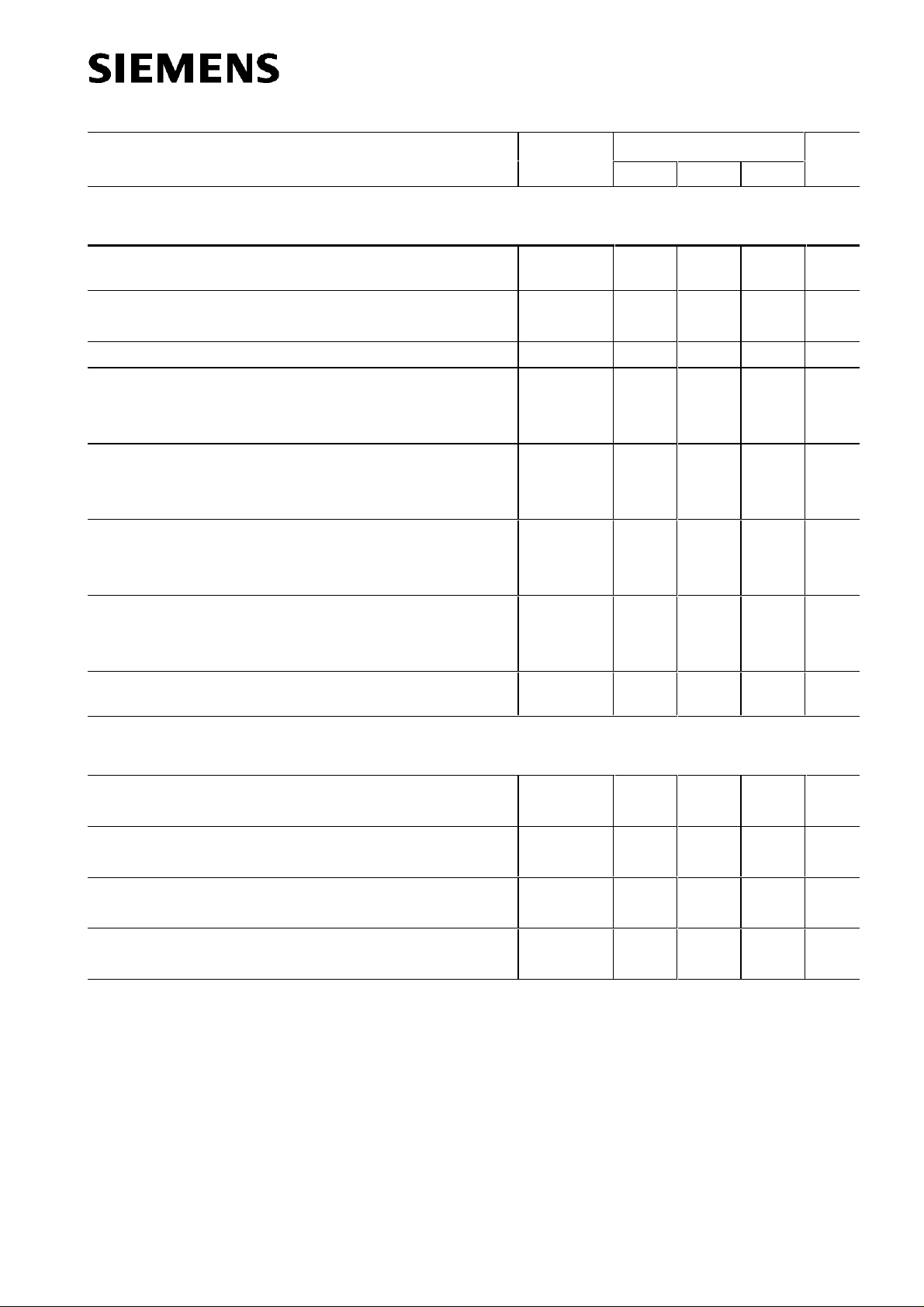
Electrical Characteristics
Parameter and Conditions Symbol Values Unit
at Tj = 25 °C, unless otherwise specified
Static Characteristics
min typ max
Drain source clamp voltage
I
= 10 mA
D
T
=-40...+150°C:
j
Off state drain current
V
= 0 V,
IN
Input threshold voltage
Input current normal operation,
V
IN = 5 V current limitation mode, ID=ID(lim):
V
DS
= 32 V
I
= 10 mA
D
T
=-40...+150°C:
j
I
D<ID(lim):
after thermal shutdown,
On-state resistance
ID = 0.7 A, V
IN
= 5 V
T
j
T
=150°C:
j
On-state resistance
ID = 0.7 A, V
= 10 V
IN
T
j
T
=150°C:
j
Nominal load current
V
= 12 V,
BB
T
j < 150°C
V
= 0.5 V,
DS
T
= 85°C
S
Current limit
= 10 V,
IN
= 12 V
DS
I
D=0 A:
=25°C:
=25°C:
V
DS(AZ)
I
DSS
V
IN(th)
I
IN(1)
I
IN(2)
I
IN(3)
R
DS(on)
R
DS(on)
I
D(Nom)
I
D(lim)
55 -- 70 V
-- -- 5 µA
2 2.5 3 V
--
1000
100
--
200
1500
--
550
--
850
--
475
--
750
200
300
2000
675
1350
550
1000
0.7 -- -- A
1 1.5 1.9 A
µA
mΩ
mΩ
Dynamic characteristics
Turn-on time
R
= 22 Ω, VIN= 0 to 10 V, Vbb= 12 V
L
Turn-off time
R
= 22 Ω, VIN= 10 to 0 V, Vbb= 12 V
L
V
to 90%
IN
V
to 10%
IN
I
D
I
D
Slew rate on 70 to 50% Vbb:
R
= 22 Ω, V
L
= 0 to 10 V, V
IN
bb
= 12 V
Slew rate off 50 to 70% Vbb:
R
= 22 Ω, VIN= 10 to 0 V, Vbb= 12 V
L
:
t
on
:
t
off
-d
V
/dt
DS
on
d
V
/dt
DS
off
-- 10 20 µs
-- 10 20 µs
-- 4 10 V/µs
-- 4 10 V/µs
Semiconductor Group Page 3 1998-02-04
Page 4
HITFET® BSP 75
)
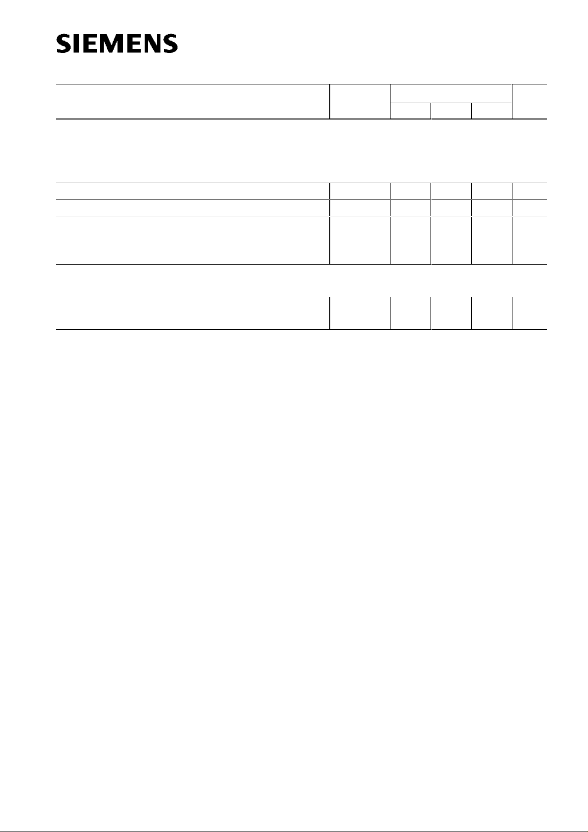
Parameter and Conditions Symbol Values Unit
at Tj = 25 °C, unless otherwise specified
Protection Functions
Thermal overload trip temperature
Thermal hysteresis ∆
Unclamped single pulse inductive energy
I
D(ISO
=0.7 A, Vbb=32 V Tj=25 °C
Tj=150 °C
Inverse Diode
Continuous source drain voltage
V
IN = 0 V,
-I
= 2*0.7 A
D
T
E
V
jt
T
AS
SD
jt
min typ max
150 165 -- °C
-- 10 -- K
550
200
--
--
--
mJ
--
-- 1 -- V
Circuit Description
The BSP 75 is a monolithic power switch in Smart Power Technology (SPT) with a logic level
input, an open drain DMOS output stage and integrated protection functions. It is designed
for all kind of resistive and inductive loads (relays, solenoid) in automotive and industrial applications.
Protection functions
• Overvoltage protection: An internal clamp limits the output voltage at V
63 V) when inductive loads are switched off.
• Current limitation: By means of an internal current measurement the drain current is lim-
ited at I
(1.4 - 1.5 A typ.). If the current limitation is active the device operates in the
D(lim)
linear region, so power dissipation may exceed the capability of the heatsink. This operation leads to an increasing junction temperature until the overtemperature threshold is
reached.
• Overtemperature and short circuit protection: This protection is based on sensing the
chip temperature. The location of the sensor ensures a fast and accurate junction temperature detection. Overtemperature shutdown occurs at minimum 150 °C. A hysteresis of
typ. 10 K enables an automatical restart by cooling.
DS(AZ)
(about
The device is ESD protected according Human Body Model (4 kV) and load dump protected
(see Maximum Ratings).
Semiconductor Group Page 4 1998-02-04
Page 5
HITFET® BSP 75
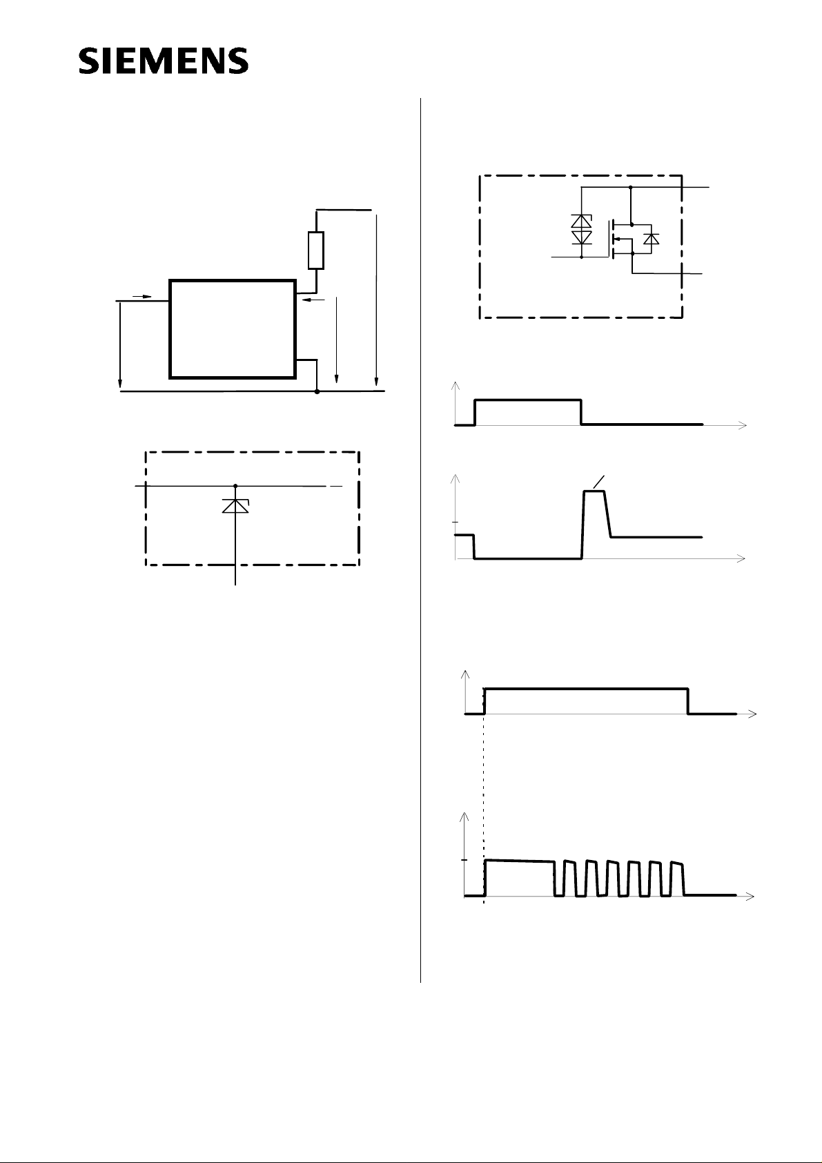
Block diagram
Terms
R
L
I
IN
V
IN
IN
1
HITFET
Input circuit (ESD protection)
IN
ESD-ZD
ESD zener diodes are not designed for DC
current.
I
Source
2
D
I
D
3
S
Inductive and overvoltage output clamp
V
Z
V
V
bb
DS
V
V
V
DS
V
DS(AZ)
D
S
HITFET
t
Turn on into overload or short circuit
V
IN
I
D
I
D(lim)
t
Shut down by overtemperature and restart by
cooling. Current internally limited at I
D(lim)
.
Semiconductor Group Page 5 1998-02-04
Page 6
HITFET® BSP 75
1000
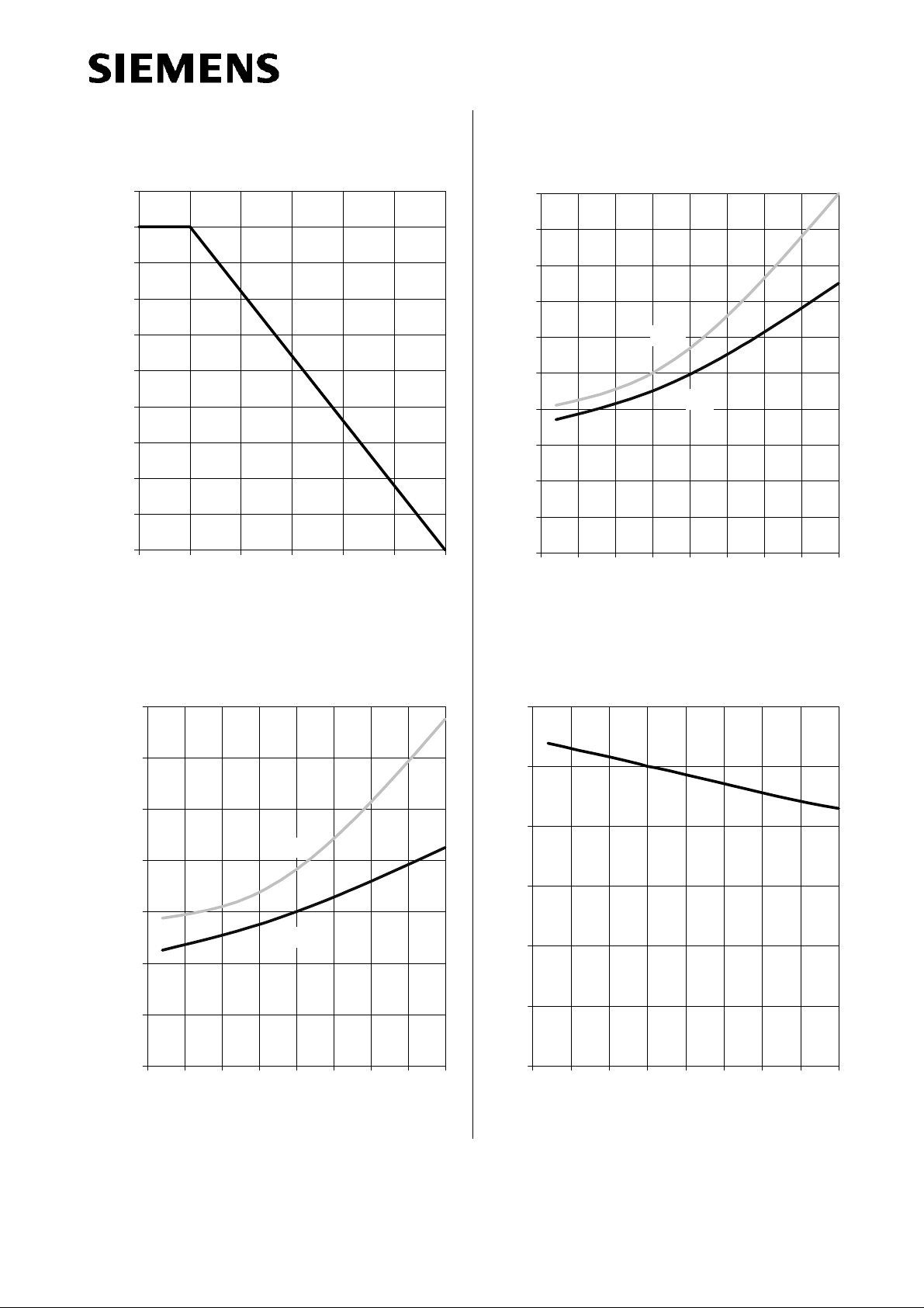
Maximum allowable power dissipation
= f (TC)
P
tot
P
[W]
tot
2
1.8
1.6
1.4
1.2
1
0.8
0.6
0.4
0.2
0
0 25 50 75 100 125 150
On-state resistance
= f (Tj); ID= 0.7 A; VIN= 10 V
R
ON
R
[mΩ]
ON
900
800
700
600
500
400
300
200
100
0
-50 -25 0 25 50 75 100 125 150
max.
typ .
On-state resistance
= f (Tj); ID= 0.7 A; VIN= 5 V
R
ON
R
[mΩ]
ON
1400
1200
1000
800
600
400
200
max.
typ .
TC [°C]
Typ. input threshold voltage
V
V
= f (Tj); ID= 10 mA; VDS= 12 V
IN(th)
[V]
IN(th)
3
2.5
2
1.5
1
0.5
Tj [°C]
0
-50 -25 0 25 50 75 100 125 150
Tj [°C]
0
-50 -25 0 25 50 75 100 125 150
Tj [°C]
Semiconductor Group Page 6 1998-02-04
Page 7
HITFET® BSP 75
1E+2
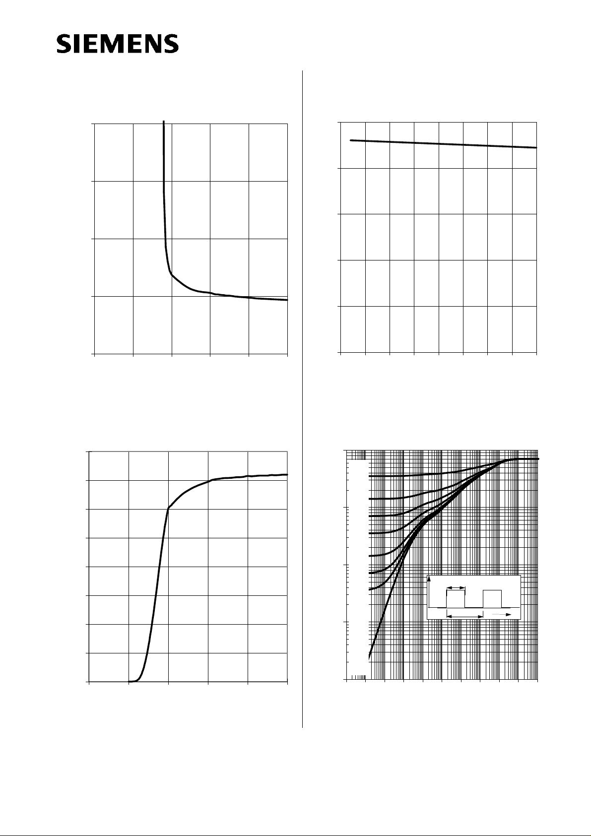
Typ. on-state resistance
= f (VIN) ID= 0.7 A; Tj= 25°C
R
ON
R
[mΩ]
ON
2000
1500
1000
500
0
0246810
Typ. current limitation
I
I
= f (Tj); VDS=12V, VIN= 10V
D(lim)
[A]
D(lim)
1.5
1.4
1.3
1.2
1.1
1
-50 -25 0 25 50 75 100 125 150
V
[V]
IN
Typ. short circuit current
= f (VIN); VDS=12V, Tj= 25°C
I
D(SC)
I
[A]
D(SC)
1.6
1.4
1.2
1
0.8
0.6
0.4
0.2
0
0246810
V
[V]
IN
Transient thermal impendance
= f (tp)
Z
thJC
Parameter: D=tp/T
Z
[K/W]
thJC
D=
0.5
0.2
1E+1
1E+0
0.1
0.05
0.01
0.02
0.005
P
tot
1E-1
0
1E-2
1E-6
1E-5
1E-4
1E-3
1E-2
1E-1
T
[°C]
j
t
p
T
1E+0
t
1E+1
1E+2
1E+3
1E+4
t
[s]
p
Semiconductor Group Page 7 1998-02-04
Page 8
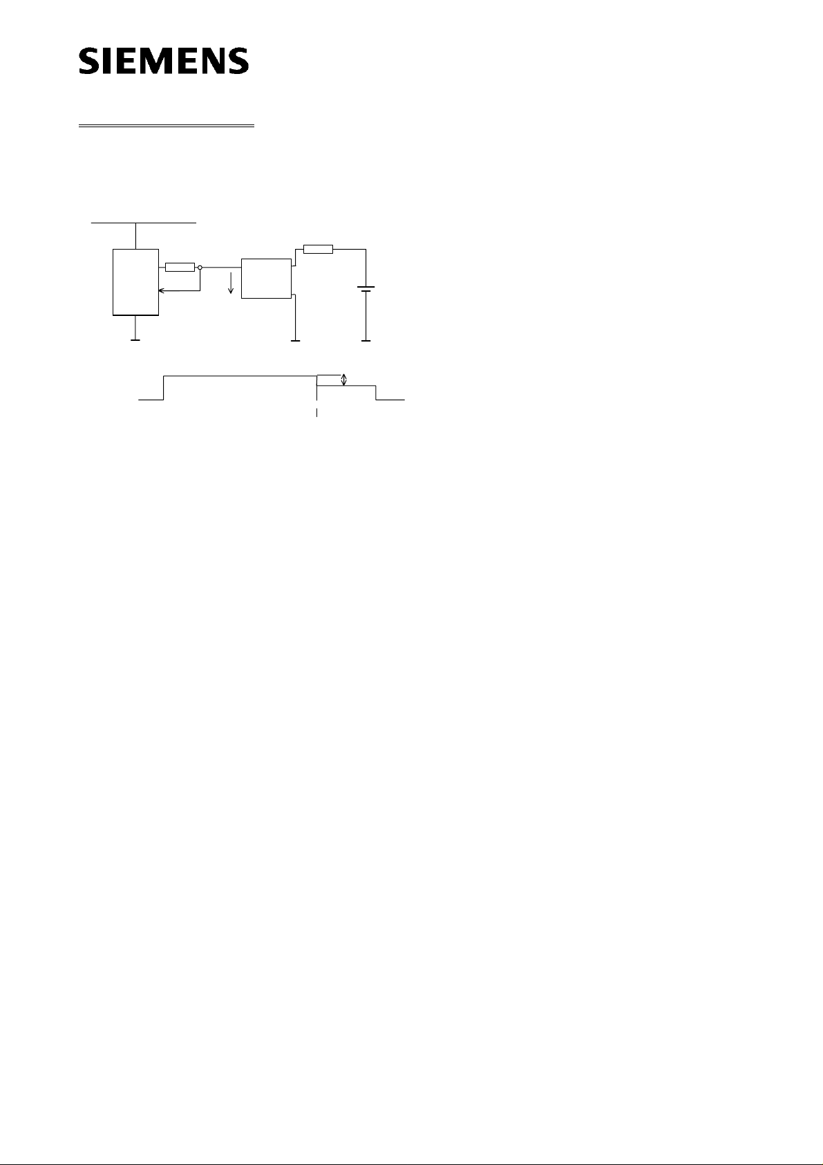
Application examples:
Status signal of thermal shutdown by monitoring
input current
R
St
µC
µC
V
IN
V
IN
IN
HITFET
D
S
thermal shutdown
V
bb
V
∆
HITFET® BSP 75
Semiconductor Group Page 8 1998-02-04
Page 9
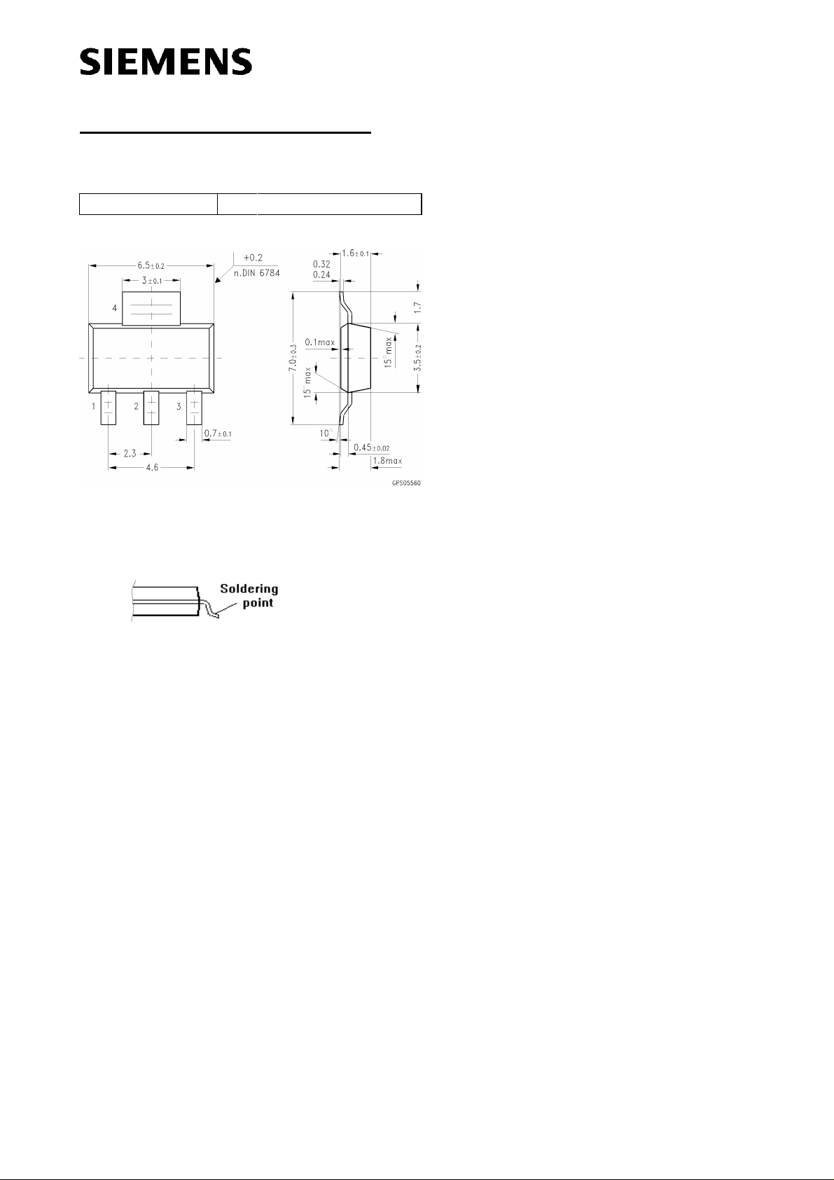
Package and ordering code
all dimensions in mm
SOT223/4 Ordering code
BSP75 Q67060-S7200-A2
HITFET® BSP 75
Definition of soldering point with temperature Ts:
upper side of solder edge of device pin 4.
Pin 4
Semiconductor Group Page 9 1998-02-04
 Loading...