

Page 1

DATA SH EET
Product specification
File under Discrete Semiconductors, SC07
1995 Apr 07
DISCRETE SEMICONDUCTORS
Philips Semiconductors
BSP304; BSP304A
P-channel enhancement mode
vertical D-MOS transistors
Page 2
1995 Apr 07 2
Philips Semiconductors Product specification
P-channel enhancement mode
vertical D-MOS transistors
BSP304; BSP304A
FEATURES
• Direct interface to C-MOS, TTL etc.
• High speed switching
• No secondary breakdown.
APPLICATIONS
• Intended for use as a Line current interruptor in
telephone sets and for applications in relay, high speed
and line transformer drivers.
DESCRIPTION
P-channel enhancement mode vertical D-MOS transistor
in a TO-92 variant package.
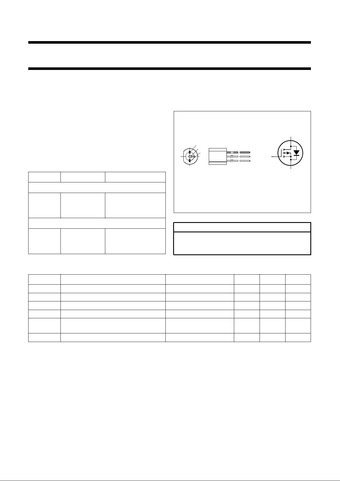
PINNING - TO-92 variant
PIN SYMBOL DESCRIPTION
BSP304
1 g gate
2 d drain
3 s source
BSP304A
1 s source
2 g gate
3 d drain
CAUTION
The device is supplied in an antistatic package. The
gate-source input must be protected against static
discharge during transport or handling.
Fig.1 Simplified outline and symbol.
handbook, halfpage
s
d
g
MAM144
1
3
2
QUICK REFERENCE DATA
SYMBOL PARAMETER CONDITIONS MIN. MAX. UNIT
V
DS
drain-source voltage (DC) −−300 V
V
GSO
gate-source voltage (DC) open drain −±20 V
V
GSth
gate-source threshold voltage ID= −1 mA; VDS=V
GS
−1.7 −2.55 V
I
D
drain current (DC) −−170 mA
R
DSon
drain-source on-state resistance ID= −170 mA;
VGS= −10 V
− 17 Ω
P
tot
total power dissipation up to T
amb
=25°C − 1W
Page 3

1995 Apr 07 3
Philips Semiconductors Product specification
P-channel enhancement mode
vertical D-MOS transistors
BSP304; BSP304A
LIMITING VALUES
In accordance with the Absolute Maximum Rating System (IEC 134).
THERMAL CHARACTERISTICS
Note to the “Limiting values” and “Thermal characteristics”
1. Device mounted on a printed-circuit board, maximum lead length 4 mm; mounting pad for drain lead minimum 1 cm
2
.
CHARACTERISTICS
T
j
=25°C unless otherwise specified.
SYMBOL PARAMETER CONDITIONS MIN. MAX. UNIT
V
DS
drain-source voltage (DC) −−300 V
V
GSO
gate-source voltage (DC) open drain −±20 V
I
D
drain current (DC) −−170 mA
I
DM
peak drain current −−0.75 A
P
tot
total power dissipation up to T
amb
=25°C; note 1 − 1W
T
stg
storage temperature −65 +150 °C
T
j
operating junction temperature − 150 °C
SYMBOL PARAMETER CONDITIONS VALUE UNIT
R
th j-a
thermal resistance from junction to ambient note 1 125 K/W
SYMBOL PARAMETER CONDITIONS MIN. TYP. MAX. UNIT
V
(BR)DSS
drain-source breakdown voltage VGS= 0; ID= −10 µA −300 −−V
V
GSth
gate-source threshold voltage VDS=VGS; ID= −1mA −1.7 −−2.55 V
I
DSS
drain-source leakage current VGS= 0; VDS= −240 V −−−100 nA
I
GSS
gate leakage current VGS= ±20 V; VDS=0 −−±100 nA
R
DSon
drain-source on-state resistance VGS= −10 V; ID= −170 mA −−17 Ω
y
fs
forward transfer admittance VDS= −25 V; ID= −170 mA 100 −−mS
C
iss
input capacitance VGS= 0; VDS= −25 V; f = 1 MHz − 60 90 pF
C
oss
output capacitance VGS= 0; VDS= −25 V; f = 1 MHz − 15 30 pF
C
rss
reverse transfer capacitance VGS= 0; VDS= −20 V; f = 1 MHz − 515pF
Switching times (see Figs 2 and 3)
t
on
turn-on time VGS=0to−10 V; VDD= −50 V;
ID= −250 mA
− 510ns
t
off
turn-off time VGS= −10 to 0 V; VDD= −50 V;
ID= −250 mA
− 15 30 ns
Page 4

1995 Apr 07 4
Philips Semiconductors Product specification
P-channel enhancement mode
vertical D-MOS transistors
BSP304; BSP304A
Fig.2 Switching time test circuit.
handbook, halfpage
MBB689
50 Ω
I
D
10 V
0
V = 50 V
DD
Fig.3 Input and output waveforms.
handbook, halfpage
MBB690
10 %
90 %
90 %
10 %
t
on
t
off
OUTPUT
INPUT
Fig.4 Power derating curve.
handbook, halfpage
0 200
0
0.4
0.8
1.2
MLC697
T ( C)
amb
o
50 100 150
P
tot
(W)
δ = 0.01.
T
amb
=25°C.
(1) R
DSon
limitation.
Fig.5 DC SOAR.
handbook, halfpage
MLC699
11010
V
DS
(V)
I
D
(A)
1
2
1
10
2
10
t
p
T
P
t
t
p
T
δ
=
1 s
100 µs
1 ms
10 ms
100 ms
DC
(1)
tp =
10 µs
3
10
10
3
Page 5

1995 Apr 07 5
Philips Semiconductors Product specification
P-channel enhancement mode
vertical D-MOS transistors
BSP304; BSP304A
Fig.6 Capacitance as a function of drain source
voltage; typical values.
VGS=0.
Tj=25°C.
f = 1 MHz.
handbook, halfpage
0
100
60
80
40
20
0
10 20 30
MLC688
C
(pF)
V (V)
DS
C
oss
C
rss
C
iss
Fig.7 Typical output characteristics.
Tj=25°C.
handbook, halfpage
024 10
800
600
200
0
400
MLD139
6
I
D
(mA)
V (V)
DS
128
P = 1 W
V = 10 V
GS
7 V
6 V
5 V
4 V
3.5 V
3 V
Fig.8 Typical transfer characteristics.
VDS= −25 V.
Tj=25°C.
handbook, halfpage
024 10
800
600
200
0
400
MLC689
6
I
D
(mA)
V (V)
GS
8
Fig.9 Drain-source on-state resistance as a function
of gate-source voltage; typical values.
ID= −170 mA.
Tj=25°C.
handbook, halfpage
0
20
40
60
80
0246810
R
DSon
(Ω)
V (V)
GS
MLC691
Page 6

1995 Apr 07 6
Philips Semiconductors Product specification
P-channel enhancement mode
vertical D-MOS transistors
BSP304; BSP304A
Fig.10 Drain-source on-state resistance as a
function of drain current; typical values.
Tj=25°C.
handbook, halfpage
0
10
20
30
40
50
60
1 101010
I
D
(mA)
VGS= 3 V
4 V 5 V
7 V
10 V
MLC692
23
6 V
R
DSon
(Ω)
Fig.11 Temperature coefficient of gate-source
threshold voltage.
Typical V
GSth
at ID= −1 mA; VDS=VGS.
k
V
GSth
at T
j
V
GSth
at 25°C
--------------------------------------
=
handbook, halfpage
0.8
0.9
1.0
1.1
0 50 100 15050
k
T ( C)
j
o
MLC696
Fig.12 Temperature coefficient of drain-source
on-state resistance.
Typical R
DSon
at ID= −170 mA; VGS= −10 V.
k
R
DSon
at T
j
R
DSon
at 25 °C
-----------------------------------------
=
handbook, halfpage
0
0.5
1
1.5
2
2.5
0 50 100 150
k
T ( C)
j
o
MLC695
50
Page 7

1995 Apr 07 7
Philips Semiconductors Product specification
P-channel enhancement mode
vertical D-MOS transistors
BSP304; BSP304A
Fig.13 Transient thermal resistance from junction to ambient as a function of pulse time; typical values.
T
amb
=25°C.
handbook, full pagewidth
1
10
0.5
0.2
0.1
0.05
0.02
0.01
0
110
10
3
10
2
10
3
(K/W)
MLC698
tp (s)
0.75
δ
=
10
2
t
p
T
P
t
t
p
T
δ
=
R
th j-a
1
10
5
10
2
10
1
10
3
10
4
10
Page 8

1995 Apr 07 8
Philips Semiconductors Product specification
P-channel enhancement mode
vertical D-MOS transistors
BSP304; BSP304A
PACKAGE OUTLINE
Fig.14 TO-92 variant.
Dimensions in mm.
(1) Terminal dimensions within this zone are uncontrolled to allow for flow of plastic and terminal irregularities.
handbook, full pagewidth
MBC015 - 1
2.54
4.8
max
4.2 max
1.6
0.66
0.56
1
2
3
5.2 max 12.7 min
2.5 max
(1)
0.48
0.40
0.40
min
Page 9

1995 Apr 07 9
Philips Semiconductors Product specification
P-channel enhancement mode
vertical D-MOS transistors
BSP304; BSP304A
DEFINITIONS
LIFE SUPPORT APPLICATIONS
These products are not designed for use in life support appliances, devices, or systems where malfunction of these
products can reasonably be expected to result in personal injury. Philips customers using or selling these products for
use in such applications do so at their own risk and agree to fully indemnify Philips for any damages resulting from such
improper use or sale.
Data Sheet Status
Objective specification This data sheet contains target or goal specifications for product development.
Preliminary specification This data sheet contains preliminary data; supplementary data may be published later.
Product specification This data sheet contains final product specifications.
Limiting values
Limiting values given are in accordance with the Absolute Maximum Rating System (IEC 134). Stress above one or
more of the limiting values may cause permanent damage to the device. These are stress ratings only and operation
of the device at these or at any other conditions above those given in the Characteristics sections of the specification
is not implied. Exposure to limiting values for extended periods may affect device reliability.
Application information
Where application information is given, it is advisory and does not form part of the specification.
 Loading...