

Page 1
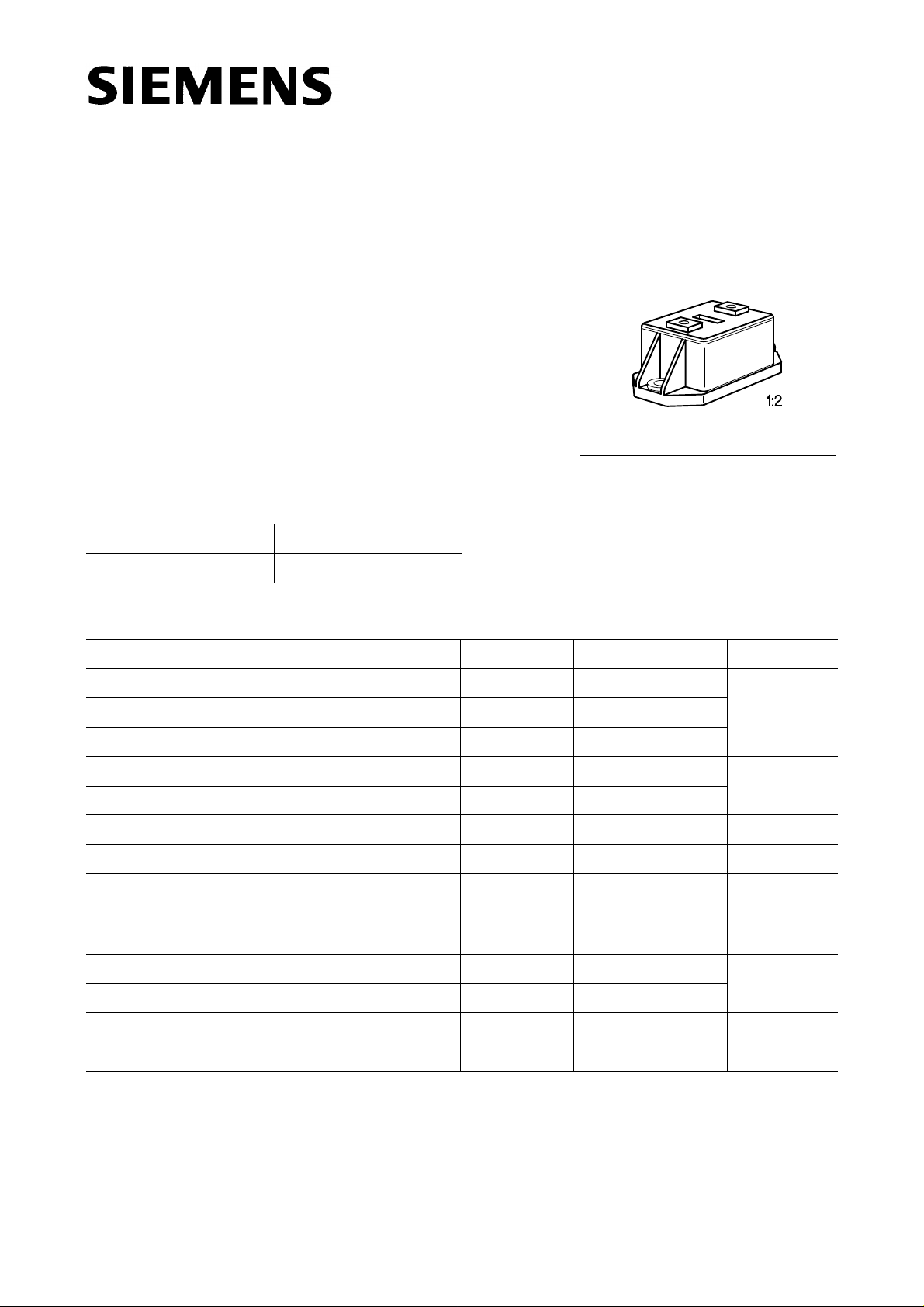
SIMOPAC® Module BSM 151 F
V
I
R
● Power module
● Single switch
● FREDFET
● N channel
● Enhancement mode
● Package with insulated metal base plate
● Package outline/Circuit diagram: 1
DS
D
DS(on)
= 500 V
= 56 A
= 0.11 Ω
1)
Type Ordering Code
BSM 151 F C67076-A1050-A2
Maximum Ratings
Parameter Symbol Values Unit
Drain-source voltage
Drain-gate voltage,
R
= 20 kΩ V
GS
Gate-source voltage
Continuous drain current,
Pulsed drain current,
T
= 32 ˚C I
C
T
= 32 ˚C I
C
Operating and storage temperature range
Power dissipation,
T
= 25 ˚C P
C
Thermal resistance
Chip-case
2)
Insulation test voltage
, t = 1 min. V
V
V
D
D puls
T
j
R
DS
DGR
GS
, T
tot
th JC
is
stg
500 V
500
± 20
56 A
224
– 55 … + 150 ˚C
700 W
K/W
≤ 0.18
2500 V
ac
Creepage distance, drain-source – 16 mm
Clearance, drain-source – 11
DIN humidity category, DIN 40 040 – F –
IEC climatic category, DIN IEC 68-1 – 55/150/56
1)
See chapter Package Outline and Circuit Diagrams.
2)
Insulation test voltage between drain and base plate referred to standard climate 23/50 in acc. with
DIN 50 014, IEC 146, para. 492.1.
Semiconductor Group 50 03.96
Page 2
BSM 151 F
Electrical Characteristics
at Tj = 25 ˚C, unless otherwise specified.
Parameter Symbol Values Unit
min. typ. max.
Static Characteristics
Drain-source breakdown voltage
V
= 0, ID = 0.25 mA
GS
Gate threshold voltage
V
= VGS, ID = 1 mA
DS
Zero gate voltage drain current
V
= 500 V, VGS = 0
DS
T
= 25 ˚C
j
T
= 125 ˚C
j
Gate-source leakage current
V
= 20 V, VDS = 0
GS
Drain-source on-state resistance
V
= 10 V, ID = 36 A
GS
Dynamic Characteristics
Forward transconductance
V
≥ 2 × ID× R
DS
DS(on)max.
, ID = 36 A
Input capacitance
V
= 0, VDS = 25 V, f = 1 MHz
GS
Output capacitance
V
= 0, VDS = 25 V, f = 1 MHz
GS
Reverse transfer capacitance
V
= 0, VDS = 25 V, f = 1 MHz
GS
t
Turn-on time
V
= 250 V, VGS = 10 V
CC
I
= 36 A, RGS = 3.3 Ω
D
Turn-off time
V
= 250 V, VGS = 10 V
CC
I
= 36 A, RGS = 3.3 Ω
D
(ton = t
on
t
off(toff
= t
d (on)
d (off)
+ tr)
+ tf)
V
(BR)DSS
V
GS(th)
I
DSS
I
GSS
R
DS(on)
g
fs
C
iiss
C
oss
C
rss
t
d (on)
t
r
t
d (off)
t
f
V
500 – –
2.1 3.0 4.0
µA
–
–
50
300
250
1000
nA
– 10 100
Ω
– 0.09 0.11
20 30 – S
–2230nF
– 1.6 2.4
– 0.65 1.0
–60–ns
–35–
– 350 –
–70–
Semiconductor Group 51
Page 3

BSM 151 F
Electrical Characteristics (cont’d)
at Tj = 25 ˚C, unless otherwise specified.
Parameter Symbol Values Unit
min. typ. max.
Fast-recovery reverse diode
Continuous reverse drain current
T
= 25 ˚C
C
Pulsed reverse drain current
T
= 25 ˚C
C
Diode forward on-voltage
I
= 96 A , VGS = 0
F
Reverse recovery time
I
= IS, diF/dt = 100 A/ µs, VR = 100 V
F
T
= 25 ˚C
j
T
= 150 ˚C
j
Reverse recovery charge
I
= IS, diF/dt = 100 A/ µs, VR = 100 V
F
T
= 25 ˚C
j
T
= 150 ˚C
j
Repetitive peak reverse current
I
= IS, diF/dt = 100 A/ µs, VR = 100 V
F
T
= 25 ˚C
j
T
= 150 ˚C
j
I
I
V
t
Q
I
rr
S
SM
SD
rr
RRM
––56
– – 224
– 1.3 1.6
–
–
–
–
–
–
200
350
1.5
8.5
12
28
280
500
2.5
12
–
–
A
V
ns
µC
A
Semiconductor Group 52
Page 4

Characteristics at
Power dissipation
T
P
parameter: Tj = 150 ˚C
= 25 ˚C, unless otherwise specified.
j
= f (TC)
tot
Typ. output characteristics ID = f (VDS)
parameter: tp = 80 µs pulse test
BSM 151 F
Safe operating area ID = f (VDS)
parameter: single pulse, TC = 25 ˚C,
T
≤ 150 ˚C (VDS)
j
Typ. transfer characteristic ID = f (VGS)
parameter: tp = 80 µs , VDS = 25 V
Semiconductor Group 53
Page 5

BSM 151 F
Continuous drain current
I
= f (TC)
D
parameter: VGS ≥ 10 V, T j = 150 ˚C
Drain-source breakdown voltage
V
(BR)DSS
(Tj) = b × V
(BR)DSS
(25 ˚ C)
Drain source on-state resistance
R
= f (Tj)
DS(on)
parameter: ID= 36 A; VGS = 10 V, (spread)
Typical capacitances C = f (VDS)
parameter: VGS = 0, f =1 MHz
Semiconductor Group 54
Page 6

BSM 151 F
Forward characteristics of fast-recovery
reverse diode IF = f (VSD)
parameter: Tj, tp = 80 µs (spread)
Typ. reverse recovery Qrr = f (Tj)
parameter:di/dt = 100 A/ µs, IF = 56 A
V
= 100 V
R
Semiconductor Group 55
Page 7

BSM 151 F
Transient thermal impedance Z
parameter: D = t
/T
p
thJC
= f (tp)
Typ. gate charge VGS = f (Q
parameter: I
Dpuls
= 75 A
Gate
)
Semiconductor Group 56
 Loading...