

Page 1
1
Memory ICs
1,024-Bit Serial Electrically Erasable PROM
BR93LL46F / BR93LL46FV
•
Features
• Low power CMOS technology
• 64 × 16 bit configuration
• 1.8V to 4.0V operation
• Low power dissipation
– 0.5mA (typ.) active current
– 0.4µA (typ.) standby current
• Auto increment for efficient data dump
• Automatic erase-before-write
• Hardware and software write protection
– Defaults to write-disabled state at power up
– Software instructions for write-enable / disable
– Vcc lockout inadvertent write protection
• 8-pin SOP / 8-pin SSOP-B packages
• Device status signal during write cycle
• 100,000 ERASE / WRITE cycles
• 10 years Data Retention
•
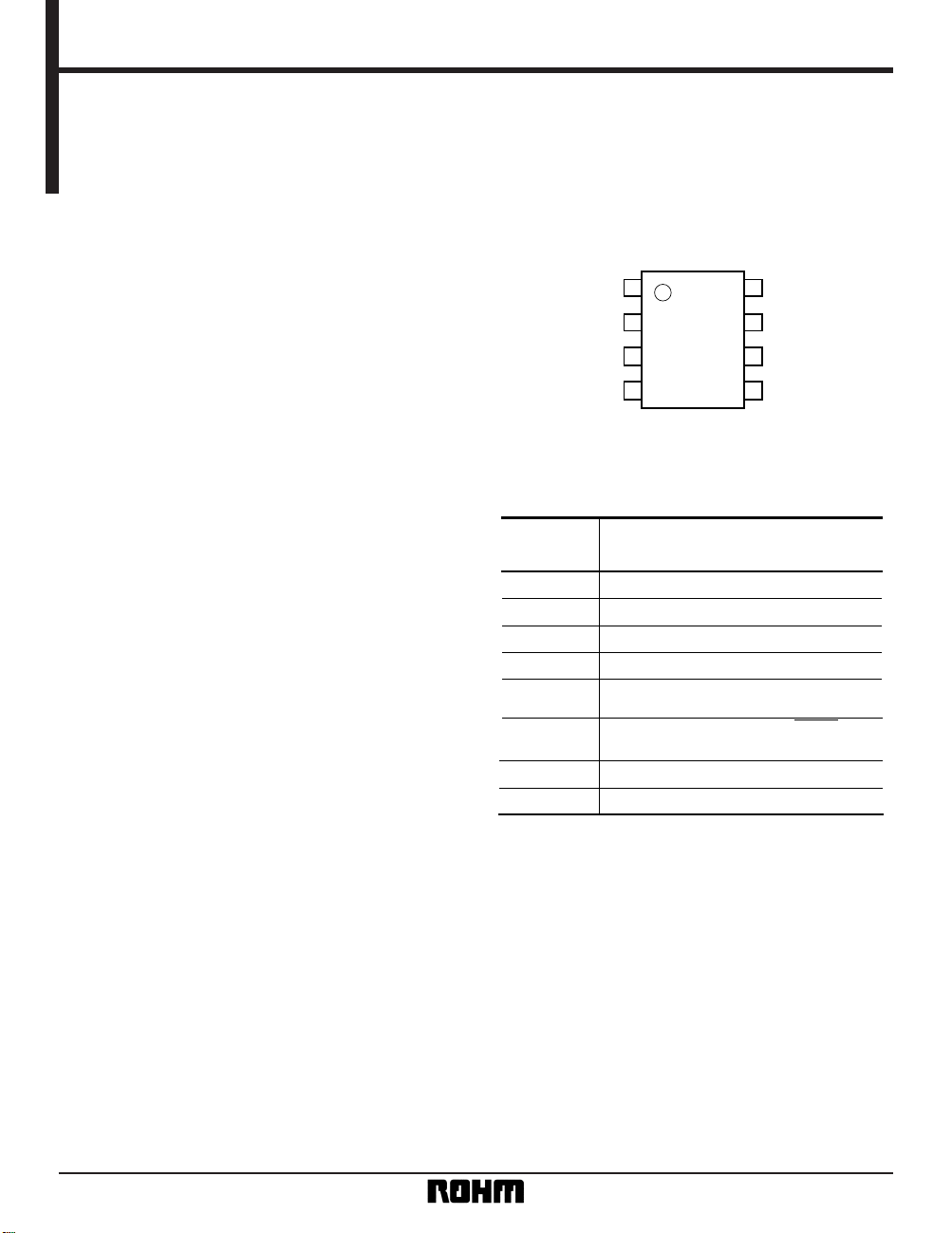
Pin assignments
•
Pin descriptions
1
2
3
4
5
6
7
8
DO
DISK
N.C. N.C.
CS
GND
BR93LL46F
BR93LL46FV
VCC
(SOP8 / SSOP-B8)
Pin Name Function
N.C. Not connected
Power supply
Chip select input
Serial clock input
Start bit, operating code, address, and
serial data input
Serial data output, READY / BUSY
internal status display output
Ground
Not connected
V
CC
CS
SK
DI
DO
GND
N.C.
•
Overview
The BR93LC46F and BR93LL46FV are CMOS serial input / output-type memory circuits (EEPROMs) that can be
programmed electrically. Each is configured of 64 words × 16 bits (1,024 bits), and each word can be accessed indi-
vidually and data read from it and written to it. Operation control is performed using five types of commands. The
commands, addresses, and data are input through the DI pin under the control of the CS and SK pins. In a write
operation, the internal status signal (READY or BUSY) can be output from the DO pin.
Page 2
2
Memory ICs BR93LL46F / BR93LL46FV
•
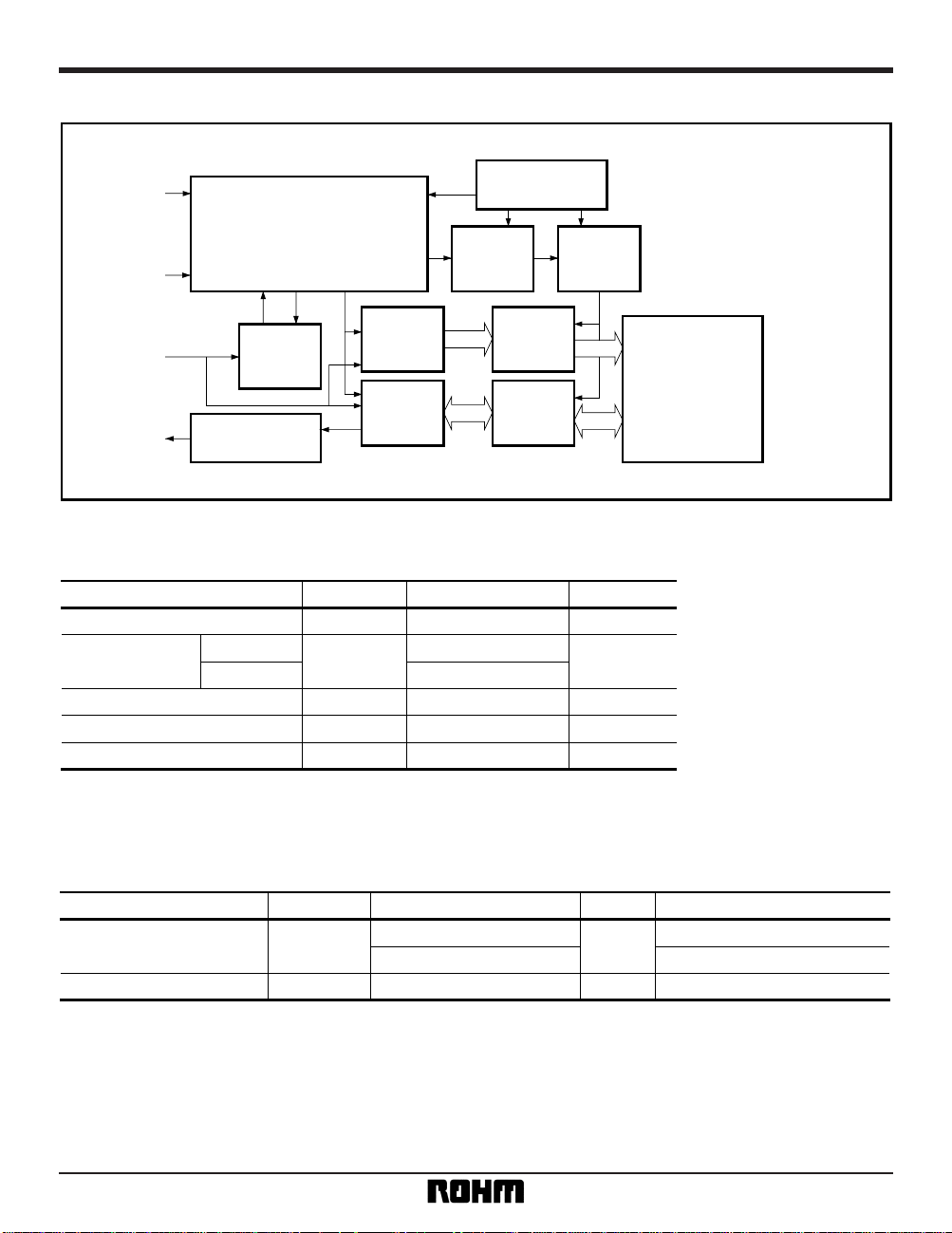
Block diagram
Command
register
Data
register
Address
buffer
Dummy bit
DO
DI
SK
CS
16bit
16bit
6bit
6bit
Address
decoder
Command decode
Control
Clock generation
Power supply
voltage detector
High voltage
generator
Write
disable
1,024-bit
EEPROM array
R / W
AMP.
•
Absolute maximum ratings
Parameter Symbol Limits Unit
V
CC – 0.3 ~ + 7.0 V
Pd
350
∗
1
300
∗
2
BR93LL46F
BR93LL46FV
mW
Tstg – 65 ~ + 125 °C
Topr – 20 ~ + 70 °C
— – 0.3 ~ V
CC + 0.3 V
∗
1 Reduced by 3.5mW for each increase in Ta of 1°C over 25°C.
∗
2 Reduced by 3.0mW for each increase in Ta of 1°C over 25°C.
Applied voltage
Power dissipation
Storage temperature
Operating temperature
Terminal voltage
•
Recommended operating conditions
Parameter Symbol Limits Unit Conditions
Power supply voltage
Input voltage
V
CC
1.8 ~ 4.0
2.0 ~ 4.0
Ta = 0 ~ 70°C
Ta = – 20 ~ + 70°C
V
0 ~ V
CC VV
IN —
Page 3
3
Memory ICs BR93LL46F / BR93LL46FV
•
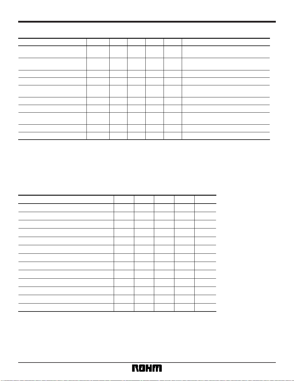
Electrical characteristics (unless otherwise noted, Ta = – 20 to + 70°C, VCC = 1.8 to 4.0V)
Parameter Symbol Min. Typ. Max. Unit Conditions
V
IL – 0.3 —
0.2
V
× V
CC
VIH
0.8
—
VCC +
V
0.3× V
CC
VOL1 — — 0.3 V IOL = 1.0mA
V
OL2 — — 0.2 V IOL = 20µA
V
OH2
VCC –
——VI
OH = 100µA
0.3
I
LI – 1.0 — µAVIN = 0V ~ VCC
ILO – 1.0 — µAVOUT = 0V ~ VCC, CS = GND
I
CC1 — 0.5 1.0 mA
V
IN = VIH / VIL, DO = OPEN, fSK = 250kHz
WRITE
I
CC2 — 0.4 1.0 mA
VIN = VIH / VIL, DO = OPEN, fSK = 250kHz, READ
ISB — 0.4 1.0 µA CS = SK = DI = GND, DO = OPEN
1.0
1.0
∗
1 About the operating current dissipation
I
CC1
indicates the average current dissipation during a writing operation, and I
CC2
indicates the average current dissipation during a reading operation.
Because this is internal logic switching current, it changes based on the SK frequency.
∗
2 About the standby current
This is the current dissipation when all inputs are CMOS level and in static state.
Input low level voltage
Input high level voltage
Output low level voltage 1
Output low level voltage 2
Output high level voltage 2
Input leakage current
Output leakage current
Operating current dissipation 1
Operating current dissipation 2
Standby current
—
—
•
Operation timing characteristics (Ta = – 20 to + 70°C, VCC = 1.8 to 4.0 V)
Parameter Symbol Min. Typ. Max. Unit
SK clock frequency
SK "H" time
SK "L" time
CS "L" time
CS setup time
DI setup time
CS hold time
DI hold time
Data "1" output delay time
Data "0" output delay time
Time from CS to output confirmation
Time from CS to output High impedance
Write cycle time
f
SK — — 250 kHz
t
SKH 1——µs
t
SKL 1——µs
t
CS 1——µs
t
CSS 200 — — ns
t
DIS 400 — — ns
t
CSH 0——ns
t
DIH 400 — — ns
t
PD1 ——2 µs
t
PD0 ——2 µs
t
SV —— 2 µs
t
DF — — 400 ns
t
E / W ——25ms
Page 4
4
Memory ICs BR93LL46F / BR93LL46FV
•
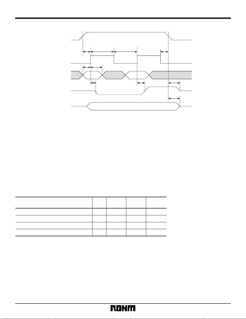
Timing chart
CS
SK
DI
STATUS VALID
DO (READ)
DO (WRITE)
tDIS
tSKH tSKL
tCSH
tDIH
tDF
tDF
tCSS
tPD0
tPD1
Fig. 1 Synchronous data timing
(1) Data is acquired from DI in synchronization with the
SK rise.
(2) During a reading operation, data is output from DO
in synchronization with the SK rise.
(3) During a writing operation, a Status Valid (READY
or BUSY) is valid from the time CS is HIGH until time
t
CS after CS falls following the input of a write command
and before the output of the next command start bit.
Also, DO must be in a HIGH-Z state when CS is LOW.
(4) After the completion of each mode, make sure that
CS is set to LOW, to reset the internal circuit, before
changing modes.
•
Circuit operation
(1) Command mode
Command
Start
bit
Operating
code
Address Data
1 10 A5 ~ A0
1 00 11XXXX
1 01 A5 ~ A0 D15 ~ D0
1 00 00XXXX
X: Either VIH or VIL
Read (READ)
Write enabled (WEN)
Write (WRITE)
Write disabled (WDS)
(
∗
1
)
W
(
∗
2
)
—
—
—
∗ About the start bit
With these ICs, commands are not recognized or acted
upon until the start bit is received. The start bit is taken
as the first “1” that is received after the CS pin rises.
(∗1) After setting of the read command and input of the
SK clock, data corresponding to the specified address
is output, with data corresponding to upper addresses
then output in sequence. (Auto increment function)
(∗2) When the write command is executed, all data in
the selected memory cell is erased automatically, and
the input data is written to the cell.
Page 5

5
Memory ICs BR93LL46F / BR93LL46FV
(2) Reading
A0A1
11
0 D15 D14 D0D1
0
A5 A4
D14D15
1 2 4 9 10 25 26
CS
SK
DI
DO
(
∗
1
)
(
∗
2
)
High-Z
Fig.2 Read cycle timing (READ)
100 11
CS
SK
DI
DO
High-Z
Fig.3 Cycle timing that allows overwriting
When the read command is acknowledged, the data
(16 bits) for the input address is output serially. The
data is synchronized with the SK rise during A0 acquisition and a “0” (dummy bit) is output. All further data is
output in synchronization with the SK pulse rises.
( ∗1) Start bit
The start bit is taken as the first “1” that is received
after the CS pin rises. Also, if “0” is input several times
followed by “1”, the “1” is recognized as a start bit, and
subsequent operation commences.
This applies also to the following commands.
( ∗2) Address auto increment function
These ICs are equipped with an address auto increment function which is effective only during reading
operations. With this function, if the SK clock is input
following execution of one of the above reading commands, data is read from upper addresses in succession. CS is held in HIGH state during automatic incrementing.
(3) Write enable These ICs are set to the write disabled state by the
internal reset circuit when the power is turned on.
Therefore, before performing a write command, the
write enable command must be executed. When this
command is executed, it remains valid until a write disable command is issued or the power supply is cut off.
However, read commands can be used in either the
write enable or write disable state.
Page 6

6
Memory ICs BR93LL46F / BR93LL46FV
(4) Write
A0A110 D15 D14 D0D1
READYBUSY
STATUS
1A5A4
12 4 910
25
CS
SK
DI
DO
High-Z
t
CS
tSV
tE / W
Fig. 4 Write cycle timing (WRITE)
100 00
CS
SK
DI
DO
High-Z
Fig. 5 Write disable cycle timing (WDS)
This command writes the 16-bit data (D15 to D0) to the
specified address (A5 to A0). The actual writing begins
when CS falls following the fall of the SK cloc (the 25th
clock pulse after the start bit) when D0 is read.
If STATUS is not detected (CS is fixed at LOW, or if
STATUS is detected (CS is HIGH) at timing t
E / W, no
commands will be received as long as a LOW state
(BUSY) is output from DO, so command input should
be avoided.
∗ STATUS
After time t
CS following the fall of CS, after input of the
write command, if CS is set to HIGH, the write execute
= BUSY (LOW) and the command wait status READY
(HIGH) are output.
If in the command wait status (STATUS = READY), the
next command can be performed within the time t
E / W
Thus, if data is input via SK and DI with CS = HIGH in
the t
E / W period, erroneous operations may be per-
formed. To avoid this, make sure that DI = LOW when
CS = HIGH. (Caution is especially important when
common input ports are used.) This applies to all of the
write commands.
(5) Write disable When the power supply is turned on, if the write enable
command is issued, the write enable state is entered. If
the write disable command is then issued, the IC
enters the write disable status. When in this status, all
write commands are ignored, but read commands may
be executed.
In the write enable status, writing begins even if a write
command is entered accidentally. To prevent errors of
this type, we recommend executing a write disable
command after writing has been completed.
Page 7

7
Memory ICs BR93LL46F / BR93LL46FV
2bits
6bits
〈READ〉
1bit 16bits
a
6bits
2bits
1bit
16bits
b
〈WRITE〉
Start bit Operating code Address Data
Cancel can be performed for the entire read mode space
Cancellation method: CS LOW
Start bit Operating code Address Data tE / W
•
Operation notes
(1) Cancelling modes
Point a: Start bit position when error occurs
Point b: Actual start bit position
10
a
b
SK
CS
DI
10
b
SK
CS
DI
(Figure a. Erroneous operation timing) (Figure b. Normal operation timing)
a: Canceled by setting CS LOW or VCC OFF (夽)
b: Cannot be canceled by any method. If V
CC is set to
OFF during this time, the data in the designated
address is not secured.
夽: V
CC OFF (VCC is turned off after CS is set to LOW)
(2) Timing in the standby mode
As shown in Figure a, during standby, if CS rises when
SK is HIGH, the DI state may be read on the rising
edge. If this happens, and DI is HIGH, this is taken to
be the start bit, causing a bit error (see point “a” in
Figure a).
Make sure all inputs are LOW during standby or when
turning the power supply on or off (see Figure b).
Page 8

8
Memory ICs BR93LL46F / BR93LL46FV
CS
GND
GND
Bad example
Good example
+ 5V
+ 5V
V
CC
Fig.6
(3) Precautions when turning power on and off
䊊When turning the power supply on and off, make
sure CS is set to LOW (see Figure 6).
When CS is HIGH, the EEPROM enters the active
state. If the power supply is turned on in this state,
noise and other factors can cause malfunctions and
erroneous writing. To avoid this, make sure CS is set to
LOW (disable mode) when turning on the power supply. (When CS is LOW, all input is cancelled.)
When the power supply is turned off, the low power
state can continue for a long time because of the
capacity of the power supply line. Erroneous operations and erroneous writing can occur at such times for
the same reasons as described above. To avoid this,
make sure CS is set to LOW before turning off the
power supply.
To prevent erroneous writing, these ICs are equipped
with a POR (Power On Reset) circuit, but in order to
achieve operation at a low power supply, V
CC is set to
operate at approximately 1.3V. After the POR has been
activated, writing is disabled, but if CS is set to HIGH,
writing may be enabled because of noise or other factors. However, the POR circuit is effective only when
the power supply is on, and will not operate when the
power is off. Also, to prevent erroneous writing at low
voltages, these ICs are equipped with a built-in circuit
which resets the write command if V
CC drops to approx-
imately 1.5V or lower (typ.)
(V
CC-lockout circuit)
(Bad example) Here, the CS pin is pulled up to V
CC.
In this case, CS is HIGH (active state).
Please be aware that the EEPROM
may perform erroneous operations or
write erroneous data because of noise
or other factors.
∗ Even if the CS input is HIGH-Z,
please be aware that cases such as
this can occur.
(Good example) In this case, CS is LOW when the
power supply is turned on or off.
(4) Clock (SK) rise conditions
If the clock pin (SK) signal of the BR93LL46F / FV has
a long rise time (Tr) and if noise on the signal line
exceeds a certain level, erroneous operation can occur
due to erroneous counts in the clock. To prevent this, a
Schmitt trigger is built into the SK input of the BR93LL46F / FV. The hysteresis amplitude of this circuit is
set to approximately 0.2V, so if the noise exceeds the
SK input, the noise amplitude should be set to 0.2 V
P-P
or lower. Furthermore, rises and falls in the clock input
should be accelerated as much as possible.
Page 9

9
Memory ICs BR93LL46F / BR93LL46FV
•
Operation notes
(5) Connecting DI and DO directly
The BR93LL46F / FV have an independent input pin
(DI) and output pin (DO). These are treated as individual signals on the timing chart but can be controlled
through one control line. Control can be initiated on a
single control line by treating these signals as separate
in the timing chart.
1) Data collision between the µ-COM output and the
DO output
Within the input and output timing of the BR93LL46F /
FV, the drive from the µ-COM output to the DI input
and a signal output from the DO output can be emitted
at the same time. This happens only for the 1 clock
cycle (a dummy bit “0” is output to the DO pin) which
acquires the A0 address data during a read cycle.
→ When the address data A0 = 1, a feedthrough current path occurs.
Timing after a write command, when CS is HIGH
A READY or BUSY function is output on the DO pin.
When the next start bit is input, DO goes to the high
impedance state.
→ When inputting a command after a write, when the
CS input rises while the µ-COM output remains LOW,
a READY output HIGH is output from the DO pin and
feedthrough current paths can occur.
2) When the µ-COM port is the CMOS port
The µ-COM port can be controlled by the 1 control line
by connecting a resistor R between the DI and DO pins
during CMOS input and output, as shown in Figure 7.
In this case, the value of R needs to satisfy the positive
portion of the µ-COM input level for the voltage drop at
R resulting from the leak current of the µ-COM input
and the DI pin. It must be as small as possible so that it
does not influence the DO output noise but large
enough to keep the feedthrough current to a minimum.
A value in the range of 1K-200kΩ is usually sufficient.
Make sure to confirm this through experiment. In this
case, a dummy bit cannot be detected.
3) Feedback to the DI input from the DO output
Data is output from the DO pin and then feeds back
into the DI input through the resistor R. This happens
when:
1. DO data is output during a read operation
2. A READY / BUSY signal is output during a write
operation
Such feedback does not cause problems in the basic
operation of the BR93LL46F / FV.
R
DI
DO
EEPROM
µ-COM
Fig. 7 Using the CMOS port
Page 10

10
Memory ICs BR93LL46F / BR93LL46FV
CS
SK
DI
DO
D1
D0
READY
BUSY
Write command Status detection
Command input
DI
DO
D1
D0
BUSY
READY
High-Z
High-Z
∗
DI: EEPROM DI terminal; DO: EEPROM DO output; DI / DO: µ-COM I / O terminal
Fig. 9 Timing diagram chart
4) When the µ-COM port is the open drain port
When the µ-COM port is the open drain output port, it
responds through software as shown in Figure 8. This
method will not work during CMOS input and output.
The timing which becomes a problem (production of
feedthrough current paths) for the open drain port only
occurs when CS is HIGH after a write command. Feedthrough current paths can occur in the period between
the rise of the CS to the input of the start bit. If CS rises
before the start bit, as shown in Figure 8, and DI is
HIGH at the same time, current paths are not created.
Make sure to set SK to LOW during a CS rise.
In this case, however, the first SK rise after the CS
rises is interpreted as the start bit. Therefore, caution is
required. Figure 9 shows a timing chart from the end of
a write command to the next command input. As
shown in the figure, after completion of the write command input, when CS rises, set SK to LOW and stop
the SK input. Otherwise, if DO is HIGH when a clock
pulse is input, this is taken as the start bit and may
cause erroneous operation.
Start bit
1
2
34
CS
SK
DI
DO
High-Z
Fig. 8 Using an open drain port
Page 11

11
Memory ICs BR93LL46F / BR93LL46FV
•
External dimensions (Units: mm)
SOP8 SSOP-B8
BR93LL46F BR93LL46FV
0.4 ± 0.11.27
0.15
0.3Min.
0.15 ± 0.1
0.11
6.2 ± 0.3
4.4 ± 0.2
5.0 ± 0.2
85
41
1.5 ± 0.1
0.1
0.22 ± 0.1
0.65
0.3Min.
548
1
6.4 ± 0.3
4.4 ± 0.2
3.0 ± 0.2
1.15 ± 0.1
0.15 ± 0.1
0.1
(0.52)
 Loading...