

Page 1
1
Memory ICs
4,096-Bit Serial Electrically Erasable PROM
BR93LC66 / BR93LC66F / BR93LC66RF / BR93LC66FV
•
Features
• Low power CMOS Technology
• 256 × 16 bit configuration
• 2.7V to 5.5V operation
• Low power dissipation
– 3mA (max.) active current: 5V
– 5µA (max.) standby current: 5V
• Auto increment for efficient data bump
• Automatic erase-before-write
• Hardware and software write protection
– Default to write-disable state at power up
– Software instructions for write-enable / disable
– Vcc lockout inadvertent write protection
• 8-pin SOP / 8-pin SSOP-B / 8-pin DIP packages
• Device status signal during write cycle
• TTL compatible Input / Output
• 100,000 ERASE / write cycles
• 10 years Data Retention
•
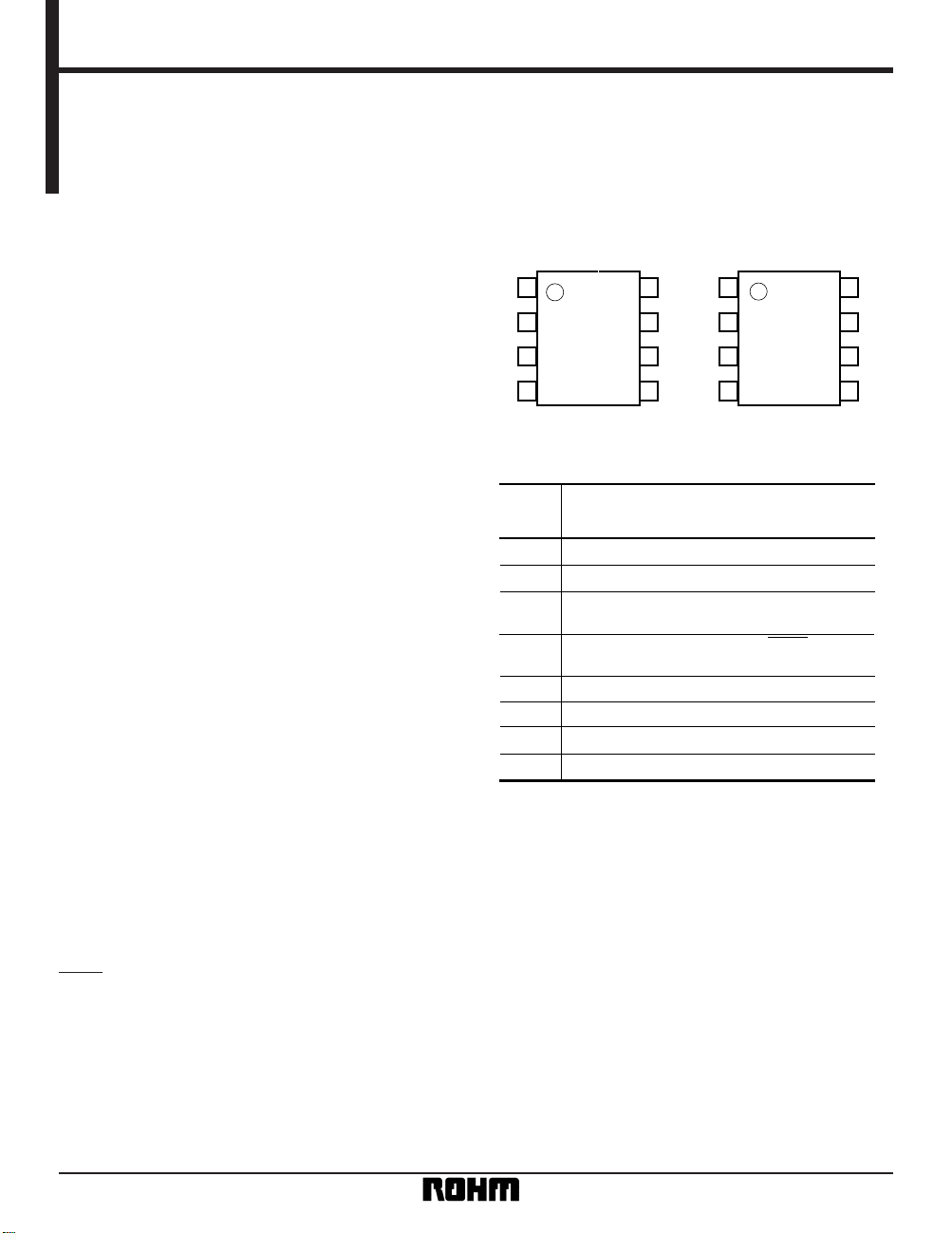
Pin assignments
•
Pin descriptions
1
2
3
4
8
7
6
5
CS
SK
DI
DO
V
CC
N.C.
N.C.
GND
BR93LC66 /
BR93LC66RF
1
2
3
4
8
7
6
5
NC
V
CC
CS
SK
N.C.
GND
DO
DI
BR93LC66F /
BR93LC66FV
CS
SK
DI
DO
GND
N.C.
N.C.
V
CC
Function
Chip select input
Serial clock input
Start bit, operating code, address, and serial
data input
Serial data output, READY / BUSY internal
status display output
Ground
Not connected
Not connected
Power supply
Pin
Name
•
Overview
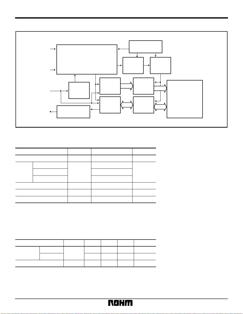
The BR93LC66 series are CMOS serial input / output-type memory circuits (EEPROMs) that can be programmed
electrically. Each is configured of 256 words × 16 bits (4096 bits), and each word can be accessed individually and
data read from it and written to it.
Operation control is performed using five types of commands. The commands, addresses, and data are input
through the DI pin under the control of the CS and SK pins. In a write operation, the internal status signal (READY or
BUSY) can be output from the DO pin.
Page 2
2
Memory ICs BR93LC66 / BR93LC66F / BR93LC66RF / BR93LC66FV
•
Block diagram
16bit
16bit
8bit
4096bit
EEPROM array
CS
SK
DI
DO
8bit
Command code
Control
Clock generation
Command
register
Dummy bit
Address
buffer
Data
register
Power supply
voltage detector
Write disable
High voltage
generator
Address
decoder
R / W
amplifier
•
Absolute maximum ratings (Ta = 25°C)
Parameter Symbol Limits Unit
V
CC – 0.3 ~ + 6.5 V
BR93LC66
Pd
500
∗
1
mW
BR93LC66F / RF
BR93LC66FV
350
∗
2
300
∗
3
Tstg – 65 ~ + 125 °C
Topr – 40 ~ + 85 °C
— – 0.3 ~ V
CC + 0.3 V
Storage temperature
Operating temperature
Terminal voltage
∗
1 Reduced by 5.0mW for each increase in Ta of 1°C over 25°C.
∗
2 Reduced by 3.5mW for each increase in Ta of 1°C over 25°C.
∗
3 Reduced by 3.0mW for each increase in Ta of 1°C over 25°C.
Applied voltage
Power
dissipation
•
Recommended operating conditions (Ta = 25°C)
Parameter Symbol Min. Typ. Max. Unit
V
CC
— 5.5 V
2.0 — 5.5 V
V
IN
0—VCC V
2.7
Input voltage
Writing
Reading
Power supply
voltage
Page 3
3
Memory ICs BR93LC66 / BR93LC66F / BR93LC66RF / BR93LC66FV
•
Electrical characteristics (unless otherwise noted, Ta = – 40 to 85°C, VCC = 5V ± 10%)
Parameter Symbol Min. Typ. Max. Unit Conditions
V
IL – 0.3 — 0.8 V
V
IH 2.0 —
—
—VCC + 0.3 V
V
OL1 — — 0.4 V IOL = 2.1mA
V
OH1 2.4 — — V IOH = – 0.4mA
V
OL2 — — 0.2 V IOL = 10µA
V
OH2 VCC
–
0.4 — — V IOH = – 10µA
I
LI – 1.0 — µAVIN = 0V ~ VCC
ILO – 1.0 — µA
I
CC1
—
1.5 3 mA
I
CC2 — 0.7 1.5 mA
I
SB — 1.0 5 µA
1.0
1.0 V
OUT = 0V ~ VCC, CS = GND
V
IN = VIH / VIL, DO = OPEN, fsk = 1MHz, WRITE
V
IN = VIH / VIL, DO = OPEN, fsk = 1MHz, READ
CS = SK = DI = GND, DO = OPEN
Input low level voltage
Input high level voltage
Output low level voltage 1
Output high level voltage 1
Output low level voltage 2
Output high level voltage 2
Input leakage current
Output leakage current
Standby current
Operating current
dissipation 1
Operating current
dissipation 2
(unless otherwise noted, Ta = – 40 to 85°C, VCC = 3V ± 10%)
Parameter Symbol Min. Typ. Max. Unit Conditions
V
IL
– 0.3 — 0.15 × VCCV
V
IH
0.7 × VCC—VCC + 0.3 V
V
OL
——0.2 VIOL = 10µA
V
OHVCC
– 0.4 — — V IOH = – 10µA
I
LI
– 1.0 — µAVIN = 0V ~ V
CC
I
LO
– 1.0 — µA
I
CC1
— 0.5 2 mA
I
CC2
— 0.2 1 mA
I
SB
— 0.4 3 µA
1.0
1.0 V
OUT
= 0V ~ VCC, CS = GND
CS = SK = DI = GND, DO = OPEN
V
IN
= V
IH
/ VIL, DO = OPEN, fsk = 250kHz, WRITE
V
IN
= VIH / VIL, DO = OPEN, fsk = 250kHz, READ
Input low level voltage
Input high level voltage
Output low level voltage
Output high level voltage
Input leakage current
Output leakage current
Standby current
Operating current
dissipation 1
Operating current
dissipation 2
—
—
•
Electrical characteristics (unless otherwise noted, Ta = – 40 to 85°C, VCC = 2.0V)
Parameter Symbol Min. Typ. Max. Unit Conditions
V
IL
– 0.3 — 0.15 × V
CC
V
V
IH
0.7 × VCC—VCC + 0.3 V
V
OL
——0.2 VIOL = 10µA
V
OHVCC
– 0.4 — — V IOH = – 10µA
I
LI
– 1.0 — 1.0 µAVIN = 0V ~ V
CC
I
LO
– 1.0 — 1.0 µA
I
CC2
— 0.2 1 mA
I
SB
— 0.4 3 µA
V
OUT
= 0V ~ VCC, CS = 0V
CS = SK = DI = 0V, DO = OPEN
V
IN
= VIH / VIL, DO = OPEN, fsk = 200kHz,
READ
Input low level voltage
Input high level voltage
Output low level voltage
Output high level voltage
Input leakage current
Output leakage current
Operating current
dissipation 2
Standby current
—
—
Page 4
4
Memory ICs BR93LC66 / BR93LC66F / BR93LC66RF / BR93LC66FV
(2) Operation timing characteristics
(unless otherwise noted, Ta = – 40 to 85°C, V
CC = 5V ± 10%)
Parameter Symbol Min. Typ. Max. Unit
f
SK — — 1 MHz
t
SKH 450 — — ns
t
SKL 450 — — ns
t
CS 450 — — ns
t
CSS 50 — — ns
t
DIS 100 — — ns
t
CSH 0——ns
t
DIH 100 — — ns
t
PD1 — — 500 ns
t
PD0 — — 500 ns
t
SV — — 500 ns
t
DF — — 100 ns
——10mst
E / W
SK clock frequency
SK "H" time
SK "L" time
CS "L" time
CS setup time
DI setup time
CS hold time
DI hold time
Data "1" output delay time
Data "0" output delay time
Time from CS to output confirmation
Time from CS to output High impedance
Write cycle time
•
Circuit operation
(1) Command mode
With these ICs, commands are not
recognized or acted upon until the
start bit is received. The start bit is
taken as the first “1” that is received
after the CS pin rises.
∗1 After setting of the read command
and input of the SK clock, data corresponding to the specified address is
output, with data corresponding to upper addresses then output in sequence. (Auto increment function)
∗2 When the write or write all addresses command is executed, all data in the selected memory cell is erased automatically, and the input data is written to
the cell.
∗3 These modes are optional modes. Please contact Rohm for information on operation timing.
1 10 A7 ~ A0
1 00 11XXXXXX
1 01 A7 ~ A0 D15 ~ D0
1 00 01XXXXXX D15 ~ D0
1 00 00XXXXXX
1 11 A7 ~ A0
1 00 10XXXXXX
Read (READ)
∗
1
Write Enabled (WEN)
Write (WRITE)
∗
2
Write to All Addresses (WRAL)
∗
2
Write Disabled (WDS)
Erase (ERASE)
∗
3
Chip Erase (ERAL)
∗
3
Command
Start
bit
Operating
code
Address Data
X: Either VIH or V
IL
—
—
—
—
—
Page 5

5
Memory ICs BR93LC66 / BR93LC66F / BR93LC66RF / BR93LC66FV
For low voltage operation (unless otherwise noted, Ta = – 40 to 85°C, VCC = 3V ± 10%)
Parameter Symbol Min. Typ. Max. Unit
f
SK — — 250 kHz
t
SKH 1——µs
t
SKL 1——µs
t
CS 1——µs
t
CSS 200 — — ns
t
DIS 400 — — ns
t
CSH 0——ns
t
DIH 400 — — ns
t
PD1 ——2µs
t
PD0 ——2µs
t
SV ——2µs
t
DF — — 400 ns
——25mst
E / W
SK clock frequency
SK "H" time
SK "L" time
CS "L" time
CS setup time
DI setup time
CS hold time
DI hold time
Data "1" output delay time
Data "0" output delay time
Time from CS to output confirmation
Time from CS to output High impedance
Write cycle time
When reading at low voltage (Unless otherwise noted, Ta = – 40 to 85°C, VCC = 2.0V)
Parameter Symbol Min. Typ. Max. Unit
f
SK — — 200 kHz
t
SKH 2——µs
t
SKL 2——µs
t
CS 2——µs
t
CSS 400 — — ns
t
DIS 800 — — ns
t
CSH 0——ns
t
DIH 800 — — ns
t
PD1 ——4µs
t
PD0 ——4µs
t
DF — — 800 ns
SK clock frequency
SK "H" time
SK "L" time
CS "L" time
CS setup time
DI setup time
CS hold time
DI hold time
Data "1" output delay time
Data "0" output delay time
Time from CS to output High impedance
䊊 Not designed for radiation resistance.
Page 6

6
Memory ICs BR93LC66 / BR93LC66F / BR93LC66RF / BR93LC66FV
(3) Timing chart
CS
SK
DI
DO (READ)
DO (WRITE)
STATUS VALID
tDF
tDFtPD1tPD0
tDIHtDIS
tCSS
tCSH
tSKH tSKL
• Data is acquired from DI in synchronization with the SK rise.
• During a reading operation, data is output from DO in synchronization with the SK rise.
• During a writing operation, a Status Valid (READY or BUSY) is valid from the time CS is HIGH until time tcs after CS falls following the input of a write
command and before the output of the next command start bit. Also, CS must be in a HIGH-Z state when DO is LOW.
• After the completion of each mode, make sure that CS is set to LOW, to reset the internal circuit, before changing modes.
Fig.1 Data synchronization timing
Page 7

7
Memory ICs BR93LC66 / BR93LC66F / BR93LC66RF / BR93LC66FV
CS
SK
DI
DO
∗
1
∗
2
D14
D15
D0
D1
D14
D15
0
High-Z
1
1
00
A7
A6
A1
A0
1
2
411122728
∗
1 If the first data input following the rise of the start bit CS is "1", the start bit is acknowledged. Also, if a "1" is input following several zeroes in succession,
the "1" is recognized as the start bit, and subsequent operation commences. This applies also to all commands described subsequently.
∗
2 Address auto increment function: These ICs are equipped with an address auto increment function which is effective only during reading operations.
With this function, if the SK clock is input following execution of one of the above reading commands, data is read from upper addresses in succession.
CS is held in HIGH state during automatic incrementing.
Fig.2 Read cycle timing (READ)
(4) Reading (Figure 2)
When the read command is acknowledged, the data
(16 bits) for the input address is output serially. The
data is synchronized with the SK rise during A0 acquisition and a “0” (dummy bit) is output. All further data is
output in synchronization with the SK pulse rises.
(5) Write enable (Figure 3)
These ICs are set to the write disabled state by the internal reset circuit when the power is turned on.
Therefore, before performing a write command, the
write enable command must be executed. When this
command is executed, it remains valid until a write
disable command is issued or the power supply is cut
off. However, read commands can be used in either
the write enable or write disable state.
(6) Write (Figure 4)
This command writes the input 16-bit data (D15 to D0)
to the specified address (A7 to A0). Actual writing of
the data begins after CS falls (following the 27th clock
pulse after the start bit input), and DO is in the Acquire
state.
STATUS is not detected if CS = LOW after the time
t
E / W. When STATUS is detected (CS = HIGH), no com-
mands are accepted while DO is LOW (BUSY). Therefore, no commands should be input during this period.
10011
CS
SK
DI
DO
High-Z
Fig.3 Write enable cycle timing
Page 8

8
Memory ICs BR93LC66 / BR93LC66F / BR93LC66RF / BR93LC66FV
CS
SK
DI
DO
High-Z
011
A7 A6 A1 A0
D15 D14 D1 D0
STATUSt
CS
READYBUSY
tSV
tE / W
12 4 1112 27
Fig.4 Write cycle timing (WRITE)
tCS
CS
SK
DI
DO
High-Z
0010
D15 D14 D1 D0
12 5 12 27
STATUS
READYBUSY
tSV
tE / W
Fig.5 Write all address cycle timing (WRAL)
(STATUS)
After time t
CS following the fall of CS, after input of the
write command), if CS is set to HIGH, the write execute
= BUSY (LOW) and the command wait status READY
(HIGH) are output.
If in the command wait status (STATUS = READY), the
next command can be performed within the time t
E / W.
Thus, if data is input via SK and DI with CS = HIGH in
the t
E / W period, erroneous operations may be per-
formed. To avoid this, make sure that DI = LOW when
CS = HIGH. (Caution is especially important when
common input ports are used.) This applies to all of the
write commands.
(7) All address write (Figure 5)
With this command, the input 16-bit data is written
simultaneously to all of the addresses (128 words).
Rather than writing one word at a time, in succession,
data is written all at one time, enabling a write time of
t
E / W.
(8) Write disable (Figure 6)
When the power supply is turned on, the IC enters the
write disable status. Similarly, when a write disable
command is issued, the IC enters the same status.
When in this status, all write commands are ignored,
but read commands may be executed.
In the write enable status, writing begins even if a write
command is entered accidentally. To prevent errors of
this type, we recommend executing a write disable
command after writing has been completed.
10000
CS
SK
DI
DO
High-Z
Fig.6 Write disable cycle timing (WDS)
Page 9

9
Memory ICs BR93LC66 / BR93LC66F / BR93LC66RF / BR93LC66FV
a b
t
E / W
〈WRITE, WRAL〉
〈READ〉
Fig.7
Start bit Operating code Address
Data
1bit 2bits 8bits 16bits
Start bit Operating code Address
Data
1bit 2bits 8bits 16bits
Cancel can be performed for the entire read mode space
Cancellation method: CS LOW
a: Canceled by setting CS LOW or VCC OFF (∗)
b: Cannot be canceled by any method. If V
CC is set to OFF during this time, the data in the
designated address is not secured.
∗
: VCC OFF (VCC is turned off after CS is set to LOW)
•
Operation notes
(1) Cancelling modes
Page 10

10
Memory ICs BR93LC66 / BR93LC66F / BR93LC66RF / BR93LC66FV
(2) Timing in the standby mode
As shown in Figure 8, during standby, if CS rises when
SK is HIGH, the DI state may be read on the rising
edge. If this happens, and DI is HIGH, this is taken to
be the start bit, causing a bit error (see point “a” in
Figure 8).
Make sure all inputs are LOW during standby or when
turning the power supply on or off (see Figure 9).
(3) Precautions when turning power on and off
When turning the power supply on and off, make sure
CS is set to LOW (see Figure 10).
When CS is HIGH, the EEPROM enters the active
state. To avoid this, make sure CS is set to LOW (disable mode) when turning on the power supply.
(When CS is LOW, all input is cancelled.)
When the power supply is turned off, the low power
state can continue for a long time because of the
capacity of the power supply line. Erroneous operations and erroneous writing can occur at such times for
the same reasons as described above. To avoid this,
make sure CS is set to LOW before turning off the
power supply.
To prevent erroneous writing, these ICs are equipped
with a POR (Power On Reset) circuit, but in order to
achieve operation at a low power supply, V
CC is set to
operate at approximately 1.3V. After the POR has been
activated, writing is disabled, but if CS is set to HIGH,
writing may be enabled because of noise or other factors. However, the POR circuit is effective only when
the power supply is on, and will not operate when the
power is off.
Also, to prevent erroneous writing at low voltages,
these ICs are equipped with a built-in circuit (V
CC-lock-
out circuit) which resets the write command if V
CC
drops to approximately 2V or lower (typ.).
(4) Clock (SK) rise conditions
If the clock pin (SK) signal of the BR93LC66 / BR93LC66A has a long rise time (tr) and if noise on the signal
line exceeds a certain level, erroneous operation can
occur due to erroneous counts in the clock. To prevent
this, a Schmitt trigger is built into the SK input of the
BR93LC66. The hysteresis amplitude of this circuit is
set to approximately 0.2V, so if the noise exceeds the
SK input, the noise amplitude should be set to 0.2V
P-P
or lower. Furthermore, rises and falls in the clock input
should be accelerated as much as possible.
(5) Power supply noise
The BR93LC66 discharge high volumes of high voltage
when a write is completed. The power supply may fluctuate at such times. Therefore, make sure a capacitor
of 1000pF or greater is connected between V
CC (Pin 8)
and GND (Pin 5).
SK
CS
DI
ab
01
Fig.8 Timing during erroneous operation
Point a: Start bit position during erroneous operation
Point b: Actual position of start bit
SK
CS
DI
01
b
Fig.9 Timing during normal operation
Good exampleBad example
GND
+ 5V
GND
+ 5V
V
CC
CS
(Bad example) Here, the CS pin is pulled up to VCC. In this case, CS is
HIGH (active state). Please be aware that the EEPROM
may perform erroneous operations or write erroneous
data because of noise or other factors. Also, be aware
that this may occur ever if the CS input is at High-2.
(Good example) In this case, CS is LOW when the power supply is turned
on or off.
Fig.10
Page 11

11
Memory ICs BR93LC66 / BR93LC66F / BR93LC66RF / BR93LC66FV
(6) Connecting DI and DO directly
The BR93LC66 have an independent input pin (DI) and
output pin (DO). These are treated as individual signals
on the timing chart but can be controlled through one
control line.
Control can be initiated on a single control line by
inserting a resistor R.
1) Data collision between the µ-COM output and the
DO output
Within the input and output timing of the BR93LC66 the
drive from the µ-COM output to the DI input and a signal output from the DO output can be emitted at the
same time. This happens only for the 1 clock cycle (a
dummy bit “0” is output to the DO pin) which acquires
the AO address data during a read cycle. When the
address data AO = 1, the µ-COM output becomes a
direct current source for the DO pin.
The resistor R is the only resistance which limits this
current. Therefore, a resistor with a value which satisfies the µ-COM and the BR93LC66 current capacity is
required. When using a single control line, when a
dummy bit “0” is output to the DO, the µ-COM I / O
address data AO is also output. Therefore, the dummy
bit cannot be detected.
2) Feedback to the DI input from the DO output
Data is output from the DO pin and then feeds back
into the DI input through the resistor R. This happens
when:
• DO data is output during a read operation
• A READY / BUSY signal is output during WRITE or
WRAL operation
Such feedback does not cause problems in the basic
operation of the BR93LC66.
The µ-COM input level must be adequately maintained
for the voltage drop at R which is caused by the total
input leakage current for the µ-COM and the BR93LC-
66.
In the state in which SK is input, when the READY /
BUSY function is used, make sure that CS is dropped
to LOW within four clock pulses of the output of the
READY signal HIGH and the standby mode is restored.
For input after the fifth clock pulse, the READY HIGH
will be taken as the start bit and WDS or some other
mode will be activated, depending on the DI state.
µ - COM
I / O PORT
R
DI
DO
BR93LC66
Fig.11 Common connections for
the DI and DO control line
Page 12

12
Memory ICs BR93LC66 / BR93LC66F / BR93LC66RF / BR93LC66FV
•
External dimension (Units: mm)
DIP8
BR93LC66
BR93LC66FV
BR93LC66F / RF
SSOP-B8
SOP8
0.5
±
0.1
3.2
±
0.2 3.4
±
0.3
85
14
9.3
±
0.3
6.5
±
0.3
0.3
±
0.1
0.51Min.
2.54
0°~15°
7.62
0.4 ± 0.11.27
0.15
0.3Min.
0.15 ± 0.1
0.11
6.2 ± 0.3
4.4 ± 0.2
5.0 ± 0.2
85
41
1.5 ± 0.1
0.1
0.22 ± 0.1
0.65
0.3Min.
548
1
6.4 ± 0.3
4.4 ± 0.2
3.0 ± 0.2
1.15 ± 0.1
0.15 ± 0.1
0.1
(0.52)
 Loading...