

Page 1
BR93LC46-W / BR93LC46F-W / BR93LC46RF-W /
Memory ICs
BR93LC46FJ-W / BR93LC46RFJ-W / BR93LC46FV-W
64×16bits serial EEPROM
BR93LC46-W / BR93LC46F-W / BR93LC46RF-W /
BR93LC46FJ-W / BR93LC46RFJ-W / BR93LC46FV-W
The BR93LC46-W series are CMOS serial input / output-type memory circuits (EEPROMs) that can be programmed
electrically. Each is configured of 64 words × 16 bits (1,024 bits), and each word can be accessed individually and data
read from it and written to it. Operation control is performed using five types of commands.
The commands, addresses, and data are input through the DI pin under the control of the CS and SK pins. In a write
operation, the inter nal stat us si gnal (READ Y or BUSY) can be o utput fro m th e DO pin.
z
zApplications
zz
VCRs, TVs, printers, car stereos, cordless telephones, short wave radios, programmable DIP switches, and
other battery-powered equipment requiring low voltage and low current
z
zFeatures
zz
1) 64 words × 16 bits EEPROM
2) Operati ng v oltag e ran ge
When reading : 2.0 to 5.5V
When writing : 2.7 to 5.5V
3) Low current consumption
Operating (at 5V) : 3mA (Max .)
Standby (at 5V) : 5µA (M ax.)
4) Address can be incremented automatically during
read operations.
5) Auto erase and auto complete functions can be used
during write operations.
6) A write instru ction i nhibit function allow s :
- write protection when power supply voltage is low.
- write disable state at power up.
- writing using command codes.
7) Compact packages
8) Display of READY / BUSY stat us
9) TTL-compatible input / output
10) Rewriting possible up to 100,000 times
11) Data can be stored for ten years without corruption.
zzzz
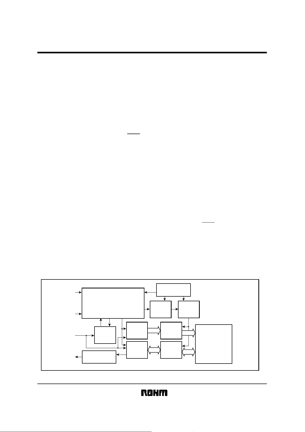
Block diagram
DO
Power supply
CS
SK
DI
Command decode
Control
Clock generation
Command
register
Dummy bits
Address
buffer
Data
register
6bits
16bits
voltage detector
Write
disable
Address
decoder
R / W
amplifier
High voltage
generator
6bits
1,024bits
EEPROM array
16bits
Page 2
Memory ICs
z
zPin descriptions
zz
BR93LC46-W / BR93LC46F-W / BR93LC46RF-W /
BR93LC46FJ-W / BR93LC46RFJ-W / BR93LC46FV-W
CS
1
SK
2
BR93LC46-W
V
8
N.C.
7
BR93LC46RF-W
BR93LC46RFJ-W
DI
DO
3
4
Fig.1
6
N.C.
5
GND
Pin No.
BR93LC46-W
BR93LC46RF-W
BR93LC46RFJ-W
BR93LC46F-W
BR93LC46FJ-W
BR93LC46FV-W
13CS
24SK
35DI
46DO
5 7 GND
6 8 N.C.
7 1 N.C.
82V
zzzz
Absolute maximum ratings
(T a = 2 5°C)
Parameter
Applied voltage
BR93LC46-W
Power
dissipation
BR93LC46FV-W
Storage temperature
Operating temperature
Terminal voltage
∗1 Reduced by 5.0mW for each increase in Ta of 1°C over 25°C.
∗2 Reduced by 3.5mW for each increase in Ta of 1°C over 25°C.
∗3 Reduced by 3.0mW for each increase in Ta of 1°C over 25°C.
CC
N.C.
V
1
CC
2
BR93LC46F-W
N.C.
8
GND
7
BR93LC46FJ-W
BR93LC46FV-W
Pin
name
3
CS
4
SK
Fig.2
Function
6
DO
5
DI
Chip select input
Serial clock input
Start bit, operating code, address, and seria data input
Serial data output, READY / BUSY internal status display output
Ground
Not connected
Not connected
CC
Power supply
Symbol
V
CC
Pd
Tstg
Topr
−
Limits Unit
−0.3~+6.5
∗1
500
∗2
∗3
300
~+
125
−65
~+
85
−40
~
V
CC
+
−0.3
0.3
V
mWBR93LC46F-W / RF-W / FJ-W / RFJ-W 350
°C
°C
V
z
zRecommended operating conditions (T a = 25°C)
zz
Parameter Symbol Min. Typ. Max. Unit
Power supply
voltage
Input voltage
Writing
Reading
V
CC
V
IN
2.7
2.0 − 5.5 V
0 − V
− 5.5 V
CC
V
Page 3
BR93LC46-W / BR93LC46F-W / BR93LC46RF-W /
Memory ICs
z
zElectrical characteristics
zz
For 5V operation (unless otherwise noted, Ta = −40 to + 85°C, V
Parameter
Input low level voltage
Input high level voltage
Output low level voltage 1
Output high level voltage 1
Output low level voltage 2
Output high level voltage 2
Input leakage current
Output leakage current
Operating current
dissipation 1
Operating current
dissipation 2
Standby current
For 3V operation (unless otherwise noted, Ta = −40 to + 85°C, VCC = 3.0V ± 10%)
Parameter Symbol Min. Typ. Max. Unit Conditions
Input low level voltage
Input high level voltage
Output low level voltage
Output high level voltage
Input leakage current
Output leakage current
Operating current
dissipation 1
Operating current
dissipation 2
Standby current
BR93LC46FJ-W / BR93LC46RFJ-W / BR93LC46FV-W
= 5.0V ± 10%)
CC
Symbol Min. Typ. Max. Unit Conditions
V
IL
−0.3 −
IH
V
V
V
V
V
I
I
I
CC1
I
CC2
I
V
IL
V
IH
OL
V
V
OH
I
LI
I
LO
I
CC1
CC2
I
I
SB
2.0
OL1
OH1
OL2
OH2
LI
LO
SB
−−
2.4
−−
VCC−0.4 −
−1.0 −µAVIN=0V~V
−1.0 −µAV
1.5 3.0 mA
−
0.7 1.5 mA
−
1.0 5.0
−
−0.3 −
0.7×V
CC
−
−−0.2 V IOL=10µA
VCC−0.4 −−VIOH=−10µA
−1.0 −µAVIN=0V~V
−1.0 −µA
− 0.5 2.0 mA
− 0.2 1.0 mA
0.4 3.0
−
0.8 V
−−
V
CC
0.4 V
−−
0.2 V
− V
V
+
0.3
IOL=2.1mA
V
OH
=−0.4mA
I
IOL=10µA
IOH=−10µA
1.0
1.0
OUT
=0V~VCC, CS=GND
VIN=VIH / VIL, DO=OPEN,
f=1MHz, WRITE
V
IN=VIH
/ VIL, DO=OPEN,
f=1MHz, READ
µACS=SK=DI=GND, DO=OPEN
0.15×V
CC
V
CC
+
0.3 V
1.0
1.0
OUT
=0V~VCC, CS=GND
V
V
IN=VIH
/ VIL, DO=OPEN
f=250kHz, WRITE
V
IN=VIH
/ VIL, DO=OPEN
f=250kHz, READ
µACS=SK=DI=GND, DO=OPEN
Measurement circuit
−
−
−
Fig.3
Fig.4
Fig.3
Fig.4
CC
Fig.5
Fig.6
Fig.7
Fig.7
Fig.8
Measurement circuit
−
−V
−
−
Fig.3
Fig.4
CC
Fig.5
Fig.6
Fig.7
Fig.7
Fig.8
For 2V operation (unless otherwise noted, Ta = −40 to + 85°C, VCC = 2.0V)
Parameter Symbol Min. Typ. Max. Unit Conditions
Input low level voltage
Input high level voltage
Output low level voltage
Output high level voltage
Input leakage current
Output leakage current
Operating current
dissipation 2
Standby current
V
IL
−0.3 −
V
IH
0.7×V
CC
V
OL
V
OH
I
LI
I
LO
I
CC2
SB
I
−−0.2 V IOL=10µA
VCC−0.4 −−VIOH=−10µA
−1.0 −µAVIN=0V~V
−1.0 −µA
− 0.2 1.0 mA
−
0.4
0.15×V
CC
−
CC
+
0.3 V
1.0
1.0
3.0
V
V
V
f=200kHz, READ
µA
CS=SK=DI=GND, DO=OPEN
−
−V
CC
OUT
=0V~VCC, CS=GND
IN=VIH
/ VIL, DO=OPEN
Measurement circuit
−
−
Fig.3
Fig.4
Fig.5
Fig.6
Fig.7
Fig.8
Page 4
Memory ICs
z
zMeasurement circuits
zz
BR93LC46-W / BR93LC46F-W / BR93LC46RF-W /
BR93LC46FJ-W / BR93LC46RFJ-W / BR93LC46FV-W
V
V
GND
CC
CC
DO
VV
I
OL
OL
V
V
GND
CC
CC
DO
VV
I
OH
OH
VIN=0~V
SK
=1MHz / 250kHz / 200kHz
f
V
IN=VIH
/ V
IL
WRITE / READ INPUT
CS,SK,DI
CS
SK
DI
Control output to "LOW"
V
CC
A
V
CC
GND
Fig.3 "LOW" output voltage circuit
I
LI
A
CC
Fig.5 Input leak current circuit
Fig.7 Supply current circuit
V
V
GND
CC
CC
I
CC
DO OPEN
Control output to "HIGH"
Fig.4 "HIGH" output voltage circuit
V
CC
V
CC
GND
Fig.6 Output leak current circuit
Vcc
A
Vcc
CS
SK
DI
GND
Fig.8 Standby current circuit
I
LO
DOCS
A
SB
I
DO
OPEN
VO=0~V
CC
zzzz
Circuit operation
(1) Command mode
With these ICs, commands are not recognized or acted upon until the start bit is received. The start bit is taken as
the first “1” that is received after the CS pin rises.
Start
Command
Read (READ)
∗1
Write enabled (WEN)
Write (WRITE)
Write all addresses (WRAL)
∗2
∗2
Write disabled (WDS)
Erase (ERASE)
Chip erase (ERAL)
X: Either VIH or V
∗1 After setting of the read command and input of the SK clock, data corresponding to the specified address is output,
with data corresponding to upper addresses then output in se-quence. (Auto increment function)
∗2 When the write or write all addresses command is executed, all data in the selected memory cell is erased
autematically, and the input data is writen to the cell.
∗3 These modes are optinal modes. Please contact Rohm for information on operation timing.
∗3
∗3
IL
Operating
bit
110
100
1 01 D15
1 00 D15
100
111
100
code
Address Data
A5~A0
11XXXX
−
−
A5~A0
01XXXX
00XXXX
A5~A0
10XXXX
−
−
−
~
D0
~
D0
Page 5

BR93LC46-W / BR93LC46F-W / BR93LC46RF-W /
Memory ICs
(2) Operation timing characteristics
For 5V operation (unless otherwise noted, Ta = −40 to + 85°C, V
Parameter
SK clock frequency
SK "HIGH" time
SK "LOW" time
CS "LOW" time
CS setup time
DI setup time
CS hold time
DI hold time
Data "1" output delay time
Data "0" output delay time
Time from CS to output confirmation
Time from CS to output High impedance
Write cycle time
For low voltage operation (unless otherwise noted, Ta = −40 to + 85°C, VCC = 3.0V ± 10%)
Parameter Symbol Min. Typ. Max. Unit
SK clock frequency
SK "HIGH" time
SK "LOW" time
CS "LOW" time
CS setup time
DI setup time
CS hold time
DI hold time
Data "1" output delay time
Data "0" output delay time
Time from CS to output confirmation
Time from CS to output High impedance
Write cycle time
BR93LC46FJ-W / BR93LC46RFJ-W / BR93LC46FV-W
= 5.0V ± 10%)
CC
Symbol Min. Typ. Max. Unit
SK
t
t
t
t
t
t
t
t
t
t
t
t
t
t
f
SKH
SKL
t
CS
CSS
DIS
t
CSH
t
DIH
PD1
PD0
t
SV
DF
t
E / W
f
SK
SKH
SKL
t
CS
CSS
t
DIS
CSH
t
DIH
PD1
PD0
t
SV
DF
t
E / W
−−
450
450
450
50
100
0
100
−−
−−
−−
−−
−−
−−
−−
−−
−−
−−
−−
−−
−−
1
1
1
200
400
0
400
−−µs
−−µs
−−µs
−−
−−
−−
−−
−−
−−
−−
−−
−−
1 MHz
ns
ns
ns
ns
ns
ns
ns
500 ns
500 ns
500 ns
100 ns
10 ms
250 kHz
ns
ns
ns
ns
2
2
2
µs
µs
µs
400 ns
25 ms
When reading at low voltage (unless otherwise noted, T a = −40 to + 85°C, VCC = 2.0V)
Parameter Symbol Min. Typ. Max. Unit
t
t
t
t
t
t
f
SKH
t
CSS
t
CSH
t
t
SK
SKL
CS
DIS
DIH
PD1
PD0
DF
−−
2
2
2
400
800
0
800
−−µs
−−µs
−−µs
−−
−−
−−
−−
−−
−−
−−
200 kHz
ns
ns
ns
ns
4
4
µs
µs
800 ns
SK clock frequency
SK "HIGH" time
SK "LOW" time
CS "LOW" time
CS setup time
DI setup time
CS hold time
DI hold time
Data "1" output delay time
Data "0" output delay time
Time from CS to output High impedance
Not designed for radiative rays.
Page 6

BR93LC46-W / BR93LC46F-W / BR93LC46RF-W /
Memory ICs
(3) Timing chart
·
Data is acquired from DI in synchronization with the SK rise.
·
During a reading operation, data is output from DO in synchronization with the SK rise.
·
During a writing operation, a Status Valid (READY or BUSY) is valid from the time CS is HIGH until time tCS after CS falls following the input of
a write command and before the output of the next command start bit. Also, DO must be in a HIGH-Z state when CS is LOW.
·
After the completion of each mode, make sure that CS is set to LOW, to reset the internal circuit, before changing modes.
BR93LC46FJ-W / BR93LC46RFJ-W / BR93LC46FV-W
CS
t
DO (READ)
DO (WRITE)
CSS
SK
t
DIS
DI
t
SKH
t
DIH
t
PD0
t
SKL
STATUS VALID
t
PD1
t
CSH
t
DF
t
DF
Fig.9 Synchronized data timing
(4) Reading (Fig.10)
When the read command is acknowledged, the data (16 bits) for the input address is output serially. The data is
synchronized with the SK rise during A0 acquisition and a “0” (dummy bit) is output. All further data is output in
synchroniz ati on w ith t he S K pu lse rise s.
CS
SK
DI
DO
(
1) If the first data input following the rise of the start bit CS is "1", the start bit is acknowledged. Also, if a "1" is input following several zeroes in succession, the
∗
"1" is recognized as the start bit, and subsequent operation commences. This applies also to all commands described subsequently.
(∗2) Address auto increment function: These ICs are equipped with an address auto increment function which is effective only during reading operations. With
this function, if the SK clock is input following execution of one of the above reading commands, data is read from upper addresses in succession.
CS is held in HIGH state during automatic incrementing.
1)
(
∗
1 2 4 9 10 25 26
A5
High Z
110
A4
A0
A1
D15
0
D14
Fig.10 Read cycle timing (READ)
2)
(
∗
D1
D0
D14D15
Page 7

BR93LC46-W / BR93LC46F-W / BR93LC46RF-W /
Memory ICs
(5) Write enable (Fig.11)
These ICs are set to the write disabled state by the internal reset circuit when the power is turned on. Therefore,
before performing a write command, the write enable command must be executed. When this command is
executed, it remains valid until a write disable command is issued or the power supply is cut off. However, read
commands can be used in either the write enable or write disable state.
BR93LC46FJ-W / BR93LC46RFJ-W / BR93LC46FV-W
CS
SK
DI
DO
10011
High Z
Fig.11 Write enable cycle timing
(6) Write (Fig.12)
This command writes the input 16 bits data (D15 to D0) to the specified address (A5 to A0). Actual writing of the data
begins after CS falls (following the 25th clock pulse after the start bit input), and D0 is in the Acquire state.
STATUS is not detected if CS = LOW after the time t
. When STA TUS is detected (CS = HIGH), no commands are
E / W
accepted while DO is LOW (BUSY). Therefore, no commands should be input during this period.
CS
1
SK
DI
DO
High Z
24 910 25
011
A5 A4 A1 A0
D15 D14 D1 D0
Fig.12 Write cycle timing (WRITE)
CS
STATUSt
SV
t
READYBUSY
t
E / W
(ST ATUS)
After time tCS fo llowin g the fall of CS, after input of th e write co mmand) , if CS is set to HIGH, the w rite ex ecute = BUSY
(LOW) and the command wait status READY (HIGH) are output.
If in the command wait status (ST ATUS = READY), the next command can be performed within the time t
data is input via SK and DI with CS = HIGH in the t
period, erroneous operations may be performed. To avoid this,
E / W
E / W
. Thus, if
make sure that DI = LOW when CS = HIGH. (Caution is especially important when common input ports are used.) This
applies to all of the write commands.
Page 8

BR93LC46-W / BR93LC46F-W / BR93LC46RF-W /
Memory ICs
(7) All address write (Fig.13)
With this command, the input 16 bits data is written simultaneously to all of the addresses (64 words). Rather than
writing one word at a time, in succession, data is written all at one time, enabling a write time of t
CS
BR93LC46FJ-W / BR93LC46RFJ-W / BR93LC46FV-W
.
E / W
SV
t
STATUS
SK
DI
DO
High Z
12 5 10 25
00101
D15 D14 D1 D0
CS
t
READYBUSY
t
E / W
Fig.13 Write all address cycle timing. (WRAL)
(8) Write di sable (F ig.14)
When the power supply is turned on, the IC enters the write disable status. Similarly, when the write disable command
is issued, the IC enters the same status. When in this status, all write commands are ignored, but read commands
may be executed.
In the write enable status, writing begins even if a write command is entered accidentally. To prevent errors of this type,
we recommend executing a write disable command after writing has been completed.
CS
SK
DI
DO
1 0000
High Z
Fig.14 Write disable cycle timing (WDS)
z
zOperation notes
zz
(1) Cancelling modes
〈READ〉
Start bit Operating code Address Data
1 bit 2 bits 6 bits 16 bits
Cancel can be performed for the entire read mode space
〈WRITE, WRAL〉
Start bit
1 bit 2 bits 6 bits 16 bits
a: Canceled by setting CS LOW or V
b: Cannot be canceled by any method. If V
designated address is not secured.
VCC OFF (VCC is turned off after CS is set to LOW)
∗
Cancellation method: CS LOW
Operating code Address Data
a b
CC
OFF (∗)
CC
is set to OFF during this time, the data in the
Fig.15
t
E / W
Page 9

BR93LC46-W / BR93LC46F-W / BR93LC46RF-W /
Memory ICs
(2) Timing in the standby mode
As shown in Fig.16, during standby, if CS rises when SK is HIGH, the DI state may be read on the rising edge. If this
happens, and DI is HIGH, this is taken to be the start bit, causing a bit error (see point “a” in Fig.16).
Make sure all inputs are LOW during standby or when turning the power supply on or off (see Fig.17).
Point a: Start bit position during erroneous operation
Point b: Timing during normal operation
BR93LC46FJ-W / BR93LC46RFJ-W / BR93LC46FV-W
SK
CS
DI
01
ab
Fig. 16 Erroneous operation timing
SK
CS
DI
Fig. 17 Normal operation timing
01
b
(3) Precautions when turning power on and off
When turning the power supply on and off, make sure CS is set to LOW (see Fig.18).
When CS is HIGH, the EEPROM enters the active state. T o avoid this, make sure CS is set to LOW (disable mode)
when turning on the power supply. (When CS is LOW, all input is cancelled.)
When the power supply is turned off, the low power state can continue for a long time because of the capacity of the
power supply line. Erroneous operations and erroneous writing can occur at such times for the same reasons as
described above. To avoid this, make sure CS is set to LOW before turning off the power supply.
To prevent erroneous writing, these ICs are equipped with a POR (Power On Reset) circuit, but in order to achieve
operation at a low power supply, V
is set to operate at approximately 1.3V. After the POR has been activated,
CC
writing is disabled, but if CS is set to HIGH, writing may be enabled because of noise or other factors. However, the
POR circuit is effective only when the power supply is on, and will not operate when the power is off.
Also, to prevent erroneous writing at low voltages, these ICs are equipped with a built-in circuit (V
which resets the writ e comman d if V
drops to approximately 2V or lower (typ.) (∗).
CC
-lockout circuit)
CC
+ 5V
V
CC
GND
+ 5V
CS
(Bad example)
(Good example)
GND
Here, the CS pin is pulled up to VCC. In this case,
CS is HIGH (active state). Please be aware that the EEPROM may
perform erroneous operations or write erroneous data because of
noise or other factors. Please be aware that this can occur even if
the CS input is HIGH-Z.
In this case, CS is LOW when the power supply is turned
on or off.
Good exampleBad example
Fig. 18
(4) Clock (SK) rise conditions
If the clock pin (SK) signal of the BR93LC46-W has a long rise time (tr) and if noise on the signal line exceeds a
certain level, erroneous operation can occur due to erroneous counts in the clock. T o prevent this, a Schmitt trigger is
built into the SK input of the BR93LC46-W. The hysteresis amplitude of this circuit is set to approximately 0.2V , so if
the noise exceeds the SK input, the noise amplitude should be set to 0.2V
or lower. Furthermore, rises and falls in
P-P
the clock input sh ould be a cceler ated a s much a s possibl e.
Page 10

BR93LC46-W / BR93LC46F-W / BR93LC46RF-W /
Memory ICs
(5) Power supply noise
The BR93LC46-W discharge high volumes of high voltage when a write is completed. The power supply may
fluctuate at such times. Therefore, make sure a capacitor of 1000pF or greater is connected between V
GND (Pin 5).
(6) Connecting DI and DO directly
The BR93LC46-W have an independent input pin (DI) and output pin (DO). These are treated as individual signals
on the timing chart but can be controlled through one control line. Control can be initiated on a single control line by
inserting a resistor R.
BR93LC46FJ-W / BR93LC46RFJ-W / BR93LC46FV-W
(Pin 8) and
CC
µCOM
IO port
R
Fig. 19 Common connections for the DI and DO control line
BR93LC46
DI
DO
1) Data collision between the µ-COM output and the DO output
Within the input and output timing of the BR93LC46-W the drive from the µ-COM output to the DI input and a signal
output from the DO output can be emitted at the same time. This happens only for the 1 clock cycle (a dummy bit
“0” is output to the DO pin) which acquires the A0 address data during a read cycle.
When the address data A0 = 1, the µ-COM output becomes a direct current source for the DO pin. The resistor R
is the only re sista nce w hi ch lim its thi s cur ren t. The ref ore, a re sist or w ith a val ue w hich sati sfie s th e µ-COM and the
BR93LC46-W current capacity is required. When using a single control line, when a dummy bit “0” is output to the
DO, the µ-COM I / O address data A0 is also output. Therefore, the dummy bit cannot be detected.
2) Feedback to the DI input from the DO output
Data is output from the DO pin and then feeds back into the DI input through the resistor R. This happens when:
•
DO data is output during a read operation
•
A READY / BUSY sign al is outp ut du ring WRITE or WRAL ope rati on
Such feedback does not cause problems in the basic operation of the BR93LC46-W.
The µ-COM input level must be adequately maintained for the voltage drop at R which is caused by the total input
leakage current for the µ-COM and the BR93LC46-W. In the state in which SK is input, when the READY / BUSY
function is used, make sure that CS is dropped to LOW within four clock pulses of the output of the READY signal
HIGH and the standby mode is restored. For input after the fifth clock pulse, the READY HIGH will be taken as the
start bit and WDS or some other mode will be activated, depending on the DI state.
Page 11

BR93LC46-W / BR93LC46F-W / BR93LC46RF-W /
Memory ICs
z
zExternal dimensions (Units : mm)
zz
BR93LC46FJ-W / BR93LC46RFJ-W / BR93LC46FV-W
BR93LC46-W
9.3 ± 0.3
85
14
0.51Min.
2.54
3.2± 0.2 3.4 ± 0.3
BR93LC46FJ-W / RFJ-W
4.9 ± 0.2
85
76
6.0 ± 0.3
3.9 ± 0.2
4123
1.375 ±0.1
0.175
1.27
0.5 ± 0.1
0.42 ± 0.1
0.1
6.5 ± 0.3
0°~15°
DIP8
0.45Min.
SOP-J8
7.62
BR93LC46F-W / RF-W
5.0 ± 0.2
85
4.4 ± 0.2
6.2 ± 0.3
1.5 ± 0.1
0.3 ± 0.1
0.11
1.27
41
0.4 ± 0.1
0.15 ± 0.1
0.3Min.
0.15
SOP8
BR93LC46FV-W
3.0 ± 0.2
548
6.4 ± 0.3
4.4 ± 0.2
0.2 ± 0.1
(0.52)
1
0.22 ± 0.1
1.15 ± 0.1
0.1
0.65
0.3Min.
0.15 ± 0.1
0.1
SSOP-B8
 Loading...