

Page 1
A
Universal Standard Specification Series Serial EEPROM Series
Advantage Series Serial EEPROMs
Microwire BUS
BR93C□□-10□U-2.7 family
●Description
The BR93C46/56/66/76/86 series ICs are serial EEPROMs of 1K/2K/4K/8K/16Kbits, respectively, that feature low voltage
operation and low power consumption, enabling compatibility with a wide range of applications. In addition, compact
packages are available, contributing to end-product miniaturization.
●Features
Microwire Bus interface
Single supply voltage: 2.7 to 5.5V
16bit serial EEPROM
Automatic ERASE before WRITE and self-timed programming cycle
Ready /Busy status
2MHz Clock Frequency, 10ms WRITE Time
Auto-increment of register address for READ mode
1,000,000 WRITE/ERASE Cycles
40-year data retention
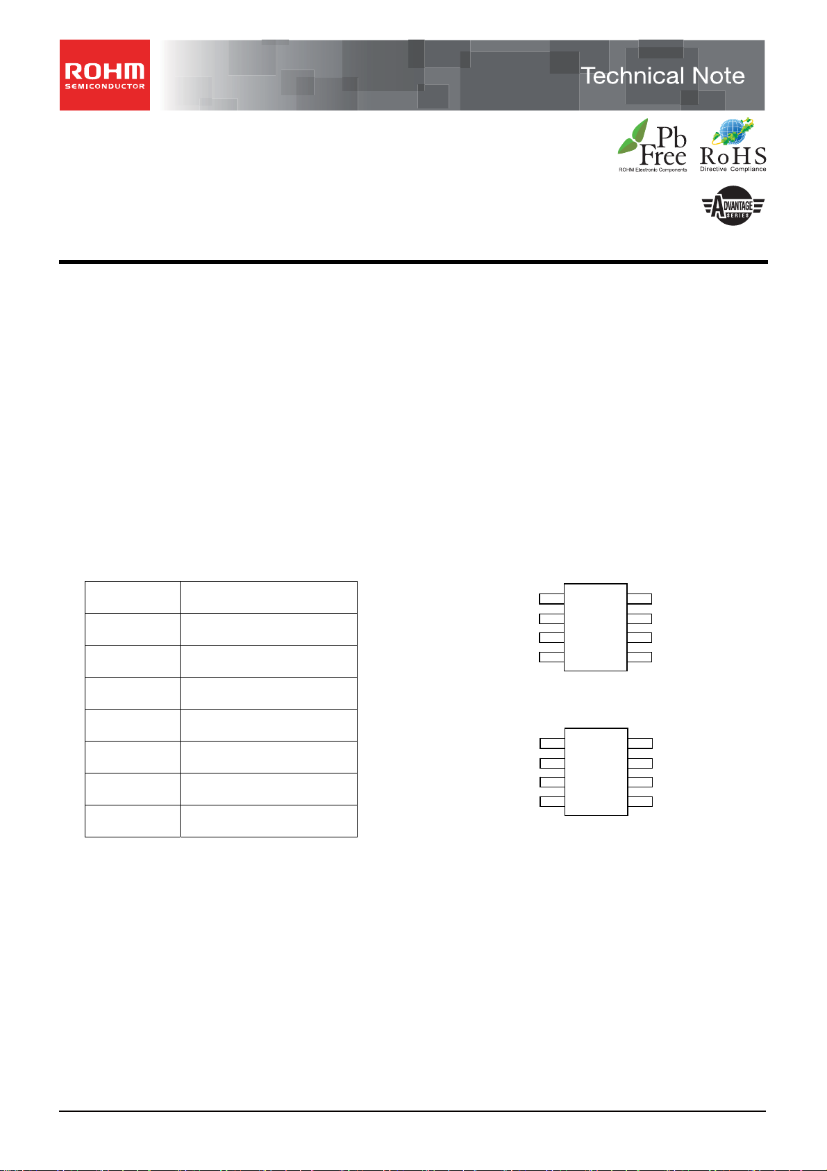
●Pin configuration
Table1.Pin Configurations
Pin Name Function
CS Chip Select
SK Serial Data Clock
DI Serial Data Input
DO Serial Data Output
GND Ground
VCC Power Supply
DC Don’t Connect
These EEPROMs utilize a three line serial interface
consisting of Serial Data Input (DI), Serial Clock (SK), and
Serial Data Output (DO)
After one READ instruction segment is received, if the Chip
Select (CS) remains HIGH, the address pointer
automatically cycles to the next higher register address,
giving a continuous string of output data, depending on the
device and the starting address.
When a WRITE or WRAL instruction is received, the
previous data in the address locations are automatically
overwritten, eliminating the need for an ERASE command.
When Chip Select (CS) is set to H after the WRITE
command, the Status signal (Ready/Busy) becomes active
at the Serial Data Output (DO) until the start bit of the next
command. The Status signal is active when Chip Select (CS)
is HIGH, and Serial Data Output (DO) pin outputs High – Z
when Chip Select (CS) is LOW.
CS
SK
DI
DO
8-lead SOIC Rotated (1K JEDEC only)
DC
VCC
CS
SK
8-lead SOIC
1
2
3
4
1
2
3
4
Figure1.Package
8
7
6
5
8
7
6
5
No.10001EAT12
VCC
DC
DC
GND
DC
GND
DO
DI
www.rohm.com
© 2010 ROHM Co., Ltd. All rights reserved.
1/9
2010.07 - Rev.
Page 2
A
t
t
BR93C□□-10□U-2.7 family
●Absolute maximum ratings
Table 2: Absolute Maximum Ratings
Parameter Symbol
Ratings
Min. Max.
Unit
Technical Note
Storage Temperature T
Output Range(Q=V
or Hi-Z) V
OH
-65 125 ℃
STG
-0.3 Vcc+0.3 V
out
Input range VIN -0.3 VCC+0.3 V
Supply Voltage VCC -0.3 6.5 V
●Recommended Operating Conditions
Table 3: Recommended Operating Conditions
Parameter Symbol
Supply Voltage VCC
Ambient Operating Temperature TA
Ratings
Min. Max.
2.7 5.5 V
-40 85 ℃
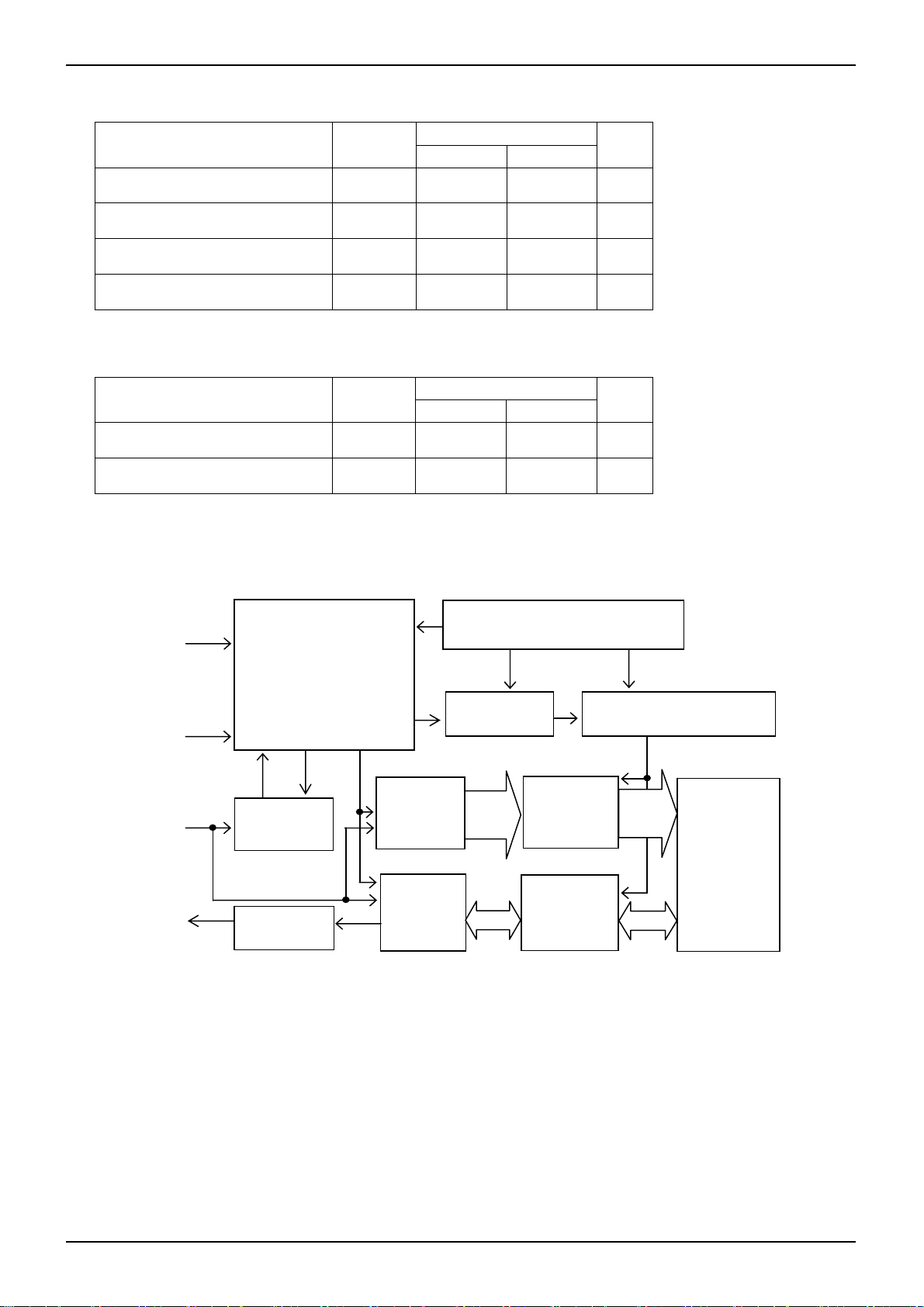
●Block Diagram
Power Source Voltage Detection
CS
Command Decode
Control
Clock Generation
Unit
SK
DI
Command
Register
Address
Buffer
Write
Prohibit
6bi
7bit
8bit
9bit
10bit
Address
Decoder
High Voltage
6bi
7bit
8bit
9bit
10bit
1024 bit
2048 bit
4096 bit
8192 bit
16384 bit
DO
Dummy Bit
Data
Register
16bit
R/W
Amplifier
16bit
EEPROM
Figure 2: Block Diagram
www.rohm.com
© 2010 ROHM Co., Ltd. All rights reserved.
2/9
2010.07 - Rev.
Page 3

A
BR93C□□-10□U-2.7 family
●Electrical characteristics
Table 4: DC Characteristics (Unless otherwise specified, Ta=-40-85℃, VCC=2.7-5.5V)
Parameter Symbol
Min. Typ. Max.
Limits
Unit Test Condition
Supply Voltage VCC 2.7 - 5.5 V
Technical Note
Supply Current ICC
Standby Current ISB
- - 2.0 mA VCC=5V, READ at f=1MHz
- - 2.0 mA VCC=5V, WRITE at f=1MHz
- - 10 µA Vcc=2.7V,CS=0V
- - 30 µA Vcc=5.0V,CS=0V
Input Leakage IIL - - 1.0 µA 0V≦VIH≦Vcc
Output Leakage IOL - - 1.0 µA 0≦V
Input Low Voltage
Input High Voltage
Input Low Voltage
Input High Voltage
Output Low Voltage
Output High Voltage
V
IL1
V
IH1
V
IL2
V
IH2
V
OL1
V
OH1
-0.3
2.0
-0.3
0.7VCC
- - 0.4 V
2.4 - - V
0.8V
+0.3
0.2V
V
CC
CC
CC
+0.3
V 4.0V≦VCC≦5.5V
V VCC≦4.0V
2.7V≦V
I
OL
Table 5: AC Characteristics (Unless otherwise specified, Ta=-40-85℃, V
0
0
250
250
250
250
250
250
50
50
100
100
Specification
-
-
-
-
-
-
-
-
-
-
-
-
Parameter
SK Clock Frequency
SK High Time
SK Low Time
Minimum CS Low Time
CS Set-up Time(relative to SK)
DI Set-up Time(relative to SK)
Symbol
fSK
*1
t
SKH
*1
t
SKL
tCS
t
CSS
t
DIS
Min. Typ. Max
=2.7-5.5V)
CC
2
1
-
-
-
-
-
-
-
-
-
-
Unit
MHz
ns
ns
ns
ns
ns
4.5V≦Vcc≦5.5V
2.7V≦Vcc≦5.5V
4.5V≦Vcc≦5.5V
2.7V≦Vcc≦5.5V
4.5V≦Vcc≦5.5V
2.7V≦Vcc≦5.5V
4.5V≦Vcc≦5.5V
2.7V≦Vcc≦5.5V
4.5V≦Vcc≦5.5V
2.7V≦Vcc≦5.5V
4.5V≦Vcc≦5.5V
2.7V≦Vcc≦5.5V
OUT≦VCC
,DO in Hi-Z
≦5.5V
CC
=2.1mA, IOH=-0.4mA
Te st Condition
CS Hold Time(relative to SK)
DI Hold Time(relative to SK)
Output Delay to “1”
Output Delay to “0”
CS to Status Vaid
CS to Do in High Impedance
Write Cycle time
Endurance(5.0V,25℃)
*1: t
+ t
≧1/fc
SKH
SKL
www.rohm.com
© 2010 ROHM Co., Ltd. All rights reserved.
t
0 - - ns
CSH
DIH
t
PD1
t
PD0
- -
t
SV
- -
t
DF
100
- -
- -
100
t
-
-
-
-
250
250
250
250
250
250
100
100
4.5V≦Vcc≦5.5V
ns
2.7V≦Vcc≦5.5V
4.5V≦Vcc≦5.5V
ns
2.7V≦Vcc≦5.5V
4.5V≦Vcc≦5.5V
ns
2.7V≦Vcc≦5.5V
4.5V≦Vcc≦5.5V
ns
2.7V≦Vcc≦5.5V
4.5V≦Vcc≦5.5V
ns
2.7V≦Vcc≦5.5V
tWP - - 10 ms
- 1M - -
Write
Cycle
3/9
2010.07 - Rev.
Page 4

A
BR93C□□-10□U-2.7 family
●Operating Instructions
The BR93□□ has a seven instruction set, shown in Tables
6, 7 and 8. The timing charts depicted in Figures 3 to 10.
Input Data are clocked in from Serial Data Input (DI) at the
rising edge of the Serial Clock (SK), while output data from
The EEPROM recognizes the first 1 data received, after
Chip Select (CS) goes HIGH, as the START bit. The input of
many 0’s before 1 will not make a difference – 1 will still be
recognized as the START bit.
the Serial Data Output (DO) toggles at the rising edge of the
Serial Clock (SK) during READ mode.
Table 6: Instruction Set (BR93C46)
Instruction Start Bit Op Code Address*1 Data
READ 1 10 A5 A4 A3 A2 A1 A0
EWEN 1 00 1 1 * * * *
ERASE 1 11 A5 A4 A3 A2 A1 A0
WRITE 1 01 A5 A4 A3 A2 A1 A0 D15~D0
ERAL 1 00 1 0 * * * *
WRAL 1 00 0 1 * * * * D15~D0
EWDS 1 00 0 0 * * * *
*1: * = Inconsequential bit
Table 7: Instruction Set (BR93C56 and BR93C66)
*1, *2
Instruction Start Bit Op Code Address
Data
Technical Note
READ 1 10 A7 A6 A5 A4 A3 A2 A1 A0
EWEN 1 00 1 1 * * * * * *
ERASE 1 11 A7 A6 A5 A4 A3 A2 A1 A0
WRITE 1 01 A7 A6 A5 A4 A3 A2 A1 A0 D15~D0
ERAL 1 00 1 0 * * * * * *
WRAL 1 00 0 1 * * * * * * D15~D0
EWDS 1 00 0 0 * * * * * *
*1:*= Inconsequential bit
*2: Address bit A7 is not decoded by the BR93C56.
Table 8: Instruction Set (BR93C76 and BR93C86)
*1, *2
Instruction Start Bit Op Code Address
Data
READ 1 10 A9 A8 A7 A6 A5 A4 A3 A2 A1 A0
EWEN 1 00 1 1 * * * * * * * *
ERASE 1 11 A9 A8 A7 A6 A5 A4 A3 A2 A1 A0
WRITE 1 01 A9 A8 A7 A6 A5 A4 A3 A2 A1 A0 D15~D0
ERAL 1 00 1 0 * * * * * * * *
WRAL 1 00 0 1 * * * * * * * * D15~D0
EWDS 1 00 0 0 * * * * * * * *
*1:*=Inconsequential bit
*2: Address bit A9 is not decoded by the BR93C76.
www.rohm.com
© 2010 ROHM Co., Ltd. All rights reserved.
4/9
2010.07 - Rev.
Page 5

A
BR93C□□-10□U-2.7 family
●Function Description
READ
The addressed 16 bits of data are clocked out after the
READ instruction is received. During clocking of the 13th
bit the clock is HIGH and the EEPROM outputs ‘0’ (dummy
0) as a sign to begin data output.
This device has an auto-increment feature that provides
the whole memory array data using just one READ
command.
It is recommended that Chip Select (CS) is HIGH and the
Serial Clock (SK) keep clocking, since the EEPROM will
output the next address data following the addressed 16
bits of data.
EWEN
The unit is in disable mode after power ON.
The EWEN instruction must precede any WRITE
commands. After EWEN is executed the EEPROM will be
in enable mode until power OFF or EWDS instruction is
received. Neither the EWEN nor the EWDS instruction has
any effect on the READ instruction. The state ( H or L) of
the Serial Data Input (DI) after the 6th clock of the Serial
Clock (SK) doesn’t matter, either. Therefore, it is
recommended that eight more Serial Clock (SK) signals be
inputted.
EWDS
This command puts the EEPROM into disable mode –
similar to the status after power ON. The READ command
can be preceded even in disable mode. It is recommended
that the EWDS command be executed after any WRITE
commands in order to prevent inadvertent writing. The
state (H or L) of Serial Data Input (DI) after the 6th clock of
the Serial Clock (SK) does not matter. Therefore, the
inputting of eight more Serial Clock (SK) signals is
recommended as well.
ERASE
The ERASE command writes ‘1’ to all bits in the specified
address. Between the rising edge of the 13th and 14th
clock cycles the falling edge of Chip Select (CS) initiates a
high voltage cycle that writes the data into the non-volatile
memory array. The Serial Data Output (DO) pin indicates
the Ready/Busy status.
WRITE
The WRITE command writes 16 bits of data into the
specified address.
Between the rising edge of the 29th and 30th
cycles the falling edge of Chip Select (CS) initiates a high
voltage cycle that writes the data into the non-volatile
memory array.
The Serial Data Output (DO) pin indicates the Ready/Busy
status. During this high voltage cycle (busy state), the
EEPROM does not receive any commands.
The unit will not write the data into non-volatile memory
array if Chip Select (CS) is L after input of the 30th
more cycle of the Serial Clock (SK)
(3)
clock
(4)
ERAL
(1)
(2)
or
Technical Note
The ERAL command writes ‘1’ in all bits at the specified
address. Between the rising edge of 13th and 14th
cycles the falling edge of Serial Clock (SK) initiates a high
voltage cycle that writes the data into the non-volatile
memory array. Serial Data Output (DO) gives an indication
of the Ready/Busy status. The time from the rising edge of
the 13th
than t
(6)
clock to the falling edge of S should be more
.
SKH
WRAL
This command writes 16 bits of data to the specified
address. It takes maximum 5ms, since all of the data are
written into the memory array at the same time. Between
the rising edge of the 29th and 30th
(7)
clock cycles the
falling edge of Chip Select (CS) initiates a high voltage
cycle that writes the data into the non-volatile memory
array. The EEPROM will not write the data into the
non-volatile memory array if Chip Select (CS) is L after
input of the 30th
(8)
or more cycle of the Serial Clock (SK).
(1),(6)
(2),(5)
(3),(7)
(4),(8)
BR93C46 : 9th
BR93C56/66 : 11th
BR93C76/86 : 13th
BR93C46 : 9th and 10th
BR93C56/66 : 11th and 12th
BR93C76/86 : 13th and 14th
BR93C46 : 25th and 26th
BR93C56/66 : 27th and 28th
BR93C76/86 : 29
th
and 30th
BR93C46 : 26th
BR93C56/66 : 28th
BR93C76/86 : 30th
(5)
clock
www.rohm.com
© 2010 ROHM Co., Ltd. All rights reserved.
5/9
2010.07 - Rev.
Page 6

A
BR93C□□-10□U-2.7 family
●Timing Diagrams
CS
SK
DI
DO (READ)
DO (WRITE)
CS
SK
12 4
DI
DO
High-Z
11
0
CS
SK
DI
DO
High-Z
t
CSS
t
DIS
t
SV
t
t
DIH
t
PD0
Figure 3: Synchronous Data Timing
~
~
~
~
~
~
Am
Am-1
A1
~
~
~
~
Figure 4: READ Sequence
12345
Figure 5: EWEN Sequence
Figure 6: EWDS Sequence
SKH
Technical Note
t
t
SKL
t
PD1
STATUS VALID
~
~
~
~
A0
D15 D14
0
110 10
~
~
~
~
~
~
n+1
(*1)
D14
D0nD15
D1
*1: Output the data of next address
~
~
n678
~
~
~
~
~
~
~
~
~
~
~
~
~
~
~
~
CSH
~
~
~
~
~
~
~
~
(Auto Increment)
t
DF
BR93C46: n=25,m =5
BR93C56/66: n=27,m=7
BR93C76/86: n=29,m=9
BR93C46: n=9
BR93C56/66: n=11
BR93C76/86: n=13
BR93C46: n=9
BR93C56/66: n=11
BR93C76/86: n=13
www.rohm.com
© 2010 ROHM Co., Ltd. All rights reserved.
6/9
2010.07 - Rev.
Page 7

A
BR93C□□-10□U-2.7 family
CS
SK
12 4
DI
1
0
Am-1
Am
1
DO
High-Z
CS
SK
12 5
DI
10001
DO
High-Z
CS
SK
12 4
DI
111Am
DO
High-Z
CS
SK
24
1
0010
DI
1
DO
High-Z
~
~
~
~
~
~
~
~
~
~
~
~
~
~
~
~
~
~
~
~
~
~
~
~
~
~
A1 A0
D1D15 D14
~
~
~
~
Figure 7: WRITE Sequence
~
~
~
~
~
~
~
~
~
~
Figure 8: WRAL Sequence
~
~
n
~
~
A3 A2
~
~
~
~
A0A1
Figure 9: ERASE Sequence
t
SLSH
n
~
~
~
~
~
~
Figure 10: ERAL Sequence.
Technical Note
t
~
~
CS
t
SLSH
n
D0
n
D0D1D15 D14
~
~
t
CS
STATUS
~
~
~
~
~
~
t
SV
BUSY
~
~
t
WP
~
~
STATUS
~
~
~
~
~
~
~
~
t
BUSY
~
~
tW
t
t
t
SV
SHQV
SV
CS
t
WP
t
WP
READ
READY
~
~
~
~
~
~
~
~
~
~
~
~
~
~
~
~
~
~
STATUS
READYBUSY
STATUS
~
~
~
~
~
~
~
~
~
~
BR93C46: n=25,m =5
BR93C56/66: n=27,m=7
BR93C76/86: n=29,m=9
*Inconsequential
Data
BR93C46: n=25
BR93C56/66: n=27
READYBUSY
~
~
~
~
~
~
~
~
~
~
~
~
~
~
BR93C76/86: n=29
BR93C46: n=9, m=5
BR93C56/66: n=11, m=7
BR93C76/86: n=13, m=9
BR93C46: n=9
BR93C56/66: n=11
BR93C76/86: n=13
www.rohm.com
© 2010 ROHM Co., Ltd. All rights reserved.
7/9
2010.07 - Rev.
Page 8

A
BR93C□□-10□U-2.7 family
●Ordering Information
Table 9: BR93C46 Ordering Information
Ordering Code Package Operating Range
BR93C46R-10SU-2.7
BR93C46-10SU-2.7
Table 10: BR93C56 Ordering Information
Ordering Code Package Operating Range
BR93C56-10SU-2.7 JEDEC SOIC -40 to 85℃
Table 11: BR93C66 Ordering Information
Ordering Code Package Operating Range
BR93C66-10SU-2.7 JEDEC SOIC -40 to 85℃
Table 12: BR93C76 Ordering Information
Ordering Code Package Operating Range
BR93C76-10SU-2.7 JEDEC SOIC -40 to 85℃
Table 13: BR93C86 Ordering Information
Ordering Code Package Operating Range
BR93C86-10SU-2.7 JEDEC SOIC -40 to 85℃
●Package outline
Table 14 JEDEC SOIC, Package Size Data
Figure 11. JEDEC SOIC Package outline
Notes
1. This drawing is subject to change without notice.
2. Body dimensions do not include mold flash or protrusion, or gate burns.
3. Reference JEDEC MS-012 variation AA.
JEDEC SOIC
JEDEC SOIC
Symbol
A
A1
b
c
D
e
E
E1
L
θ
-40 to 85
℃
mm inches
Typ. Min. Max. Typ. Min. Max.
1.375 1.275 1.475 0.054
0.175 - - 0.007
0.42 0.32 0.52 0.017
0.20 0.10 0.30 0.008
4.90 4.70 5.10 0.193
1.27
6.00 5.70 6.30 0.236
3.90 3.70 4.10 0.154
- 0.45 - - 0.018 -
4
° 0° 10° 4° 0° 10°
- - 0.05 - -
Technical Note
0.050 0.058
- -
0.013 0.02
0.004 0.012
0.185 0.201
0.224 0.248
0.146 0.161
www.rohm.com
© 2010 ROHM Co., Ltd. All rights reserved.
8/9
2010.07 - Rev.
Page 9

A
BR93C□□-10□U-2.7 family
Technical Note
●Ordering part number
B R 9 3 C 4 6 A N - 1 0 S U - 2.7
ROHM prefix BUS type
93C: Microwire
2
C
24C: I
25: SPI
●Tape and Real Information
Density
Microwire
46=1K
56=2K
66=4K
76=8K
86=16K
REV
Pakage type
□-10S:JEDECSOIC
(Microwire,BR24C01)
N-10S: JEDECSOIC
(I2C[except BR24C01],SPI)
Operating
temperature
U: -40°C~+85°C
Pb-Free
I2C
01=1K
02=2K
04=4K
08=8K
16=16K
32=32K
64=64K
SPI
010=1K
020=2K
040=4K
080=8K
160=16K
320=32K
640=64K
Supplyvoltage
1.8:1.8V~5.5V
~5.5V
2.7:2.7V
<Tape and Reel information>
Embossed carrier tapeTape
Quantity
Direction
of feed
2500pcs
E2
The direction is the 1pin of product is at the upper left when you hold
()
reel on the left hand and you pull out the tape on the right hand
Reel
1pin
Order quantity needs to be multiple of the minimum quantity.
∗
Direction of feed
www.rohm.com
© 2010 ROHM Co., Ltd. All rights reserved.
9/9
2010.07 - Rev.
Page 10

Notes
No copying or reproduction of this document, in part or in whole, is permitted without the
consent of ROHM Co.,Ltd.
The content specied herein is subject to change for improvement without notice.
The content specied herein is for the purpose of introducing ROHM's products (hereinafter
"Products"). If you wish to use any such Product, please be sure to refer to the specications,
which can be obtained from ROHM upon request.
Examples of application circuits, circuit constants and any other information contained herein
illustrate the standard usage and operations of the Products. The peripheral conditions must
be taken into account when designing circuits for mass production.
Great care was taken in ensuring the accuracy of the information specied in this document.
However, should you incur any damage arising from any inaccuracy or misprint of such
information, ROHM shall bear no responsibility for such damage.
The technical information specied herein is intended only to show the typical functions of and
examples of application circuits for the Products. ROHM does not grant you, explicitly or
implicitly, any license to use or exercise intellectual proper ty or other rights held by ROHM and
other parties. ROHM shall bear no responsibility whatsoever for any dispute arising from the
use of such technical information.
Notice
The Products specied in this document are intended to be used with general-use electronic
equipment or devices (such as audio visual equipment, ofce-automation equipment, communication devices, electronic appliances and amusement devices).
The Products specied in this document are not designed to be radiation tolerant.
While ROHM always makes efforts to enhance the quality and reliability of its Products, a
Product may fail or malfunction for a variety of reasons.
Please be sure to implement in your equipment using the Products safety measures to guard
against the possibility of physical injury, re or any other damage caused in the event of the
failure of any Product, such as derating, redundancy, re control and fail-safe designs. ROHM
shall bear no responsibility whatsoever for your use of any Product outside of the prescribed
scope or not in accordance with the instruction manual.
The Products are not designed or manufactured to be used with any equipment, device or
system which requires an extremely high level of reliability the failure or malfunction of which
may result in a direct threat to human life or create a risk of human injury (such as a medical
instrument, transportation equipment, aerospace machinery, nuclear-reactor controller, fuelcontroller or other safety device). ROHM shall bear no responsibility in any way for use of any
of the Products for the above special purposes. If a Product is intended to be used for any
such special purpose, please contact a ROHM sales representative before purchasing.
If you intend to export or ship overseas any Product or technology specied herein that may
be controlled under the Foreign Exchange and the Foreign Trade Law, you will be required to
obtain a license or permit under the Law.
Thank you for your accessing to ROHM product informations.
More detail product informations and catalogs are available, please contact us.
ROHM Customer Support System
www.rohm.com
© 2010 ROHM Co., Ltd. All rights reserved.
http://www.rohm.com/contact/
R1010
A
 Loading...