

Page 1
1
Memory ICs
1, 2, and 4k bit EEPROMs for direct
connection to serial ports
BR9010 / BR9010F / BR9010FV / BR9020 /
BR9020F / BR9040 / BR9040F
•
Overview
The BR90 series are serial EEPROMs that can be connected directly to a serial port and can be erased and written
electrically. Writing and reading is performed in word units, using four types of operation commands. Communication
occurs through CS, SK, DI, and DO pins, WC pin control is used to initiate a write disabled state, enabling these
EEPROMs to be used as one-time ROMs. During writing, operation is checked via the internal status check.
•
Features
•BR9010 / F / FV (1k bit): 64 words × 16 bits
BR9020 / F (2k bit): 128 words × 16 bits
BR9040 / F (4k bit): 256 words × 16 bits
•Single power supply operation
•Serial data input and output
•Automatic erase-before-write
•Low current consumption
–1.5mA (max.) active current: 3V
–2µA (max.) standby current: 3V
•Noise filter built into SK pin
• Compact DIP8, SOP8, SSOP-B8 packages (SSOPB8 is available only with BR9010).
•100,000 ERASE / WRITE cycles
•10 years Data Retention
•Easily connects to serial port
•
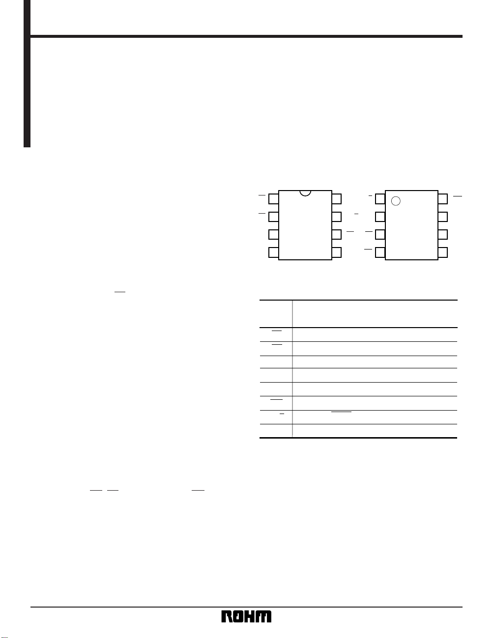
Pin assignments
1
2
3
4
8
7
6
5
CS
SK
DI
DO
V
CC
R / B
∗
WC
GND
BR9010 /
BR9020 / 9040
1
2
3
4
8
7
6
5
R / B
∗
VCC
CS
SK
WC
GND
DO
DI
BR9010F /
BR9010FV /
BR9020F /
BR9040F
•
Pin description
CS
SK
DI
DO
GND
WC
V
CC
R /
B
Function
Chip select input
Serial data clock input
Operating code, address, and serial data input
Serial data output
Reference voltage for all I / O, 0V
Write control input
READY, BUSY status signal output
Power supply connection
Pin
name
∗ This pin is N.C. (non connection) on BR9010.
Page 2
2
Memory ICs
BR9010 / BR9010F / BR9010FV / BR9020 / BR9020F /
BR9040 / BR9040F
•
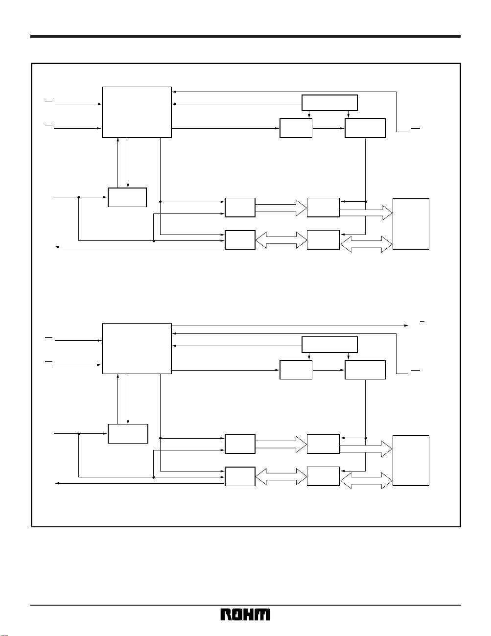
Block diagram
Command decode
Control
Clock generation
High voltage
generator
Write
disable
Address
buffer
Data
register
Command
register
Address
decoder
R / W
amplifier
1024bit
EEPROM
array
16bit
16bit
6bit
CS
SK
DI
DO
WC
6bit
Power supply
voltage detector
7 (8)
bit
2,048
(
4,096) bit
EEPROM
array
16bit
16bit
7 (8)
bit
CS
SK
DI
DO
WC
R / B
∗
Values in parentheses are for the BR9040 / F.
Command decode
Control
Clock generation
Power supply
voltage detector
Write
disable
High voltage
generator
Address
decoder
R / W
amplifier
Address
buffer
Data
register
Command
register
BR9010 / F / FV
BR9020 / F, BR9040 / F
Page 3
3
Memory ICs
BR9010 / BR9010F / BR9010FV / BR9020 / BR9020F /
BR9040 / BR9040F
•
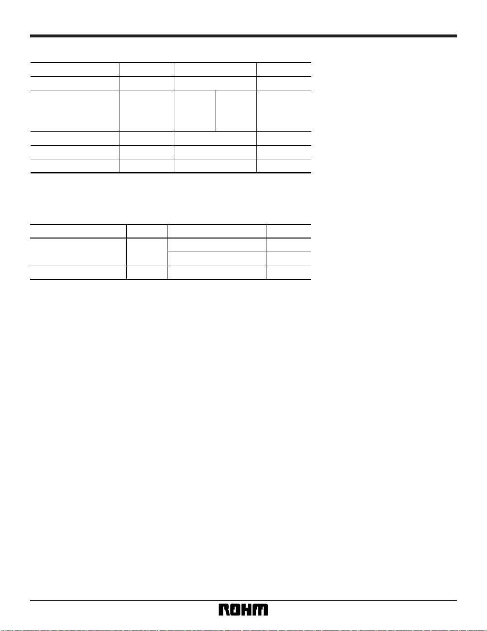
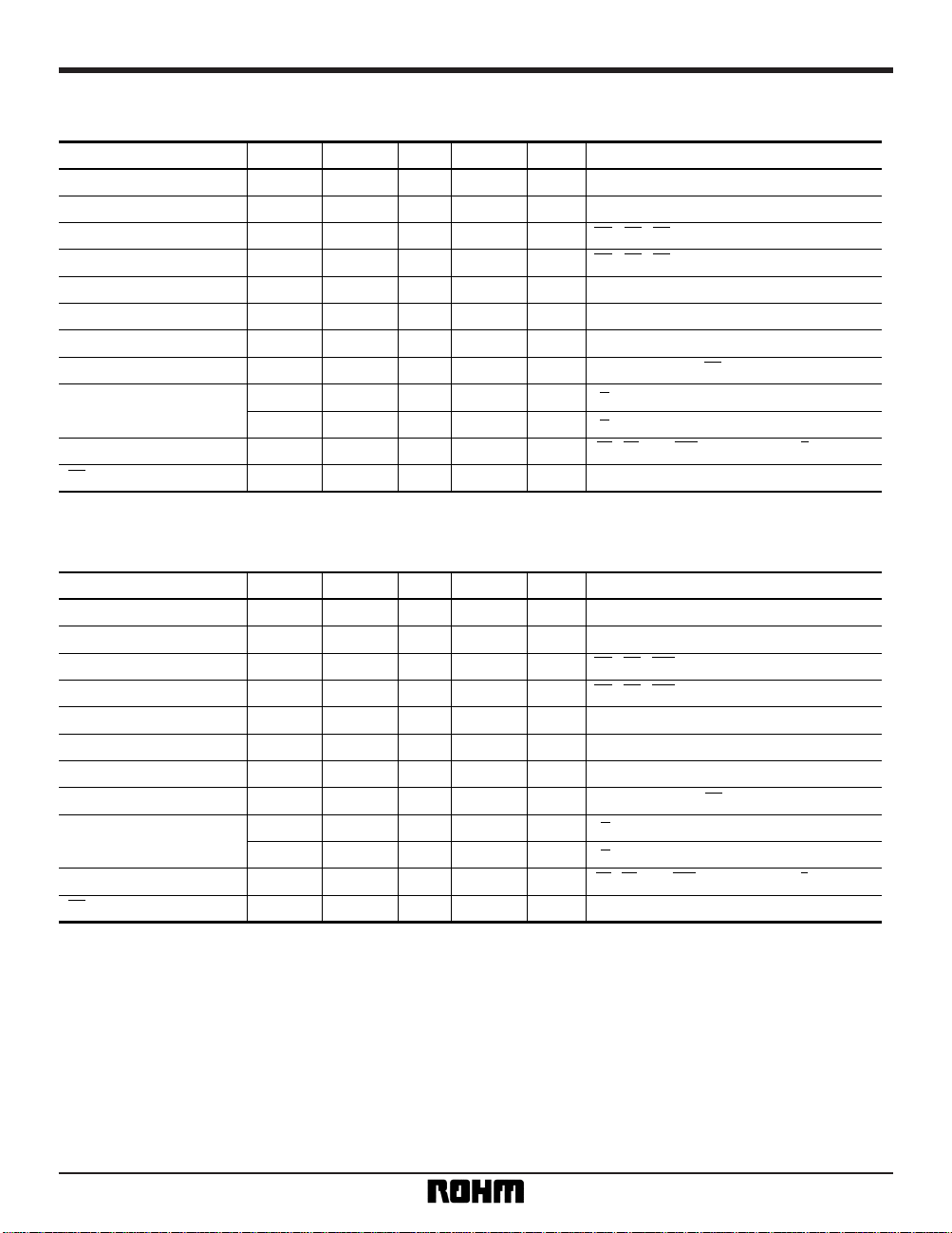
Absolute maximum ratings (Ta = 25°C)
Parameter Symbol Limits Unit
Applied voltage
Power dissipation
Storage temperature
Operation temperature
Input voltage
V
CC
Pd
Tstg
Topr
—
– 0.3 ~ + 7.0
– 65 ~ + 125
– 40 ~ + 85
V
mW
°C
°C
V
∗
Reduced by 5.0mw
∗
1
/ 3.5mw
∗
2
/ 3.0mw
∗
3
for each increase in Ta of 1°C over 25°C.
DIP8
SOP8
SSOP-B8
500
∗
1
350
∗
2
300
∗
3
– 0.3 ~ VCC + 0.3
•
Recommended operating conditions
Parameter Symbol UnitLimits
Power supply voltage
Input voltage
V
CC
VIN
2.7 to 5.5 (write)
2.0 to 5.5 (read)
0 ~ V
CC
V
V
V
Page 4
4
Memory ICs
BR9010 / BR9010F / BR9010FV / BR9020 / BR9020F /
BR9040 / BR9040F
•
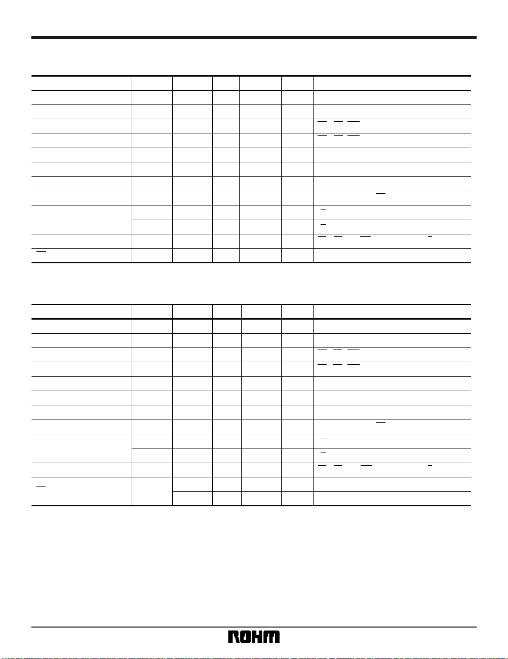
Electrical characteristics
BR9010 / F / FV: At 5V (unless otherwise noted, Ta = – 40 to + 85°C, V
CC = 5V ± 10%)
Parameter
Symbol Min. Typ. Max. Unit Conditions
Input low level voltage 1
Input high level voltage 1
Input low level voltage 2
Input high level voltage 2
Output low level voltage
Output high level voltage
Input leak current
Output leak current
Consumption current
during operation
Standby current
SK frequency
V
IL1
VIH1
VIL2
VIH2
VOL
VOH
ILI
ILO
ICC1
ICC2
ISB
fSK
—
0.7 ×
V
CC
—
0.8 ×
V
CC
0
V
CC –
0.4
—
—
—
—
—
—
—
—
—
—
—
—
—
—
—
—
0.3 ×
V
CC
—
0.2 ×
V
CC
—
0.4
V
CC
1
1
2
1
3
1
V
V
V
V
V
V
µA
µA
mA
mA
µA
MHz
DI Pin
DI Pin
CS, SK, WC Pin
CS, SK, WC Pin
I
OL = 2.1mA
I
OH = – 0.4mA
V
IN = 0V ~ VCC
V
OUT = 0V ~ VCC CS = VCC
f = 1MHz tE / W = 10ms (WRITE)
f = 1MHz (READ)
CS, SK, DI, WC, = V
CC DO = OPEN
– 1
– 1
—
BR9010 / F / FV: At 3V (unless otherwise noted, Ta = – 40 to + 85°C, VCC = 3V ± 10%)
Parameter
Symbol Min. Typ. Max. Unit Conditions
Input low level voltage 1
Input high level voltage 1
Input low level voltage 2
Input high level voltage 2
Output low level voltage
Output high level voltage
Input leak current
Output leak current
Standby current
SK frequency
V
IL1
VIH1
VIL2
VIH2
VOL
VOH
ILI
ILO
ICC1
ICC2
ISB
fSK
—
0.7 ×
V
CC
—
0.8 ×
V
CC
0
V
CC –
0.4
—
—
—
—
—
—
—
—
—
—
—
—
—
—
—
—
0.3 ×
V
CC
—
0.2 ×
V
CC
—
0.4
V
CC
1
1
1.5
500
2
1
V
V
V
V
V
V
µA
µA
mA
µA
µA
MHz
DI Pin
DI Pin
CS, SK, WC Pin
CS, SK, WC Pin
I
OL = 100µA
I
OH = – 100µA
V
IN = 0 ~ VCC
V
OUT = 0 ~ VCC CS = VCC
f = 1MHz tE / W = 15ms (WRITE)
f = 1MHz (READ)
CS, SK, DI, WC, = V
CC DO = OPEN
䊊
Not designed for radiation resistance
–1
–1
—
Consumption current
during operation
Page 5
5
Memory ICs
BR9010 / BR9010F / BR9010FV / BR9020 / BR9020F /
BR9040 / BR9040F
•
Electrical characteristics
•
BR9020 / F: At 5V (unless otherwise noted, Ta = – 40 to + 85°C, VCC = 5V ± 10%)
Parameter
Symbol Min. Typ. Max. Unit Conditions
Input low level voltage 1
Input high level voltage 1
Input low level voltage 2
Input high level voltage 2
Output low level voltage
Output high level voltage
Input leak current
Output leak current
Standby current
SK frequency
V
IL1
VIH1
VIL2
VIH2
VOL
VOH
ILI
ILO
ICC1
ICC2
ISB
fSK
—
0.7 × V
CC
—
0.8 × V
CC
0
V
CC – 0.4
—
—
—
—
—
—
—
—
—
—
—
—
—
—
—
—
0.3 × V
CC
—
0.2 × V
CC
—
0.4
V
CC
1
1
2
1
3
1
V
V
V
V
V
V
µA
µA
mA
mA
µA
MHz
DI Pin
DI Pin
CS, SK, WC Pin
CS, SK, WC Pin
I
OL = 2.1mA
I
OH = – 0.4mA
V
IN = 0V ~ VCC
V
OUT = 0V ~ VCC CS = VCC
fSK = 1MHz tE / W = 10ms (WRITE)
f
SK = 1MHz (READ)
CS, SK, DI, WC, = V
CC DO, R / B = OPEN
—
– 1
– 1
Consumption current
during operation
•
BR9020 / F: At 3V (unless otherwise noted, Ta = – 40 to + 85°C, VCC = 3V ± 10%)
Parameter
Symbol Min. Typ. Max. Unit Conditions
Input low level voltage 1
Input high level voltage 1
Input low level voltage 2
Input high level voltage 2
Output low level voltage
Output high level voltage
Input leak current
Output leak current
Standby current
SK frequency
V
IL1
VIH1
VIL2
VIH2
VOL
VOH
ILI
ILO
ICC1
ICC2
ISB
fSK
—
0.7 × V
CC
—
0.8 × V
CC
0
V
CC – 0.4
—
—
—
—
—
—
—
—
—
—
—
—
—
—
—
—
0.3 × V
CC
—
0.2 × V
CC
—
0.4
V
CC
1
1
1.5
500
2
1
V
V
V
V
V
V
µA
µA
mA
µA
µA
MHz
DI Pin
DI Pin
CS, SK, WC Pin
CS, SK, WC Pin
I
OL = 100µA
I
OH = – 100µA
V
IN = 0V ~ VCC
V
OUT = 0V ~ VCC CS = VCC
fSK = 1MHz tE / W = 15ms (WRITE)
f
SK = 1MHz (READ)
CS, SK, DI, WC, = V
CC DO, R / B = OPEN
—
– 1
– 1
Consumption current
during operation
Page 6
6
Memory ICs
BR9010 / BR9010F / BR9010FV / BR9020 / BR9020F /
BR9040 / BR9040F
•
Electrical characteristics
•
BR9040 / F: At 5V (unless otherwise noted, Ta = – 40 to + 85°C, VCC = 5V ± 10%)
Parameter
Symbol Min. Typ. Max. Unit Conditions
Input low level voltage 1
Input high level voltage 1
Input low level voltage 2
Input high level voltage 2
Output low level voltage
Output high level voltage
Input leak current
Output leak current
Standby current
SK frequency
V
IL1
VIH1
VIL2
VIH2
VOL
VOH
ILI
ILO
ICC1
ICC2
ISB
fSK
—
0.7 × V
CC
—
0.8 × V
CC
0
V
CC – 0.4
—
—
—
—
—
—
—
—
—
—
—
—
—
—
—
—
0.3 × V
CC
—
0.2 × V
CC
—
0.4
V
CC
1
1
2
1
3
1
V
V
V
V
V
V
µA
µA
mA
mA
µA
MHz
DI Pin
DI Pin
CS, SK, WC Pin
CS, SK, WC Pin
I
OL = 2.1mA
I
OH = – 0.4mA
V
IN = 0V ~ VCC
V
OUT = 0V ~ VCC CS = VCC
fSK = 1MHz tE / W = 10ms (WRITE)
f
SK = 1MHz (READ)
CS, SK, DI, WC, = V
CC DO, R / B = OPEN
—
– 1
– 1
Consumption current
during operation
•
BR9040 / F: At 3V (unless otherwise noted, Ta = – 40 to + 85°C, VCC = 3V ± 10%)
Parameter
Symbol Min. Typ. Max. Unit Conditions
Input low level voltage 1
Input high level voltage 1
Input low level voltage 2
Input high level voltage 2
Output low level voltage
Output high level voltage
Input leak current
Output leak current
Standby current
SK frequency
V
IL1
VIH1
VIL2
VIH2
VOL
VOH
ILI
ILO
ICC1
ICC2
ISB
fSK
—
0.7 × V
CC
—
0.8 × V
CC
0
V
CC – 0.4
—
—
—
—
—
—
—
—
—
—
—
—
—
—
—
—
—
—
0.3 × V
CC
—
0.2 × V
CC
—
0.4
V
CC
1
1
1.5
500
2
1
750
V
V
V
V
V
V
µA
µA
mA
µA
µA
MHz
kHz
DI Pin
DI Pin
CS, SK, WC Pin
CS, SK, WC Pin
I
OL = 100µA
I
OH = – 100µA
V
IN = 0V ~ VCC
V
OUT = 0V ~ VCC CS = VCC
fSK = 1MHz tE / W = 15ms (WRITE)
f
SK = 1MHz (READ)
CS, SK, DI, WC, = V
CC DO, R / B = OPEN
V
CC = 3.0 ~ 3.3V
V
CC = 2.7 ~ 3.0V
– 1
– 1
Consumption current
during operation
Page 7

7
Memory ICs
BR9010 / BR9010F / BR9010FV / BR9020 / BR9020F /
BR9040 / BR9040F
•
Operation timing characteristics
BR9010 / F / FV: At 5V (unless otherwise noted, Ta = – 40 to + 85°C, V
CC = 5V ± 10%)
Parameter Symbol UnitMax.Typ.Min.
CS setup time
CS hold time
Data setup time
Data hold time
DO rise delay time
DO fall delay time
Self-timing programming cycle
CS minimum high level time
Time when DO goes High-Z (via CS)
Data clock high level time
Data clock low level time
Write control setup time
Write control hold time
t
CSS
tCSH
tDIS
tDIH
tPD1
tPD0
tE / W
tCS
tOH
tWH
tWL
tWCS
tWCH
200
0
150
150
—
—
—
1
0
450
450
0
0
—
—
—
—
—
—
—
—
—
—
—
—
—
—
—
—
—
350
350
10
—
400
—
—
—
—
ns
ns
ns
ns
ns
ns
ms
µs
ns
ns
ns
ns
ns
•
BR9010 / F / FV: At 3V (unless otherwise noted, Ta = – 40 to + 85°C, VCC = 3V ± 10%)
Parameter Symbol UnitMax.Typ.Min.
CS setup time
CS hold time
Data setup time
Data hold time
DO rise delay time
DO fall delay time
Self-timing programming cycle
CS minimum high level time
Time when DO goes High-Z (via CS)
Data clock high level time
Data clock low level time
Write control setup time
Write control hold time
t
CSS
tCSH
tDIS
tDIH
tPD1
tPD0
tE / W
tCS
tOH
tWH
tWL
tWCS
tWCH
200
0
150
150
—
—
—
1
0
450
450
0
0
—
—
—
—
—
—
—
—
—
—
—
—
—
—
—
—
—
350
350
15
—
400
—
—
—
—
ns
ns
ns
ns
ns
ns
ms
µs
ns
ns
ns
ns
ns
Page 8

8
Memory ICs
BR9010 / BR9010F / BR9010FV / BR9020 / BR9020F /
BR9040 / BR9040F
•
Operation timing characteristics
BR9020 / F / FV: At 5V (unless otherwise noted, Ta = – 40 to + 85°C, V
CC = 5V ± 10%)
Parameter Symbol UnitMax.Typ.Min.
CS setup time
CS hold time
Data setup time
Data hold time
DO rise delay time
DO fall delay time
Self-timing programming cycle
CS minimum high level time
READY / BUSY display valid time
Time when DO goes High-Z (via CS)
Data clock high level time
Data clock low level time
Write control setup time
Write control hold time
t
CSS
tCSH
tDIS
tDIH
tPD1
tPD0
tE / W
tCS
tSV
tOH
tWH
tWL
tWCS
tWCH
200
0
150
150
—
—
—
1
—
0
450
450
0
0
—
—
—
—
—
—
—
—
—
—
—
—
—
—
—
—
—
—
350
350
10
—
1
400
—
—
—
—
ns
ns
ns
ns
ns
ns
ms
µs
µs
ns
ns
ns
ns
ns
•
BR9020 / F / FV: At 3V (unless otherwise noted, Ta = – 40 to + 85°C, VCC = 3V ± 10%)
Parameter Symbol UnitMax.Typ.Min.
CS setup time
CS hold time
Data setup time
Data hold time
DO rise delay time
DO fall delay time
Self-timing programming cycle
CS minimum high level time
READY / BUSY display valid time
Time when DO goes High-Z (via CS)
Data clock high level time
Data clock low level time
Write control setup time
Write control hold time
t
CSS
tCSH
tDIS
tDIH
tPD1
tPD0
tE / W
tCS
tSV
tOH
tWH
tWL
tWCS
tWCH
200
0
150
150
—
—
—
1
—
0
450
450
0
0
—
—
—
—
—
—
—
—
—
—
—
—
—
—
—
—
—
—
350
350
15
—
1
400
—
—
—
—
ns
ns
ns
ns
ns
ns
ms
µs
µs
ns
ns
ns
ns
ns
Page 9

9
Memory ICs
BR9010 / BR9010F / BR9010FV / BR9020 / BR9020F /
BR9040 / BR9040F
•
Operation timing characteristics
BR9040 / F: At 5V (unless otherwise noted, Ta = – 40 to + 85°C, V
CC = 5V ± 10%)
Parameter Symbol UnitMax.Typ.Min.
CS setup time
CS hold time
Data setup time
Data hold time
DO rise delay time
DO fall delay time
Self-timing programming cycle
CS minimum high level time
READY / BUSY display valid time
Time when DO goes High-Z (via CS)
Data clock high level time
Data clock low level time
Write control setup time
Write control hold time
t
CSS
tCSH
tDIS
tDIH
tPD1
tPD0
tE / W
tCS
tSV
tOH
tWH
tWL
tWCS
tWCH
200
0
150
150
—
—
—
1
—
0
500
500
0
0
—
—
—
—
—
—
—
—
—
—
—
—
—
—
—
—
—
—
350
350
10
—
1
400
—
—
—
—
ns
ns
ns
ns
ns
ns
ms
µs
µs
ns
ns
ns
ns
ns
•
BR9040 / F: At 3V (unless otherwise noted, Ta = – 40 to + 85°C, VCC = 3V ± 10%)
Parameter Symbol UnitMax.Typ.Min.
CS setup time
CS hold time
Data setup time
Data hold time
DO rise delay time V
CC
= 3.0 ~ 3.3V
DO fall delay time V
CC
= 3.0 ~ 3.3V
DO rise delay time V
CC
= 2.7 ~ 3.0V
DO fall delay time V
CC
= 2.7 ~ 3.0V
Self-timing programming cycle
CS minimum high level time
READY / BUSY display valid time
Time when DO goes High-Z (via CS)
Data clock high level time V
CC
= 3.0 ~ 3.3V
Data clock low level time V
CC
= 3.0 ~ 3.3V
Data clock high level time V
CC
= 2.7 ~ 3.0V
Data clock low level time V
CC
= 2.7 ~ 3.0V
Write control setup time
Write control hold time
tCSS
tCSH
tDIS
tDIH
tPD1
tPD0
tPD1
tPD0
tE / W
tCS
tSV
tOH
tWH
tWL
tWH
tWL
tWCS
tWCH
200
0
150
150
—
—
—
—
—
1
—
0
500
500
650
650
0
0
—
—
—
—
—
—
—
—
—
—
—
—
—
—
—
—
—
—
—
—
—
—
350
350
500
500
15
—
1
400
—
—
—
—
—
—
ns
ns
ns
ns
ns
ns
ns
ns
ms
µs
µs
ns
ns
ns
ns
ns
ns
ns
Page 10

10
Memory ICs
BR9010 / BR9010F / BR9010FV / BR9020 / BR9020F /
BR9040 / BR9040F
•
Input / output circuits
RESET int. CS int.
CS int.
OE int.
CS
DI
DO
SK
WC
(1) Input circuits
(2) Output circuits
R / B
∗
DO: BR9010 / F / FV
R / B: BR9020 / F, BR9040 / F
OE int.
DO
∗
DO: BR9040 / F
BR9020 / F
•
Circuit operation
(1) Command mode
Command Start bit
1010
1010
1010
1010
Operating code
1000
0100
0011
0000
Address Data
D0 D1—D14 D15
A0 A1 A2 A3 A4 A5 (A6)
夽
2
(A7)
夽
1
A0 A1 A2 A3 A4 A5 (A6)
夽
2
(A7)
夽
1
∗ ∗ ∗ ∗ ∗ ∗ ∗ ∗
∗ ∗ ∗ ∗ ∗ ∗ ∗ ∗
Read
Write
Erase / Write enabled
Erase / Write disable
(READ)
(WRITE)
(EWEN)
(EWDS)
∗
Either V
IH or VIL
With BR9020 / F, 夽1 is ‘0’
With BR9010 / F / FV,
夽1 and 2 are ‘0’
Page 11

tCSS
tCSH
tPD
tDIS
tPD tOH
tDIH
tWH
tCS
tWL
CS
SK
WC
DI
DO
11
Memory ICs
BR9010 / BR9010F / BR9010FV / BR9020 / BR9020F /
BR9040 / BR9040F
(3) Writing enabled / disabled
1) When the power supply is turned on, the latch used to acknowledge writing is reset in the same way as when the
write disable command is executed. Before entering the write mode, the write enabled mode must first be entered.
Once the write enabled mode has been recognized, it remains valid until the write disabled mode is entered, or
the power supply is turned off.
2) The clock is no longer necessary after the first 16 clock pulses have been received. Any subsequent input will be
ignored.
3) WC does not exist for either the write enabled or write disabled command, so WC may be either HIGH or LOW
when the command is being input.
4) Commands are received in these modes by means of 8-bit operating codes. Please be aware that, after an operating code has been entered, commands will not be canceled even if CS is set to HIGH. (To cancel a command,
either turn off the power supply, or input the command once again.)
ENABLE = 1 1
DISABLE = 0 0
H
L
SK
H
L
CS
H
H
Fig.1
L
1
14 8 12 16
0100 0
High-Z
DI
DO
WC H or L
R / B
(2) Timing chart
• Data is read in on the rising edge of SK. Data is output in synchronism with the SK falling edge.
• During a READ operation, data is output from DO in synchronization with the SK rise.
• WC is related to the write command only. Read, erase / write enable, erase / write disable commands can be executed irrespective of the state of WC.
Page 12

12
Memory ICs
BR9010 / BR9010F / BR9010FV / BR9020 / BR9020F /
BR9040 / BR9040F
•
Circuit operation
(4) Read cycle
H
1
1010 000A0 A50 01
4 8 16 32
t
CS
t
OH
STANDBY
L
SK
H
L
CS
H
L
DI
DO
WC H or L
High-Z High-Z
D0 D15
Fig.2 BR9010 / F / FV
H
1
1010 000A0 A601
4 8 16 32
t
CS
tOH
STANDBY
L
SK
H
L
CS
H
L
H
DI
DO
H or L
Fig.3 BR9020 / F
WC
High-Z High-Z
D0 D15
R / B
H
1
1010 000A0 A6A71
4 8 16 32
t
CS
tOH
STANDBY
L
SK
H
L
CS
H
L
H
DI
DO
H or L
Fig.4 BR9040 / F
WC
High-Z High-Z
D0 D15
R / B
1) After the fall of the 16th clock pulse, 16-bit data is output from the DO pin in synchronization with the falling edge of the SK signal.
(DO output changes at a time lag of t
PD0, tPD1 because of internal circuit delay following the falling edge of the SK signal. During the
t
PD0 and tPD1 timing, the tPD time should be assured before data is read, to avoid the previous data being lost. See the synchronized
data input / output timing chart in Fig. 1.)
Page 13

13
Memory ICs
BR9010 / BR9010F / BR9010FV / BR9020 / BR9020F /
BR9040 / BR9040F
•
Circuit operation
(5) Writing cycle
H
L
SK
H
L
CS
H
H
L
L
1
1
48
16 32
0 1 0 0 0 0 A0 A5 0 0 D0
D15
tCS
tE / W
tWCH
1
High-Z High-Z
DI
DO
WC
t
WCS
Fig.5 BR9010 / F / FV
Fig.6 BR9020 / F
H
L
1
101 00 00 0D0
D15
A0 A61
16
32
8
t
CS
tE / W
tSV
4
SK
H
L
CS
H
L
WC
H
DO
H
High-Z High-Z
DI
tWCHtWCS
R / B
Fig.7 BR9040 / F
H
L
1
101 00 00 A7D0
D15
A0 A61
16
32
8
t
CS
tE / W
tSV
4
SK
H
L
CS
H
L
WC
H
DO
H
High-Z High-Z
DI
tWCHtWCS
R / B
Page 14

14
Memory ICs
BR9010 / BR9010F / BR9010FV / BR9020 / BR9020F /
BR9040 / BR9040F
1) During input in the write mode, CS must be LOW, but once writing starts, CS may be either HIGH or LOW.
However, if CS and WC share the same connection, both CS and WC should be set to LOW during writing operations.
(If the WC pin is set to HIGH during a writing operation, writing will be forcibly interrupted at that point. If this happens, the data for that address may be lost, in which case it should be rewritten to that address.)
2) Following input of a write command, CS goes HIGH. If CS is then set to LOW, data will be received from SK and
DI, because the command reception status has been entered.
If CS remains LOW following command input, however, without first going HIGH, command input will be canceled until CS is set to HIGH.
3) Starting from the rising edge of the 32nd clock, the R / B pin goes LOW after RSV has elapsed.
4) The R / B pin is LOW during writing operations. (Following the rising edge of SK after the last data D15 has been
read, the internal timer circuit is activated, and writing of data in the memory cell is automatically completed during t
E / W.) At this point, SK input may be either HIGH or LOW during tE / W.
5) Following input of a write command, if CS falls while SK is LOW, the R / B status can be displayed from the DO
pin. (See the section on READY / BUSY states.)
(6) READY / BUSY display (R / B pin and DO pin)
1) This display outputs the internal status signal; the R / B pin outputs the HIGH or LOW status at all times. The display can also be output from the DO pin. Following completion of the writing command, if CS falls while SK is
LOW, either HIGH or LOW is output. (The display can also be output without using the R / B pin, leaving it open.)
2) When writing data to a memory cell, the READY / BUSY display is output from the rise of the 32nd clock pulse of
the SK signal after t
SV, from the R / B pin.
R / B display = LOW: writing in progress
(The internal timer circuit is activated, and after the t
E / W timing has been created, the timer circuit stops automati-
cally. Writing of data to the memory cell is done during the t
E / W timing, during which time other commands can-
not be received.)
R / B display = HIGH: command standby state
(Writing of data to the memory cell has been completed and the next command can be received.)
CS
DI
DO
READY
Clock
SK
BUSY READY
READY
Write command
HIGH-Z t
PD tOZ
HIGH-Z
BUSY
Fig.8 R / B status output timing
R / B
Page 15

15
Memory ICs
BR9010 / BR9010F / BR9010FV / BR9020 / BR9020F /
BR9040 / BR9040F
•
Operation notes
(1) Turning the power supply on and off
1) When the power supply is turned on and off, CS should be set to HIGH ( = V
CC).
2) When CS is LOW, the command input reception state (active) is entered. If the power supply is turned on in this
state, erroneous operations and erroneous writing can occur because of noise and other factors. To avoid this,
make sure CS is set to HIGH ( = V
CC) before turning on the power supply.
(Good example) Here, the CS pin is pulled up to V
CC.
When turning off the power supply, wait at least 10msec before turning it on again. Failing to
observe this condition can result in the internal circuit failing to be reset when the power supply is turned on.
(Bad example) CS is LOW when the power supply is turned on or off
In this case, because CS remains LOW, the EEPROM may perform erroneous operations or
write erroneous data because of noise or other factors.
∗
Please be aware that the case shown in this example can also occur if CS input is HIGH-Z.
(2) Noise countermeasures
1) SKnoise
If noise occurs at the rise of the SK clock input, the clock is assumed to be excessive, and this can cause malfunction because the bits are out of alignment.
2) WC noise
During a writing operation, noise at the WC pin can be erroneously judged to be data, and this can cause writing
to be forcibly interrupted.
3) V
CC noise
Noise and surges on the power supply line can cause malfunction. We recommend installing a bypass capacitor
between the power supply and ground to eliminate this problem.
VCC
VCC
GND
VCC
GND
Good example Bad example
CS
Page 16

16
Memory ICs
BR9010 / BR9010F / BR9010FV / BR9020 / BR9020F /
BR9040 / BR9040F
(3) Canceling modes
1) Read commands
Cancellation method: CS HIGH
2) Write commands
Canceling methods
a: Canceled by setting CS HIGH. The WC pin is not involved.
b: If the WC pin goes HIGH for even a second, writing is forcibly interrupted. Cancellation occurs even if the CS pin
is HIGH. At this point, data has not been written to the memory, so the data in the designated address has not
yet been changed.
c: The operation is forcibly canceled by setting the WC pin to HIGH or turning off the power supply (although we do
not recommend using this method). The data in the designated address is not guaranteed and should be written
once again.
d: If CS is set to HIGH while the R / B signal is HIGH (following the t
E / W timing), the IC is reset internally, and waits
for the next command to be input.
CS
SK
DI
32 Clock
DO
H or LWC
Cancel can be performed for the entire read mode space
Start bit
4 bits 4 bits 8 bits
16 bits
Operating code Address
DO Data D15
CS
SK
DI
32 clock
WC
Start bit
4 bits 4 bits 8 bits 16 bits
Operating code
Address DO Data D15
R / B
tE / W
a b c d
Page 17

17
Memory ICs
BR9010 / BR9010F / BR9010FV / BR9020 / BR9020F /
BR9040 / BR9040F
•
External dimensions (Units: mm)
DIP8 SSOP-B8
SOP8
0.1
0.22 ± 0.1
0.65
0.3Min.
548
1
6.4 ± 0.3
4.4 ± 0.2
3.0 ± 0.2
1.15 ± 0.1
0.15 ± 0.1
0.1
(0.52)
0.5
±
0.1
3.2
±
0.2 3.4
±
0.3
85
14
9.3
±
0.3
6.5
±
0.3
0.3
±
0.1
0.51Min.
2.54
0°~15°
7.62
0.4 ± 0.11.27
0.15
0.3Min.
0.15 ± 0.1
0.11
6.2 ± 0.3
4.4 ± 0.2
5.0 ± 0.2
85
41
1.5 ± 0.1
 Loading...