

Datasheet BQ4845YS-A4TR, BQ4845YS-A4NTR, BQ4845YS-A4N, BQ4845YS-A4, BQ4845YP-A4 Datasheet (Texas Instruments)
...Page 1
bq4845/bq4845Y
Parallel RTC With CPU Supervisor
Features
➤ Real-Time Clock counts seconds
through years in BCD format
➤ On-chip battery-backup switchover
circuit with nonvolatile control for
external SRAM
➤ Less than 500nA of clock opera-
tion current in backup mode
➤ Microprocessor reset valid to
V
CC=VSS
➤ Independent watchdog timer
with a programmable time-out
period
➤ Power-failinterruptwarning
➤ Programmable clock alarm inter-
rupt active in battery-backup
mode
➤ Programmable periodic interrupt
➤ Battery-low warning
General Description
The bq4845 Real-Time Clock is a
low-power microprocessor peripheral that integrates a time-of-day
clock, a 100-year calendar, and a
CPU supervisor in a 28-pin SOIC or
DIP. The bq4845 is ideal for fax machines, copiers, industrial control
systems, point-of-sale terminals,
data loggers,andcomputers.
The bq4845 provides direct connections for a 32.768KHz quartz crystal
and a 3V backup battery. Through
the use of the conditional chip enable output (CE
voltage output (V
bq4845 can write-protect and make
nonvolatile external SRAMs. The
backup cell powers the real-time
clock and maintains SRAM information in the absence of system
voltage.
The bq4845 contains a temperaturecompensated reference and comparator
circuit that monitors the status of its
voltage supply . When the bq4845 de-
) and battery
OUT
) pins, the
OUT
tects an out-of-tolerance condition, it
generates an interrupt warning and
subsequently a microprocessor reset.
The reset stays active for 200ms after
V
rises within tolerance, to allow for
CC
power supply and processor stabilization.
The bq4845 also has a built-in
watchdog timer to monitor processor
operation. If the microprocessor does
not toggle the watchdog input (WDI)
within the programmed time-out period, the bq4845 asserts WDO
and
RST. WDI unconnected disables the
watchdogtimer.
The bq4845 can generate other interrupts based on a clock alarm condition or a periodic setting. The
alarm interrupt can be set to occur
from once per second to once per
month. The alarm can be made active
in the battery-backup mode to serve
as a system wake-up call. F or interrupts at a rate beyond once per second, the periodic interrupt can be programmed with periods of 30.5µsto
500ms.
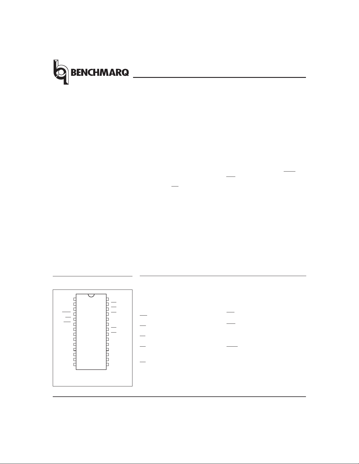
Pin Connections
V
WDO
RST
DQ
Aug.1995
OUT
INT
DQ
DQ
V
X
1
X
2
A
3
A
2
A
1
A
0
0
1
2
SS
1
2
3
4
5
6
7
8
9
10
11
12
13
14
28-DIP or SOIC
28
27
26
25
24
23
22
21
20
19
18
17
16
15
PN484501.eps
V
WE
CE
CE
BC
WDI
OE
CS
V
DQ
DQ
DQ
DQ
DQ
Pin Names
A0–A
CC
IN
OUT
DQ0–DQ7Data inputs/outputs
WE Write enable
OE Output enable
SS
7
8
5
4
3
CS Chip select input
CE
IN
CE
OUT
X1–X2 Crystal inputs
Clock/control address
3
inputs
External RAM chip
enable
Conditional RAM chip
enable
BC Backup battery input
V
OUT
Back-up battery output
INT Interrupt output
RST Microprocessor reset
WDI Watchdoginput
WDO Watchdogoutput
V
CC
V
SS
+5V supply
Ground
1
Page 2
bq4845/bq4845Y
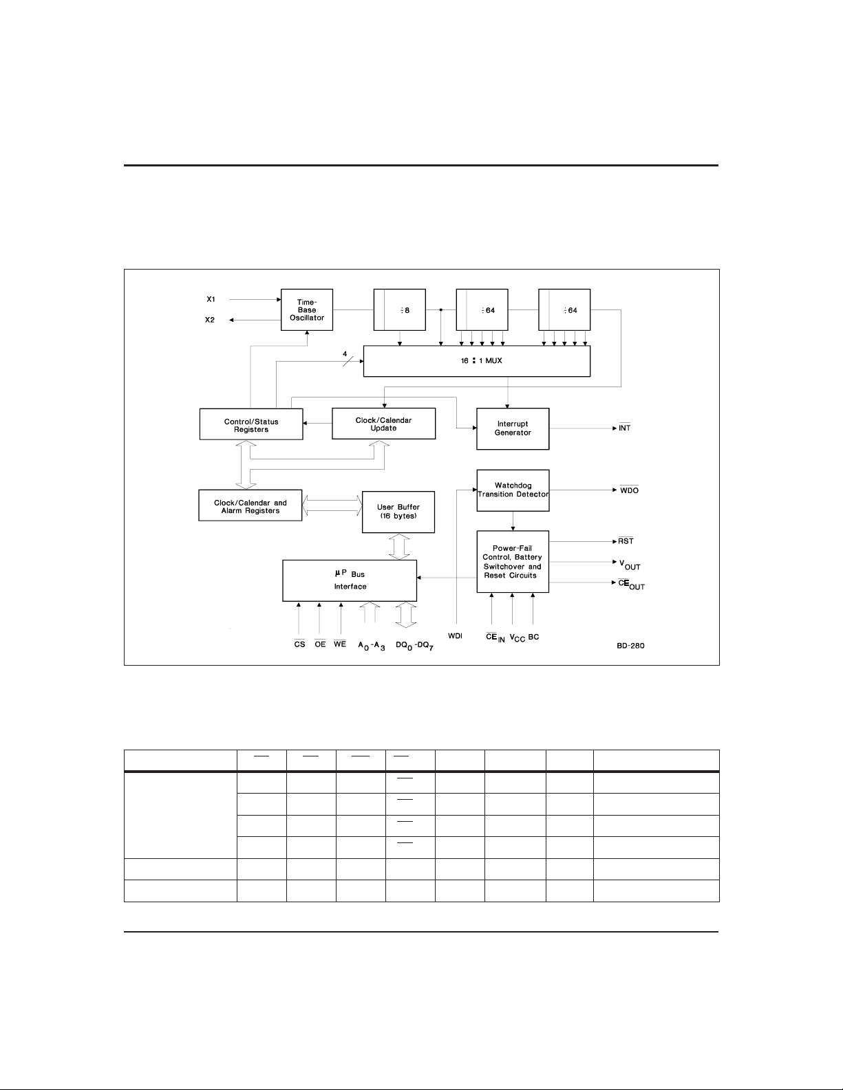
Functional Description
Figure 1 is a block diagram of the bq4845. The following sections describe the bq4845 functional operation
including clock interface, data-retention modes,
power-on reset timing, watchdog timer activation, and
interrupt generation.
Truth Table
V
CC
(max.) V
<V
CC
(min.) V
>V
CC
(min.) > V
<V
PFD
≤ V
SO
Figure 1. Block Diagram
CS OE WE CE
IH
V
IL
IL
V
IL
XXXVOHV
SO
XXXV
XXCEINV
XVILCE
V
V
V
IL
IH
IH
V
IH
V
OUT
V
IN
CE
CE
V
IN
V
IN
OHBVOUT2
2
OUT
OUT1
OUT1
OUT1
OUT1
OUT1
Mode DQ Power
Deselect High Z Standby
Write D
Read D
IN
OUT
Active
Active
Read High Z Active
Deselect High Z CMOS standby
Deselect High Z Battery-backup mode
Aug.1995
Page 3

Pin Descriptions
X1–X2
RST
INT Interrupt output
WDI
WDO
A0–A
Crystal inputs
X1–X2 are a direct connection for a
32.768kHZ, 6pF crystal.
Reset output
RST goes low whenever VCCfalls below the
power fail threshold. RST will remain low for
200ms typical after VCCcrosses the threshold
on power-up. RST also goes low whenever a
watchdog timeout occurs. RST is an opendrain output.
INT goes low when a power fail, periodic, or
alarm condition occurs. INT is an open-drain
output.
Watchdog input
WDI is a three-level input. If WDI remains
either high or low for longer than the
watchdog time-out period (1.5 seconds default), WDO goes low. WDO remains low
until the next transition at WDI. Leaving
WDI unconnected disables the watchdog
function. WDI connects to an internal voltage divider between V
sets it to mid-supply when left unconnected.
Watchdog output
WDO goes low if WDI remains either high
or low longer than the watchdog time-out
period. WDO returns high on the next transition at WDI. WDO remains high if WDI is
unconnected.
Clock address inputs
3
A0–A3allow access to the 16 bytes of realtime clock and control registers.
and VSS, which
OUT
DQ
–DQ7Data input and output
0
DQ0–DQ7provide x8 data for real-time clock
information. These pins connect to the memory data bus.
V
CS
SS
Ground
Chip select
OE Outputenable
OE provides the read control for the RTC
memory locations.
CE
OUT
Chip enable output
CE
goes low only when CEINis low and
OUT
VCCis above the power fail threshold. If
CEINis low, and power fail occurs, CE
stays low for 100µs or until CEINgoes high,
whichever occurs first.
CE
IN
Chip enable input
CEINis the input to the chip-enable gating
circuit.
BC
Backup battery input
BC should be connected to a 3V backup
cell. A voltage within the VBCrange on the
BC pin should be present upon power up to
provide proper oscillator start-up.
V
OUT
Output supply voltage
V
provides the higher of VCCor VBC,
OUT
switched internally, to supply external
RAM.
WE
Write enable
WE provides the write control for the RTC
memory locations.
V
CC
Input supply voltage
+5V input
bq4845/bq4845Y
OUT
Aug.1995
3
Page 4

bq4845/bq4845Y
Address Map
The bq4845 provides 16 bytes of clock and control status
registers. Table 1 is a map of the bq4845 registers, and
Table2describestheregisterbits.
Clock Memory Interface
The bq4845 has the same interface for clock/calendar
and control information as standard SRAM. To read and
write to these locations, the user must put the bq4845 in
the proper mode and meet the timing requirements.
Read Mode
The bq4845 is in read mode whenever OE (Output enable) is low and CS (chip select) is low. The unique address, specified by the 4 address inputs, defines which
one of the 16 clock/calendar bytes is to be accessed. The
bq4845 makes valid data available at the data I/O pins
within tAA(address access time). This occurs after the
last address input signal is stable, and providing the CS
and OE (output enable) access times are met. If the CS
and OE access times are not met, valid data is available
after the latter of chip select access time (t
enable access time (tOE).
and OE control the state of the eight three-state
CS
data I/O signals. If the outputs are activated before tAA,
Table 1. bq4845 Clock and Control Register Map
Ad-
dress
(h) D7 D6 D5 D4 D3 D2 D1 D0
0 0 10-second digit 1-second digit 00–59 Seconds
1 ALM1
2 0 10-minute digit 1-minute digit 00–59 Minutes
3 ALM1
4 PM/AM 0 10-hour digit 1-hour digit 01–12AM/81– 92 PM Hours
ALM1
5
PM/AM
6 0 0 10-day digit 1-day digit 01–31 Day
7 ALM1 ALM0 10-day digit 1-day digit 01–31 Day alarm
8 0 0 0 Day-of-week digit 01–07 Day-of-week
9 0 0 0 10mo. 1-month digit 01–12 Month
A 10-year digit 1-year digit 00–99 Year
B * WD2 WD1 WD0 RS3 RS2 RS1 RS0
C * * AIE PIE PWRIE ABE Interrupt en-
D * * AF PF PWRF BVF Flags
E * * UTI STOP
F * * * * * * * * Unused
Notes: * = Unused bits; unwritable and read as 0.
ALM0
10-second digit
ALM0
10-minute digit
ALM0 10-hour digit 1-hourdigit 01–12AM/ 81–92 PM Hoursalarm
0 = should be set to 0 for valid time/calendar range.
Clock calendar data in BCD. Automatic leap year adjustment.
PM/AM = 1 for PM; PM/AM = 0 for AM.
DSE = 1 enables daylight savings adjustment.
24/12 = 1 enables 24-hour data representation; 24/12 = 0 enables 12-hour data representation.
Day-of-Weekcoded as Sunday = 1 through Saturday = 7.
BVF = 1 for valid battery.
STOP = 1 turns the RTC on; STOP = 0 stops the RTC in back-up mode.
1-second digit 00–59 Seconds alarm
1-minute digit 00–59 Minutes alarm
24/12 DSE Control
12-Hour
Range (h) Register
Programmable
rates
ables
) or output
ACS
Aug.1995
4
Page 5

Table 2. Clock and Control Register Bits
Bits Description
24/12
24- or 12-hour representation
ABE Alarminterrupt enable in
battery-backup mode
AF Alarm interrupt flag
AIE Alarminterrupt enable
ALM0–ALM1 Alarm mask bits
BVF Battery-valid flag
DSE Daylight savings time enable
PF Periodic interrupt flag
PIE Periodic interrupt enable
PM/AM PM or AM indication
PWRF Power-fail interrupt flag
PWRIE Power-failinterrupt enable
RS0–RS3 Periodic interrupt rate
STOP
Oscillator stop and start
UTI Update transfer inhibit
WD0 - WD2 Watchdog time-out rate
the data lines are driven to an indeterminate state until
tAA. If the address inputs are changed while CS and OE
remain low, output data remains valid for tOH(output
data hold time), but goes indeterminate until the next
address access.
Write Mode
The bq4845 is in write mode whenever WE and CS are
active. The start of a write is referenced from the
latter-occurring falling edge of WE or CS. A write is terminated by the earlier rising edge of WE or CS. The addresses must be held valid throughout the cycle. CS or
WE must return high for a minimum of t
t
from WE prior to the initiation of another read or
WR1
write cycle.
Data-in must be valid t
remain valid for t
DH1
prior to the end of write and
DW
or t
afterward. OE should be
DH2
kept high during write cycles to avoid bus contention; although, if the output bus has been activated by a low on
CS and OE, a low on WE disables the outputs tWZafter
WE falls.
WR2
from CS or
bq4845/bq4845Y
Reading the Clock
Once every second, the user-accessible clock/calendar locations are updated simultaneously from the internal
real time counters. To prevent reading data in transition, updates to the bq4845 clock registers should be
halted. Updating is halted by setting the update transfer inhibit (UTI) bit D3 of the control register E. As long
as the UTI bit is 1, updates to user-accessible clock locations are inhibited. Once the frozen clock information is
retrieved by reading the appropriate clock memory locations, the UTI bit should be reset to 0 in order to allow
updates to occur from the internal counters. Because
the internal counters are not halted by setting the UTI
bit, reading the clock locations has no effect on clock accuracy. Once the UTI bit is reset to 0, the internal registers update within one second the user-accessible registers with the correct time. A halt command issued during a clock update allows the update to occur before
freezing the data.
Setting the Clock
The UTI bit must also be used to set the bq4845 clock.
Once set, the locations can be written with the desired
information in BCD format. Resetting the UTI bit to 0
causes the written values to be transferred to the internal clock counters and allows updates to the useraccessible registers to resume within one second.
Stopping and Starting the Clock Oscillator
The bq4845 clock can be programmed to turn off when
the part goes into battery back-up mode by setting
STOP to 0 prior to power down. If the board using the
bq4845 is to spend a significant period of time in storage, the STOP bit can be used to preserve some battery
capacity. STOP set to 1 keeps the clock running when
VCCdrops below VSO. With VCCgreater than VSO, the
bq4845 clockrunsregardlessofthestateofSTOP.
Power-Down/Power-Up Cycle
The bq4845 continuously monitors VCCfor out-oftolerance. During a power failure, when VCCfalls below
V
, the bq4845 write-protects the clock and storage
PFD
registers. When VCCis below VBC(3V typical), the
power source is switched to BC. RTC operation and
storage data are sustained by a valid backup energy
source. When VCCis above VBC, the power source is
VCC. Write-protection continues for t
rises above V
PFD
.
An external CMOS static RAM is battery-backed using
the V
and chip enable output pins from the bq4845.
OUT
As the voltage input VCCslews down during a power
failure, the chip enable output, CE
independent of the chip enable input CE
time after V
CSR
is forced inactive
OUT,
IN.
CC
Aug.1995
5
Page 6
bq4845/bq4845Y
This activity unconditionally write-protects the external
SRAM as VCCfalls below V
. If a memory access is in
PFD
progress to the external SRAM during power-fail detection, that memory cycle continues to completion before
the memory is write-protected. If the memory cycle is
not terminated within time t
, the chip enable output
WPT
is unconditionally driven high, write-protecting the controlled SRAM.
As the supply continues to fall past V
switching device forces V
ergy source. CE
OUT
to the external backup en-
OUT
is held high by the V
, an internal
PFD
OUT
energy
source.
During power-up, V
is switched back to the 5V sup-
OUT
ply as VCCrises above the backup cell input voltage
sourcing V
ter the power supply has reached V
OUT
.CE
is held inactive for time t
OUT
PFD
af-
CER
, independent of
the CEINinput,toallowforprocessorstabilization.
During power-valid operation, the CE
through to the CE
output with a propagation delay of
OUT
input is passed
IN
less than 12ns.
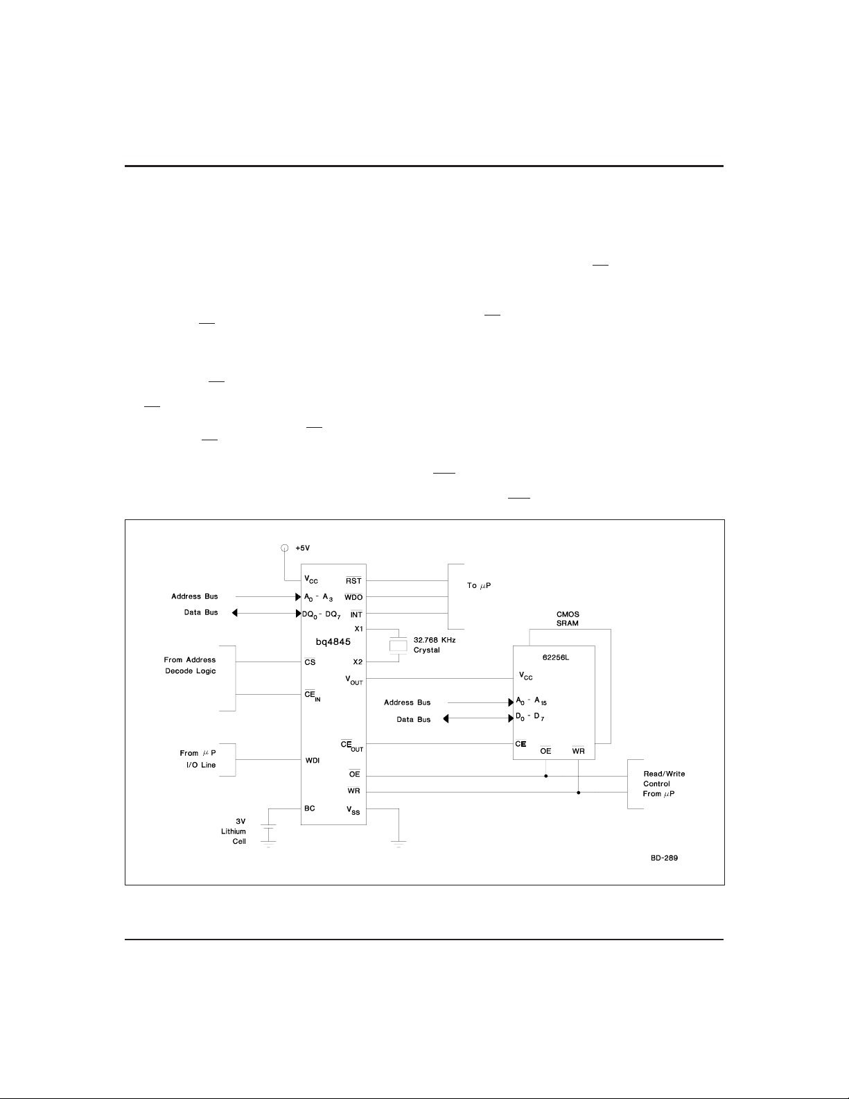
Figure 2 shows the hardware hookup for the external
RAM,battery,and crystal.
A primary backup energy source input is provided on
the bq4845. The BC input accepts a 3V primary battery,
typically some type of lithium chemistry. Since the
bq4845 provides for reverse battery charging protection,
no diode or current limiting resistor is needed in series
with the cell. To prevent battery drain when there is no
valid data to retain, V
OUT
and CE
are internally iso-
OUT
lated from BC by the initial connection of a battery. Following the first application of VCCabove V
, this iso-
PFD
lation is broken, and the backup cell provides power to
V
OUT
and CE
for the external SRAM.
OUT
The crystal should be located as close to X1 and X2 as
possible and meet the specifications in the Crystal
Specification Table. With the specified crystal, the
bq4845 RTC will be accurate to within one minute per
month at room temperature. In the absence of a crystal,
a 32.768 kHz waveform can be fed into X1 with X2
grounded.
Power-On Reset
The bq4845 provides a power-on reset, which pulls the
RST pin low on power-down and remains low on powerup for t
voltage on BC,RST remains valid for VCC=VSS.
after VCCpasses V
RST
With valid battery
PFD.
Figure 2. bq4845 Application Circuit
6
Aug.1995
Page 7

bq4845/bq4845Y
Watchdog Timer
The watchdog monitors microprocessor activity through
the Watchdog input (WDI). To use the watchdog function, connect WDI to a bus line or a microprocessor I/O
line. If WDI remains high or low for longer than the
watchdog time-out period (1.5 seconds default), the
bq4845 asserts WDO and RST.
WatchdogInput
The bq4845 resets the watchdog timer if a change of
state (high to low, low to high, or a minimum 100ns
pulse) occurs at the Watchdog input (WDI) during the
watchdog period. The watchdog time-out is set by WD0WD2 in register B. The bq4845 maintains the watchdog
time-out programming through power cycles. The default state (no valid battery power) of WD0-WD2 is 000
or 1.5s on power-up. Table 3 shows the programmable
watchdog time-out rates. The watchdog time-out period
immediately after a reset is equal to the programmed
watchdogtime-out.
To disable the watchdog function, leave WDI floating. An
internal resistor network (100kΩequivalent impedance
at WDI) biases WDI to approximately 1.6V. Internal
comparators detect this level and disable the watchdog
timer. When V
bq4845 disables the watchdog function and disconnects
WDI from its internal resistor network, thus making it
high impedance.
is below the power-fail threshold, the
CC
WatchdogOutput
The Watchdog output (WDO) remains high if there is a
transition or pulse at WDI during the watchdog timeout period. The bq4845 disables the watchdog function
and WDO is a logic high when VCCis below the power
fail threshold, battery-backup mode is enabled, or WDI
is an open circuit. In watchdog mode, if no transition occurs at WDI during the watchdog time-out period, the
bq4845 asserts RST for the reset time-out period t1.
WDO goes low and remains low until the next transition
at WDI. If WDI is held high or low indefinitely, RST will
generate pulses (t1seconds wide) every t3seconds. Figure 3 shows the watchdogtiming.
Aug.1995
Figure 3. Watchdog Time-out Period and Reset Active Time
7
Page 8

bq4845/bq4845Y
Interrupts
The bq4845 allows three individually selected interrupt
events to generate an interrupt request on the INT pin.
These three interrupt events are:
The periodic interrupt, programmable to occur once
■
every 30.5µs to 500ms
The alarm interrupt, programmable to occur once per
■
second to once per month
The power-fail interrupt, which can be enabled to be
■
asserted when the bq4845 detects a power failure
The periodic, alarm, and power-fail interrupts are enabled by an individual interrupt-enable bit in register C,
the interrupts register. When an event occurs, its event
flag bit in the flags register, register D, is set. If the corresponding event enable bit is also set, then an interrupt
request is generated. Reading the flags register clears
all flag bits and makes INT
the flag register, the bq4845 addresses must be held stable at register D for at least 50ns to avoid inadvertent
resets.
PeriodicInterrupt
Bits RS3–RS0 in the interrupts register program the
rate for the periodic interrupt. The user can interpret
the interrupt in two ways: either by polling the flags
register for PF assertion or by setting PIE so that INT
goes active when the bq4845 sets the periodic flag.
Reading the flags register resets the PF bit and returns
INT to the high-impedance state. Table 4 shows the periodic rates.
Alarm Interrupt
Registers 1, 3, 5, and 7 program the real-time clock
alarm. During each update cycle, the bq4845 compares
the date, hours, minutes, and seconds in the clock regis-
high impedance. To reset
ters with the corresponding alarm registers. If a match
between all the corresponding bytes is found, the alarm
flag AF in the flags register is set. If the alarm interrupt is enabled with AIE, an interrupt request is generated on INT
the flags register. ALM1 – ALM0 in the alarm registers,
mask each alarm compare byte. An alarm byte is
masked by setting ALM1 (D7) and ALM0 (D6) to 1.
Alarm byte masking can be used to select the frequency
of the alarm interrupt,according to Table 5.
The alarm interrupt can be made active while the
bq4845 is in the battery-backup mode by setting ABE in
the interrupts register. Normally, the INT
high-impedance during battery backup. With ABE set,
however, INT is driven low if an alarm condition occurs
and the AIE bit is set. Because the AIE bit is reset during power-on reset, an alarm generated during power-on
reset updates only the flags register. The user can read
the flags register during boot-up to determine if an
alarm wasgeneratedduringpower-onreset.
. The alarm condition is cleared by a read to
pin goes
Power-FailInterrupt
When VCCfalls to the power-fail-detect point, the
power-fail flag PWRF is set. If the power-fail interrupt
enable bit (PWRIE) is also set, then INT is asserted low.
The power-fail interrupt occurs t
generates a reset and deselects. The PWRIE bit is
cleared on power-up.
before the bq4845
WPT
Battery-Low Warning
The bq4845 checks the battery on power-up. When the
battery voltage is approximately 2.1V, the battery-valid
flag BVF in the flags register is set to a 0 indicating that
clockandRAMdatamaybeinvalid.
Table 3. Watchdog Time-out Rates
Normal Watchdog
WD2 WD1 WD0
0 0 0 1.5s 0.25s
0 0 1 23.4375ms 3.9063ms
0 1 0 46.875ms 7.8125ms
0 1 1 93.75ms 15.625ms
1 0 0 187.5ms 31.25ms
1 0 1 375ms 62.5ms
1 1 0 750ms 125ms
1 1 1 3s 0.5s
Time-out Period (t
2,t3
Reset Time-out
)
Period (t1)
8
Aug.1995
Page 9

bq4845/bq4845Y
Table 4. Periodic Interrupt Rates
Register B Bits Periodic Interrupt
RS3 RS2 RS1 RS0 Period Units
0000None
0001 30.5175
0010 61.035
0011 122.070
0100 244.141
0101 488.281
0110 976.5625
0111 1.95315 ms
1000 3.90625 ms
1001 7.8125 ms
1010 15.625 ms
1011 31.25 ms
1100 62.5 ms
1101 125ms
1110 250ms
1111 500ms
s
µ
s
µ
s
µ
s
µ
s
µ
s
µ
Table 5. Alarm Frequency (Alarm Bits D6 and D7 of Alarm Registers)
1h 3h 5h 7h
ALM1•ALM0 ALM1•ALM0 ALM1•ALM0 ALM1•ALM0
1 1 1 1 Once per second
0 1 1 1 Once per minute when seconds match
0 0 1 1 Once per hour when minutes, and seconds match
0 0 0 1 Once per day when hours,minutes,and seconds match
0 0 0 0 When date, hours, minutes, and seconds match
Aug.1995
Alarm Frequency
9
Page 10

bq4845/bq4845Y
Absolute Maximum Ratings
Symbol Parameter Value Unit Conditions
V
CC
V
T
T
OPR
T
STG
T
BIAS
T
SOLDER
DC voltage applied on VCCrelative to V
DC voltage applied on any pin excluding V
relative to V
SS
SS
CC
Operating temperature
Storage temperature -55 to +125 °C
Temperature under bias -40 to +85 °C
Soldering temperature +260 °C For 10 seconds
Note: Permanent device damage may occur if Absolute Maximum Ratings are exceeded. Functional operation
should be limited to the Recommended DC Operating Conditions detailed in this data sheet. Exposure to conditions beyond the operational limits for extended periods of time may affect device reliability.
-0.3 to 7.0 V
-0.3 to 7.0 V V
V
≤
T
CC
0 to +70 °C Commercial
-40 to +85 °C Industrial
+ 0.3
Recommended DC Operating Conditions (T
A=TOPR
)
Symbol Parameter Minimum Typical Maximum Unit Notes
V
CC
Supply voltage
4.5 5.0 5.5 V bq4845Y
4.75 5.0 5.5 V bq4845
V
SS
V
IL
V
IH
V
BC
Supply voltage 0 0 0 V
Input low voltage -0.3 - 0.8 V
Input high voltage 2.2 - VCC+ 0.3 V
Backup cell voltage 2.3 - 4.0 V
Note: Typical values indicate operation at TA= 25°C.
10
Aug.1995
Page 11

bq4845/bq4845Y
DC Electrical Characteristics (T
A=TOPR, VCCmin
V
CC
V
≤
CCmax)
≤
Symbol Parameter Minimum Typical Maximum Unit Conditions/Notes
I
LI
I
LO
V
OH
V
OHB
V
OL
I
CC
I
SB1
I
SB2
V
SO
I
CCB
V
PFD
V
OUT1
V
OUT2
V
RST
V
INT
V
WDO
I
WDIL
I
WDIH
Input leakage current - -
Output leakage current - -
1
±
1
±
AVIN=VSSto V
µ
CS
A
µ
=VIHor OE =VIHor WE
=V
IL
Output high voltage 2.4 - - V IOH= -2.0 mA
V
BC Supply VBC- 0.3 - - V VBC>VCC,IOH= -10µA
OH,
Output low voltage - - 0.4 V IOL= 4.0 mA
Operating supply current - 12 25 mA
Standby supply current - 3 - mA CS =V
Standby supply current - 1.5 - mA
Supply switch-over voltage - V
BC
-V
Battery operation current - 0.3 0.5
Min. cycle, duty = 100%,
CS
=VIL,I
IH
CS
V
≥
CC
0V≤V
IN
or V
≥
IN
V
=3V,TA= 25°C, no load
BC
A
µ
on V
OUT
I/O
- 0.2V,
≤
V
CC
or CE
Power-fail-detectvoltage 4.55 4.62 4.75 V bq4845
Power-fail-detectvoltage 4.30 4.37 4.5 V bq4845Y
V
voltage VCC- 0.3V - - V I
OUT
V
voltage VBC- 0.3V - - V I
OUT
RST output voltage - - 0.4V - I
INT output voltage - - 0.4V - I
WDO output voltage
Watchdoginput low current -50 -10 Watchdoginput high current - 20 50
- - 0.4V - I
2.4 - - - I
A 0<V
µ
A 2.2<V
µ
= 100mA, VCC>V
OUT
= 100µA, VCC<V
OUT
= 4mA
RST
= 4mA
INT
= 4mA
SINK
= 2mA
SOURCE
< 0.8V
WDI
WDI<VCC
CC
= 0mA
0.2V,
- 0.2V
OUT
Notes: Typical values indicate operation at TA= 25°C, VCC=5V.
RST and INT are open-drain outputs.
BC
BC
Crystal Specifications (DT-26 or Equivalent)
Symbol Parameter Minimum Typical Maximum Unit
f
O
C
L
T
P
k Parabolic curvature constant - - -0.042 ppm/°C
Q Quality factor 40,000 70,000 R
1
C
0
C
0/C1
D
L
f/f
∆
O
Aug.1995
Oscillation frequency - 32.768 - kHz
Load capacitance - 6 - pF
Temperature turnover point 20 25 30 °C
Series resistance - - 45 K
Shunt capacitance - 1.1 1.8 pF
Capacitance ratio - 430 600
Drive level - - 1
µ
Aging (first year at 25°C) - 1 - ppm
11
Ω
W
Page 12

bq4845/bq4845Y
Capacitance (T
Symbol Parameter Minimum Typical Maximum Unit Conditions
C
I/O
C
IN
Note: These parameters are sampled and not 100% tested.
Input/output capacitance - - 7 pF Output voltage = 0V
Input capacitance - - 5 pF Input voltage = 0V
= 25°C, F = 1MHz, VCC= 5.0V)
A
AC Test Conditions
Parameter Test Conditions
Input pulse levels 0V to 3.0V
Input rise and fall times 5 ns
Input and output timing reference levels 1.5 V (unless otherwise specified)
Output load (including scope and jig) See Figures 4 and 5
12
Figure 5. Output Load BFigure 4. Output Load A
Aug.1995
Page 13

bq4845/bq4845Y
Read Cycle (T
A=TOPR, VCCmin
V
CC
V
≤
CCmax)
≤
Symbol Parameter Min. Max. Unit Conditions
t
RC
t
AA
t
ACS
t
OE
t
CLZ
t
OLZ
t
CHZ
t
OHZ
t
OH
Write Cycle (T
Read cycle time 70 - ns
Address access time - 70 ns Output load A
Chip select access time - 70 ns Output load A
Output enable to output valid - 35 ns Output load A
Chip select to output in low Z 5 - ns Output load B
Output enable to output in low Z 0 - ns Output load B
Chip deselect to output in high Z 0 25 ns Output load B
Output disable to output in high Z 0 25 ns Output load B
Output hold from address change 10 - ns Output load A
V
A=TOPR , VCCmin
CC
V
≤
≤
CCmax
)
Symbol Parameter Min. Max. Unit Conditions
t
t
t
t
t
t
t
t
t
t
t
t
WC
CW
AW
AS
WP
WR1
WR2
DW
DH1
DH2
WZ
OW
Write cycle time 70 - ns
Chip select to end of write 65 - ns (1)
Address valid to end of write 65 - ns (1)
Address setup time 0 - ns
Write pulse width 55 - ns
Write recovery time (write cycle 1) 5 - ns
Write recovery time (write cycle 2) 15 - ns
Data valid to end of write 30 - ns
Data hold time (write cycle 1) 0 - ns
Data hold time (write cycle 2) 10 - ns
Measured from address valid to beginning
of write. (2)
Measured from beginning of write to end of
write. (1)
Measured from WE
going high to end of
write cycle. (3)
Measured from CS
going high to end of
write cycle. (3)
Measured to first low-to-high transition of
either CS
Measured from WE
or WE.
going high to end of
write cycle. (4)
Measured from CS
going high to end of
write cycle. (4)
Write enabled to output in high Z 0 25 ns I/O pins are in output state. (5)
Output active from end of write 0 - ns I/O pins are in output state. (5)
Notes: 1. A write ends at the earlier transition of CS going high and WE going high.
2. A write occurs during the overlap of a low CS
and a low WE. A write begins at the later transition
of CS going low and WE going low.
or t
or t
must be met.
WR2
must be met.
DH2
3. Either t
4. Either t
5. If CS
WR1
DH1
goes low simultaneously with WE going low or after WE going low,the outputs remain in
high-impedance state.
Aug.1995
13
Page 14

bq4845/bq4845Y
Read Cycle No. 1 (Address Access)
Read Cycle No. 2 (CS Access)
Read Cycle No. 3 (OE Access)
1,3,4
1,5
1,2
Notes: 1. WE is held high for a read cycle.
2. Device is continuously selected: CS
3. Address is valid prior to or coincident with CS
=VIL.
4. OE
5. Device is continuously selected: CS
=OE=VIL.
transition low.
=VIL.
Aug.1995
14
Page 15

bq4845/bq4845Y
Write Cycle No. 1 (WE-Controlled)
Write Cycle No. 2 (CS-Controlled)
1,2,3
1,2,3,4,5
Notes: 1. CS or WE must be high during address transition.
low) during this period, data input signals of opposite polarity to the
Aug.1995
2. Because I/O may be active (OE
outputs must not be applied.
3. If OE
4. Either t
5. Either t
is high, the I/O pins remain in a state of high impedance.
or t
or t
must be met.
WR2
must be met.
DH2
WR1
DH1
15
Page 16

bq4845/bq4845Y
Power-Down/Power-Up Timing (T
A=TOPR
)
Symbol Parameter Minimum Typical Maximum Unit Conditions
t
F
VCCslew from 4.75 to
300 - -
s
µ
4.25V
t
FS
t
R
t
PF
t
WPT
t
CSR
t
RST
VCCslew from 4.25 to V
VCCslew from VSOto
V
PFD(MAX)
Interrupt delay from
V
PFD
Write-protect time for
external RAM
CS at VIHafter power-up 100 200 300 ms
V
to RST inactive t
PFD
10 - -
SO
100 - -
6-24
90 100 125
CSR
-t
CSR
s
µ
s
µ
s
µ
s
µ
Delay after V
V
before SRAM is write-protected
PFD
slews down past
CC
and RST activated.
Internal write-protection period af-
ter V
passes V
CC
on power-up.
PFD
ms Reset active time-out period
Time during which external SRAM
t
t
CER
CED
Chip enable recovery
time
Chip enable propagation
delay to external SRAM
t
CSR
-t
CSR
ms
is write-protected after VCCpasses
V
on power-up.
PFD
- 9 12 ns Output load A
Caution: Negative undershoots below the absolute maximum rating of -0.3V in battery-backup mode
may affect data integrity.
Power-Down/Power-Up Timing
Notes: PWRIE set to “1” to enable power fail interrupt.
RST and INT are open drain and require an external pull-up resistor.
16
Aug.1995
Page 17

28-Pin DIP (P)
bq4845/bq4845Y
28-Pin DIP (P)
Dimension Minimum Maximum
A 0.160 0.190
A1 0.015 0.040
B 0.015 0.022
B1 0.045 0.065
C 0.008 0.013
D 1.440 1.480
E 0.600 0.625
E1 0.530 0.570
e 0.600 0.670
G 0.090 0.110
L 0.115 0.150
S 0.070 0.090
All dimensions are in inches.
Aug.1995
17
Page 18

bq4845/bq4845Y
28-Pin SOIC (S)
28-Pin SOIC (S)
Dimension Minimum Maximum
A 0.095 0.105
A1 0.004 0.012
B 0.013 0.020
C 0.008 0.013
D 0.700 0.715
E 0.290 0.305
e 0.045 0.055
H 0.395 0.415
L 0.020 0.040
All dimensions are in inches.
18
Aug.1995
Page 19

Ordering Information
bq4845 -
bq4845/bq4845Y
TemperatureRange:
Blank = Commercial
N = Industrial
PackageOption:
P = 28-pin plastic DIP (0.600)
S = 28-pin SOIC (0.300)
VoltageTolerance:
Blank = 5%
Y = 10%
Device:
bq4845 Real-Time Clock WithCPUSupervisor
Aug.1995
19
Page 20

IMPORTANT NOTICE
T exas Instruments and its subsidiaries (TI) reserve the right to make changes to their products or to discontinue
any product or service without notice, and advise customers to obtain the latest version of relevant information
to verify, before placing orders, that information being relied on is current and complete. All products are sold
subject to the terms and conditions of sale supplied at the time of order acknowledgement, including those
pertaining to warranty, patent infringement, and limitation of liability.
TI warrants performance of its semiconductor products to the specifications applicable at the time of sale in
accordance with TI’s standard warranty. Testing and other quality control techniques are utilized to the extent
TI deems necessary to support this warranty . Specific testing of all parameters of each device is not necessarily
performed, except those mandated by government requirements.
CERTAIN APPLICATIONS USING SEMICONDUCTOR PRODUCTS MAY INVOLVE POTENTIAL RISKS OF
DEATH, PERSONAL INJURY, OR SEVERE PROPERTY OR ENVIRONMENTAL DAMAGE (“CRITICAL
APPLICATIONS”). TI SEMICONDUCTOR PRODUCTS ARE NOT DESIGNED, AUTHORIZED, OR
WARRANTED TO BE SUITABLE FOR USE IN LIFE-SUPPORT DEVICES OR SYSTEMS OR OTHER
CRITICAL APPLICA TIONS. INCLUSION OF TI PRODUCTS IN SUCH APPLICATIONS IS UNDERST OOD TO
BE FULLY AT THE CUSTOMER’S RISK.
In order to minimize risks associated with the customer’s applications, adequate design and operating
safeguards must be provided by the customer to minimize inherent or procedural hazards.
TI assumes no liability for applications assistance or customer product design. TI does not warrant or represent
that any license, either express or implied, is granted under any patent right, copyright, mask work right, or other
intellectual property right of TI covering or relating to any combination, machine, or process in which such
semiconductor products or services might be or are used. TI’s publication of information regarding any third
party’s products or services does not constitute TI’s approval, warranty or endorsement thereof.
Copyright 1999, Texas Instruments Incorporated
 Loading...