

Datasheet BQ4285LS, BQ4285LP, BQ4285EQ-N, BQ4285EP, BQ4285LSTR Datasheet (Texas Instruments)
Page 1

Features
➤ Direct clock/calendar replace-
ment for IBM
®
AT-compatible
computers and other applications
➤ 114 bytes of general nonvolatile
storage
➤ Enhanced features include:
-
System wake-up capability—
alarm interrupt output active
in battery-backup mode
-
2.7–3.6V operation (bq4285L);
4.5–5.5V operation (bq4285E)
-
32kHz output for power
management
➤ Automatic backup and write-
protect control to external SRAM
➤ Functionally compatible with the
DS1285
➤ Less than 0.5
µ
A load under bat-
tery operation
➤ Selectable Intel or Motorola bus
timing (PLCC), Intel bus timing
(DIP and SOIC)
➤ 14 bytes for clock/calendar and
control
➤ BCD or binary format for clock
and calendar data
➤ Calendar in day of the week, day
of the month, months, and years,
with automatic leap-year adjustment
➤ Time of day in seconds, minutes,
and hours
-
12- or 24-hour format
-
Optional daylight saving
adjustment
➤ Programmable square wave out-
put
➤ Three individually maskable in-
terrupt event flags:
- Periodic rates from 122
µ
s to
500ms
-
Time-of-day alarm once per
second to once per day
- End-of-clock update cycle
➤ 24-pin plastic DIP or SOIC
General Description
The CMOS bq4285E/L is a low-power
microprocessor peripheral providing a
time-of-day clock and 100-year calendar with alarm features and battery
operation. Other features include
three maskable interrupt sources,
square wave output, and 114 bytes of
general nonvolatile storage.
A 32.768kHz output is available for
sustaining power-management activities. Wake-up capability is provided by
an alarm interrupt, which is active in
battery-backup mode.
The bq4285E/L write-protects the
clock, calendar, and storage registers
during power failure. A backup battery then maintains data and operates the clock and calendar.
The bq4285E/L is a fully compatible
real-time clock for IBM ATcompatible computers and other applications. The only external components are a 32.768kHz crystal and a
backup battery.
The bq4285E/L integrates a
battery-backup controller to make a
1
PN428502.eps
28-Pin PLCC
5
6
7
8
9
10
11
25
24
23
22
21
20
19
432
1
282726
12131415161718
AD
0
AD
1
AD
2
AD
3
AD
4
AD
5
NC
AD
6
NC
AD
7
V
SSCSAS
NC
CE
IN
BC
INT
RST
DS
V
SS
R/W
X2X1MOT
V
OUTVCC
SQW
CE
OUT
Pin Names
AD0–AD7Multiplexed address/data
input/output
MOT Bus type select input
(PLCC only )
CS Chip select input
AS Address strobe input
DS Data strobe input
R/W Read/write input
INT Interrupt request output
RST Reset input
SQW Square wave output
BC 3V backup cell input
X1–X2 Crystal inputs
NC No connect
CE
IN
RAM chip enable input
CE
OUT
RAM chip enable output
V
OUT
Supply output
V
CC
+5V supply
bq4285E/L
1
PN428501.eps
24-Pin DIP or SOIC
2
3
4
5
6
7
8
24
23
22
21
20
19
18
17
9
10
16
15
11
12
14
13
V
CC
SQW
CE
OUT
BC
INT
RST
DS
V
SS
R/W
AS
CS
V
OUT
X
1
X
2
AD
0
AD
1
AD
2
AD
3
AD
4
AD
5
AD
6
AD
7
V
SS
CE
IN
Pin Connections
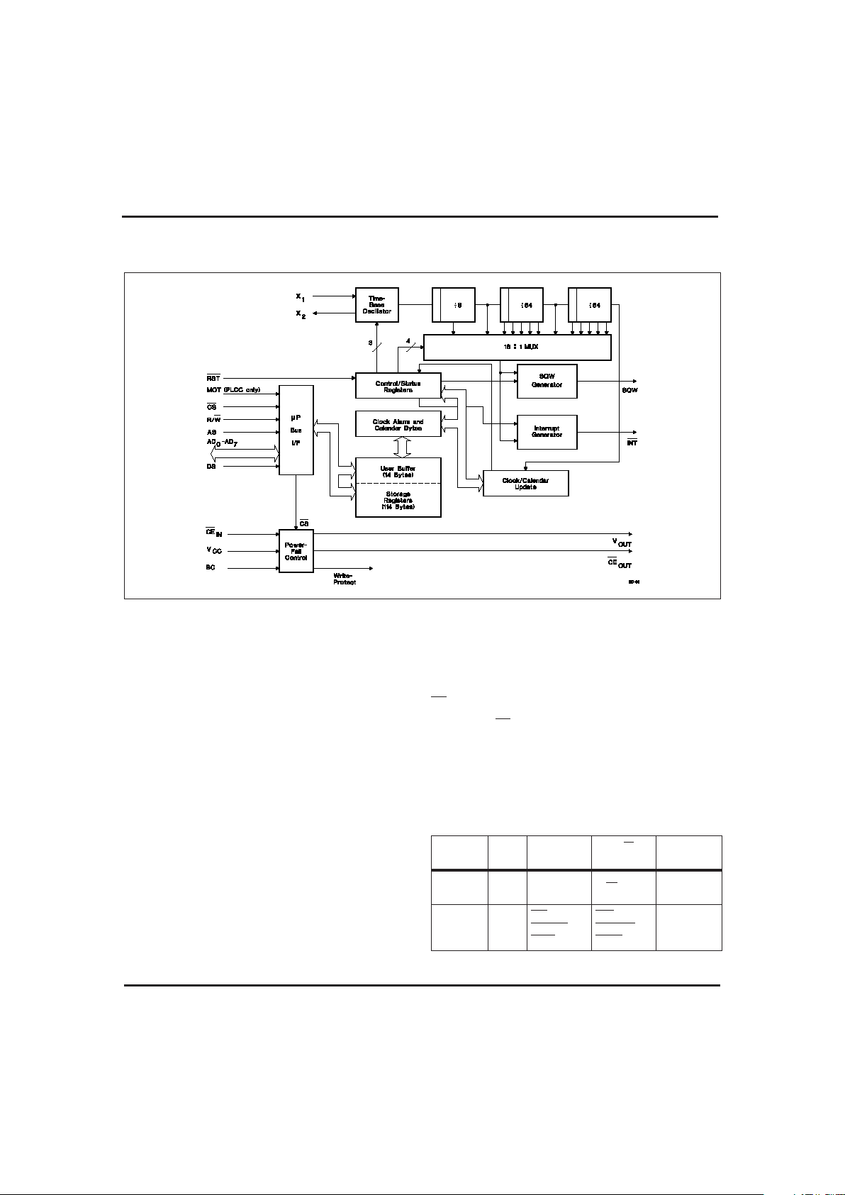
Enhanced RTC With NVRAM Control
Jan.1999 B
Page 2
Block Diagram
standard CMOS SRAM nonvolatile during power-fail
conditions. During power-fail, the bq4285E/L automatically write-protects the external SRAM and provides a VCCoutput sourced from the clock backup
battery.
Pin Descriptions
AD0–AD7Multiplexed address/data input/
output
The bq4285E/L bus cycle consists of two
phases: the address phase and the datatransfer phase. The address phase precedes
the data-transfer phase. During the address phase, an address placed on AD
0
–AD
7
is latched into the bq4285E/L on the falling
edge of the AS signal. During the datatransfer phase of the bus cycle, the AD0–AD
7
pins serve as a bidirectional data bus.
MOT Bus type select input (PLCC package
only)
MOT selects bus timing for either Motorola
or Intel architecture. This pin should be
tied to V
CC
for Motorola timing or to VSSfor
Intel timing (see Table 1).
The setting should not be changed during
system operation. MOT is internally pulled
low by a 20KΩresistor. For the DIP and
SOIC packages, this pin is internally connected to V
SS
, enabling the bus timing for
the Intel architecture.
CS
Chip select input
CS should be driven low and held stable
during the data-transfer phase of a bus cycle accessing the bq4285E/L.
2
Bus
Type
MOT
LevelDSEquivalent
R/W
EquivalentASEquivalent
Motorola
V
CC
DS, E, or
Φ
2
R/W
AS
Intel
V
SS
RD,
MEMR, or
I/OR
WR,
MEMW, or
I/OW
ALE
Table 1. Bus Setup
Jan.1999 B
bq4285E/L
Page 3

AS Address strobe input
AS serves to demultiplex the address/data
bus. The falling edge of AS latches the address on AD0–AD7. This demultiplexing process is independent of the CS signal. For DIP,
SOIC, and PLCC packages with MOT = VCC,
the AS input is provided a signal similar to
ALE in an Intel-based system.
DS Data strobe input
For DIP, SOIC, and PLCC packages with
MOT=V
SS
, the DS input is provided a signal similar to RD, MEMR, or I/OR in an
Intel-based system. The falling edge on DS
is used to enable the outputs during a read
cycle.
For the PLCC package, when MOT = VCC,
DS controls data transfer during a
bq4285E/L bus cycle. During a read cycle,
the bq4285E/L drives the bus after the rising edge on DS. During a write cycle, the
falling edge on DS is used to latch write
data into the chip.
R/W
Read/write input
For DIP, SOIC, and PLCC packages with
MOT=VSS, R/W is provided a signal similar to WR, MEMW, or I/OW in an Intelbased system. The rising edge on R/W
latches data into the bq4285E/L.
For the PLCC package, when MOT = VCC,
the level on R/W identifies the direction of
data transfer. A high level on R/W indicates
a read bus cycle, whereas a low on this pin
indicates a write bus cycle.
INT
Interrupt request output
INT is an open-drain output. This allows
INT to be valid in battery-backup mode for
the alarm interrupt. To use this feature,
INT must be connected to a power supply
other than VCC. INT is asserted low when
any event flag is set and the corresponding
event enable bit is also set. INT becomes
high-impedance whenever register C is read
(see the Control/Status Registers section).
RST
Reset input
The bq4285E/L is reset when RST is pulled
low. When reset, INT becomes highimpedance, and the bq4285E/L is not accessible. Table 4 in the Control/Status Registers
section lists the register bits that are cleared
by a reset.
Reset may be disabled by connecting RST
to
VCC. This allows the control bits to retain their
states through power-down/power-up cycles.
SQW Square-wave output
SQW may output a programmable frequency square-wave signal during normal
(V
CC
valid) system operation. Any one of
the 13 specific frequencies may be selected
through register A. This pin is held low
when the square-wave enable bit (SQWE)
in register B is 0 (see the Control/Status
Registers section).
A 32.768kHz output is enabled by setting
the SQWE bit in register B to 1 and the
32KE bit in register C to 1 after setting
OSC2–OSC0 in register A to 011 (binary).
BC 3V backup cell input
BC should be connected to a 3V backup cell
for RTC operation and storage register nonvolatility in the absence of power. When V
CC
slews down past VBC(3V typical), the integral control circuitry switches the power
source to BC. When VCCreturns above VBC,
the power source is switched to VCC.
Upon power-up, a voltage within the V
BC
range must be present on the BC pin for
the oscillator to start up.
X1–X2 Crystal inputs
The X1–X2 inputs are provided for an external 32.768Khz quartz crystal, Daiwa
DT-26 or equivalent, with 6pF load capacitance. A trimming capacitor may be necessary for extremely precise time-base generation.
CE
IN
External RAM chip enable input,
active low
CE
IN
should be driven low to enable the
controlled external RAM. CEINis internally
pulled up with a 50KΩresistor.
CE
OUT
External RAM chip enable output,
active low
When power is valid, CE
OUT
reflects CE
IN.
V
OUT
Supply output
V
OUT
provides the higher of VCCor VBC,
switched internally, to supply external RAM.
V
CC
Positive power supply
V
SS
Ground
3
Jan.1999 B
bq4285E/L
Page 4
Functional Description
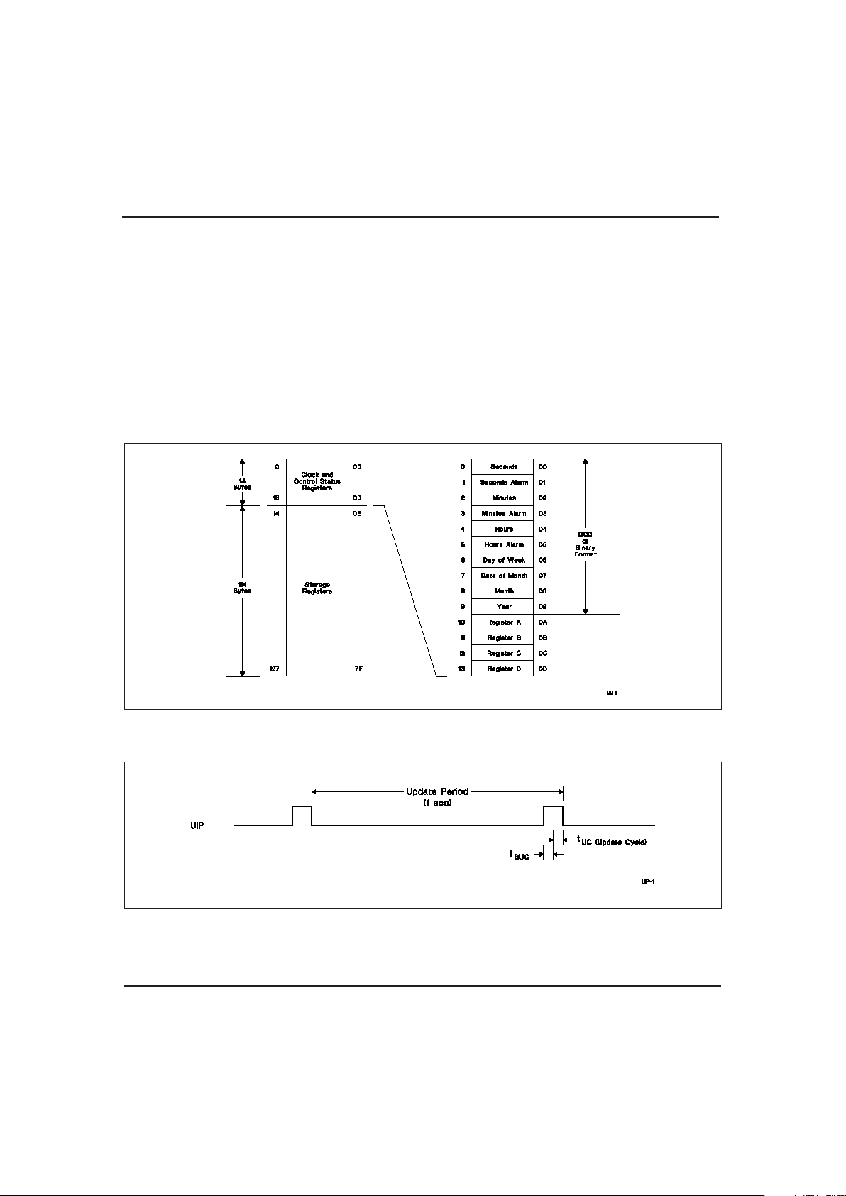
Address Map
The bq4285E/L provides 14 bytes of clock and control/status registers and 114 bytes of general nonvolatile
storage. Figure 1 illustrates the address map for the
bq4285L.
Update Period
The update period for the bq4285E/L is one second. The
bq4285E/L updates the contents of the clock and calendar locations during the update cycle at the end of each
update period (see Figure 2). The alarm flag bit may
also be set during the update cycle.
The bq4285E/L copies the local register updates into the
user buffer accessed by the host processor. Whena1is
written to the update transfer inhibit bit (UTI) in register B, the user copy of the clock and calendar bytes remains unchanged, while the local copy of the same bytes
continues to be updated every second.
The update-in-progress bit (UIP) in register A is set
t
BUC
time before the beginning of an update cycle (see
Figure 2). This bit is cleared and the update-complete
flag (UF) is set at the end of the update cycle.
4
Figure 1. Address Map
Figure 2. Update Period Timing and UIP
Jan.1999 B
bq4285E/L
Page 5

Programming the RTC
The time-of-day, alarm, and calendar bytes can be written
in either the BCD or binary format (see Table 2).
These steps may be followed to program the time, alarm,
and calendar:
1. Modify the contents of register B:
a. Write a 1 to the UTI bit to prevent trans-
fers between RTC bytes and user buffer.
b. Write the appropriate value to the data for-
mat (DF) bit to select BCD or binary format
for all time, alarm, and calendar bytes.
c. Write the appropriate value to the hour
format (HF) bit.
2. Write new values to all the time, alarm, and
calendar locations.
3. Clear the UTI bit to allow update transfers.
On the next update cycle, the RTC updates all 10 bytes
in the selected format.
Square-Wave Output
The bq4285E/L divides the 32.768kHz oscillator frequency to produce the 1 Hz update frequency for the
clock and calendar. Thirteen taps from the frequency divider are fed to a 16:1 multiplexer circuit. The output of
this mux is fed to the SQW output and periodic interrupt generation circuitry. The four least-significant bits
of register A, RS0–RS3, select among the 13 taps (see
Table 3). The square-wave output is enabled by writing
a 1 to the square-wave enable bit (SQWE) in register B.
A 32.768kHz output may be selected by setting
OSC2–OSC0 in register A to 011 while SQWE=1and
32KE = 1.
5
bq4285E/L
Jan.1999 B
Address RTC Bytes
Range
Decimal Binary
Binary-Coded
Decimal
0 Seconds 0–59 00H–3BH 00H–59H
1 Seconds alarm 0–59 00H–3BH 00H–59H
2 Minutes 0–59 00H–3BH 00H–59H
3 Minutes alarm 0–59 00H–3BH 00H–59H
4
Hours, 12-hour format 1–12
01H–OCH AM;
81H–8CH PM
01H–12H AM;
81H–92H PM
Hours, 24-hour format 0–23 00H–17H 00H–23H
5
Hours alarm, 12-hour format 1–12
01H–OCH AM;
81H–8CH PM
01H–12H AM;
81H–92H PM
Hours alarm, 24-hour format 0–23 00H–17H 00H–23H
6 Day of week (1=Sunday) 1–7 01H–07H 01H–07H
7 Day of month 1–31 01H–1FH 01H–31H
8 Month 1–12 01H–0CH 01H–12H
9 Year 0–99 00H–63H 00H–99H
Table 2. Time, Alarm, and Calendar Formats
Page 6

Interrupts
The bq4285E/L allows three individually selected interrupt events to generate an interrupt request. These
three interrupt events are:
n
The periodic interrupt, programmable to occur once
every 122µs to 500 ms.
n
The alarm interrupt, programmable to occur once per
second to once per day, is active in battery-backup
mode, providing a “wake-up” feature.
n
The update-ended interrupt, which occurs at the end
of each update cycle.
Each of the three interrupt events is enabled by an individual interrupt-enable bit in register B. When an event
occurs, its event flag bit in register C is set. If the corresponding event enable bit is also set, then an interrupt
request is generated. The interrupt request flag bit
(INTF) of register C is set with every interrupt request.
Reading register C clears all flag bits, including INTF,
and makes INT
high-impedance.
Two methods can be used to process bq4285E/L interrupt events:
n
Enable interrupt events and use the interrupt request
output to invoke an interrupt service routine.
n
Do not enable the interrupts and use a polling routine
to periodically check the status of the flag bits.
The individual interrupt sources are described in detail
in the following sections.
PeriodicInterrupt
The mux output used to drive the SQW output also
drives the interrupt-generation circuitry. If the periodic
interrupt event is enabled by writinga1totheperiodic
interrupt enable bit (PIE) in register C, an interrupt request is generated once every 122µs to 500ms. The period between interrupts is selected by the same bits in
register A that select the square wave frequency (see Table 3). Setting OSC2–OSC0 in register A to 011 does
not affect the periodic interrupt timing.
6
Jan.1999 B
Register A Bits Square Wave Periodic Interrupt
OSC2 OSC1 OSC0 RS3 RS2 RS1 RS0 Frequency Units Period Units
0100000 None None
0100001256 Hz 3.90625 ms
0100010128 Hz 7.8125 ms
0100011 8.192 kHz 122.070
µ
s
0100100 4.096 kHz 244.141
µ
s
0100101 2.048 kHz 488.281
µ
s
0100110 1.024 kHz 976.5625
µ
s
0100111512 Hz 1.95315 ms
0101000256 Hz 3.90625 ms
0101001128 Hz 7.8125 ms
010101064 Hz 15.625 ms
010101132 Hz 31.25 ms
010110016 Hz 62.5 ms
0101101 8 Hz 125 ms
0101110 4 Hz 250 ms
0101111 2 Hz 500 ms
0 1 1XXXX
32.768
kHz
same as above defined
by RS3–RS0
Table 3. Square-Wave Frequency/Periodic Interrupt Rate
bq4285E/L
Page 7
Alarm Interrupt
The alarm interrupt request is valid in battery-backup
mode, providing a “wake-up” capability. During each update cycle, the RTC compares the hours, minutes, and
seconds bytes with the three corresponding alarm bytes.
If a match of all bytes is found, the alarm interrupt
event flag bit, AF in register C, is set to 1. If the alarm
event is enabled,an interrupt request is generated.
An alarm byte may be removed from the comparison by
setting it to a “don’t care” state. An alarm byte is set to a
“don’t care” state by writinga1toeachofitstwomostsignificant bits. A “don’t care” state may be used to select
the frequency of alarm interrupt events as follows:
n
If none of the three alarm bytes is “don’t care,” the
frequency is once per day, when hours, minutes, and
seconds match.
n
If only the hour alarm byte is “don’t care,” the
frequency is once per hour, when minutes and
seconds match.
n
If only the hour and minute alarm bytes are “don’t care,”
the frequency is once per minute, when seconds match.
n If the hour, minute, and second alarm bytes are
“don’t care,” the frequency is once per second.
Update CycleInterrupt
The update cycle ended flag bit (UF) in register C is set to
a 1 at the end of an update cycle. If the update interrupt
enable bit (UIE) of register B is 1, and the update transfer
inhibit bit (UTI) in register B is 0, then an interrupt request is generated at the end of each update cycle.
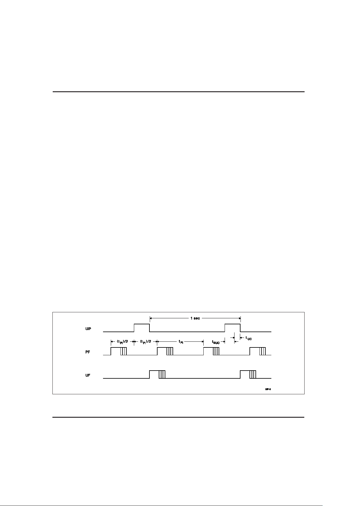
Accessing RTC bytes
Time and calendar bytes read during an update cycle
may be in error. Three methods to access the time and
calendar bytes without ambiguity are:
n
Enable the update interrupt event to generate
interrupt requests at the end of the update cycle.
The interrupt handler has a maximum of 999ms to
access the clock bytes before the next update cycle
begins (see Figure 3).
n
Poll the update-in-progress bit (UIP) in register A. If
UIP = 0, the polling routine has a minimum of t
BUC
time to access the clock bytes (see Figure 3).
n
Use the periodic interrupt event to generate
interrupt requests every tPItime, such that UIP = 1
always occurs between the periodic interrupts. The
interrupt handler will have a minimum of tPI/2 +
t
BUC
time to access the clock bytes (see Figure 3).
Oscillator Control
When power is first applied to the bq4285E/L and VCCis
above V
PFD
, the internal oscillator and frequency divider
are turned on by writing a 010 pattern to bits 4 through 6
of register A. A pattern of 011 behaves as 010 but additionally transforms register C into a read/write register.
This allows the 32.768kHz output on the square wave pin
to be turned on. A pattern of 11X turns the oscillator on,
but keeps the frequency divider disabled. Any other pattern to these bits keeps the oscillator off.
7
bq4285E/L
Figure 3. Update-Ended/Periodic Interrupt Relationship
Jan.1999 B
Page 8
Power-Down/Power-Up Cycle
The bq4285E/L power-up/power-down cycles are different. The bq4285L continuously monitors VCCfor out-oftolerance. During a power failure, when VCCfalls below
V
PFD
(2.53V typical), the bq4285L write-protects the clock
and storage registers. The power source is switched to BC
when VCCis less than V
PFD
and BC is greater than V
PFD
,
or when VCCis less than VBCand VBCis less than V
PFD
.
RTC operation and storage data are sustained by a valid
backup energy source. When VCCis above V
PFD
, the power
source is VCC. Write-protection continues for t
CSR
time af-
ter VCCrises above V
PFD
.
The bq4285E continuously monitors V
CC
for out-oftolerance. During a power failure, when VCCfalls below
V
PFD
(4.17V typical), the bq4285E write-protects the clock
and storage registers. When VCCis below VBC(3V typical),
the power source is switched to BC. RTC operation and
storage data are sustained by a valid backup energy source.
When VCCis above VBC, the power source is VCC. Writeprotection continues for t
CSR
time after VCCrises above
V
PFD
.
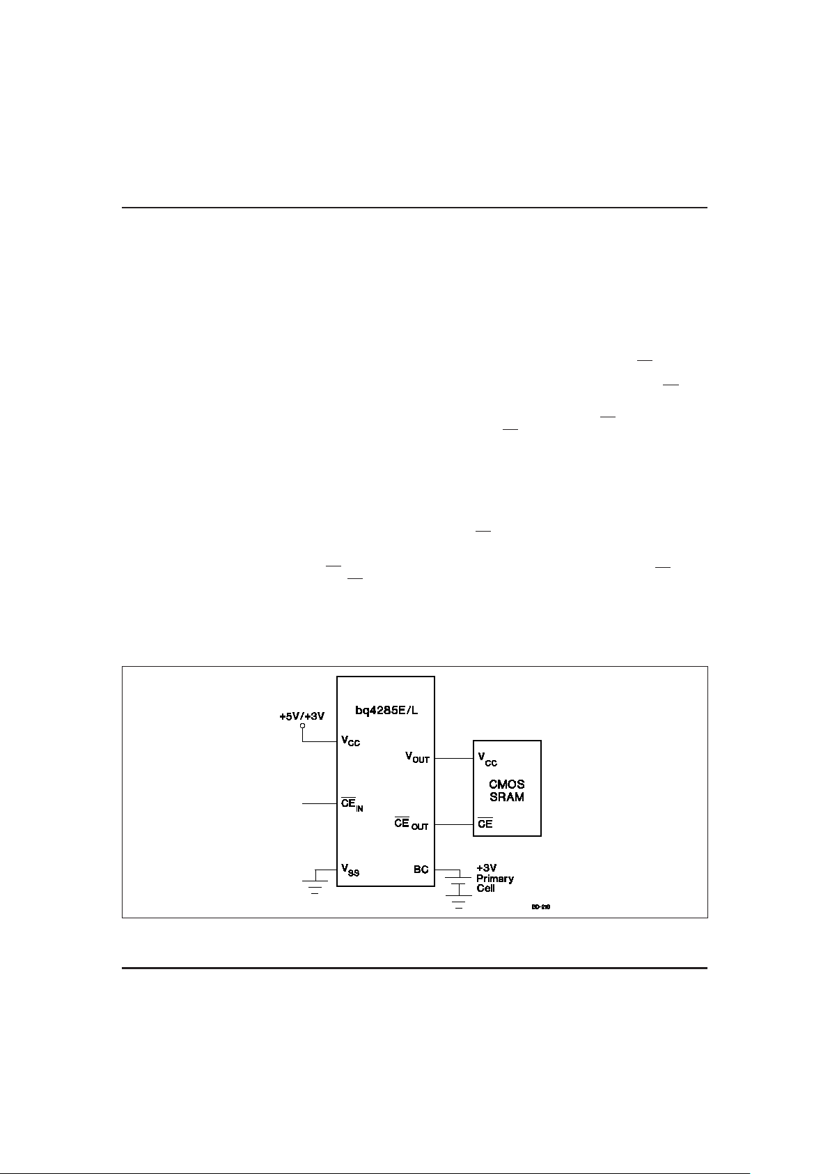
An external CMOS static RAM is battery-backed using
the V
OUT
and chip enable output pins from the
bq4285E/L. As the voltage input VCCslows down during
a power failure, the chip enable output, CE
OUT,
is forced
inactive independent of the chip enable input CE
IN.
This activity unconditionally write-protects the external
SRAM as VCCfalls below V
PFD
. If a memory access is in
process to the external SRAM during power-fail detection, that memory cycle continues to completion before
the memory is write-protected. If the memory cycle is
not terminated within time t
WPT
(30µs maximum), the
chip enable output is unconditionally driven high,
write-protecting the controlled SRAM.
As the supply continues to fall past V
PFD
, an internal
switching device forces V
OUT
to the external backup energy
source. CE
OUT
is held high by the V
OUT
energy source.
During power-up, V
OUT
is switched back to the main
supply as VCCrises above the backup cell input voltage
sourcing V
OUT
.IfV
PFD<VBC
on the bq4285L, the
switch to the main supply occurs at V
PFD
.CE
OUT
is held
inactive for time t
CER
(200ms maximum) after the power
supply has reached V
PFD
, independent of the CEINin-
put, to allow for processor stabilization.
During power-valid operation, the CE
IN
input is passed
through to the CE
OUT
output with a propagation delay
of less than 10ns.
Figure 4 shows the hardware hookup for the external RAM.
A primary backup energy source input is provided on
the bq4285E/L. The BC input accepts a 3V primary battery, typically some type of lithium chemistry. To prevent battery drain when there is no valid data to retain,
V
OUT
and CE
OUT
are internally isolated from BC by the
initial connection of a battery. Following the first application of VCCabove V
PFD
, this isolation is broken, and
the backup cell provides power to V
OUT
and CE
OUT
for
the external SRAM.
8
bq4285E/L
Jan.1999 B
Figure 4. External RAM Hookup to the bq4285E/L RTC
Page 9

Control/Status Registers
The four control/status registers of the bq4285E/L are
accessible regardless of the status of the update cycle
(see Table 4).
Register A
Register A programs:
n
The frequency of the square-wave and the periodic
event rate.
n
Oscillator operation.
Register A provides:
n
Status of the update cycle.
RS0–RS3 - FrequencySelect
These bits select one of the 13 frequencies for the SQW output and the periodic interrupt rate, as shown in Table 3.
OS0–OS2 - OscillatorControl
These three bits control the state of the oscillator and divider stages. A pattern of 010 enables RTC operation by
turning on the oscillator and enabling the frequency di-
vider. A pattern of 011 behaves as 010 but additionally
transforms register C into a read/write register. This allows the 32.768kHz output on the square wave pin to be
turned on. A pattern of 11X turns the oscillator on, but
keeps the frequency divider disabled. When 010 is written, the RTC begins its first update after 500ms.
UIP - UpdateCycle Status
This read-only bit is set prior to the update cycle. When
UIP equals 1, an RTC update cycle may be in progress.
UIP is cleared at the end of each update cycle. This bit
is also cleared when the update transfer inhibit (UTI)
bit in register B is 1.
Register B
Register B enables:
n Update cycle transfer operation
n Square-wave output
n
Interrupt events
n
Daylight saving adjustment
Register B selects:
n
Clock and calendar data formats
All bits of register B are read/write.
9
bq4285E/L
Jan.1999 B
76543210
----RS3RS2RS1RS0
76543210
-OS2OS1OS0----
Register A Bits
76543210
UIP OS2 OS1 OS0 RS3 RS2 RS1 RS0
76543210
UIP-------
Register B Bits
7654 3 210
UTI PIE AIE UIE SQWE DF HF DSE
Reg.
Loc.
(Hex) Read Write
Bit Name and State on Reset
7 (MSB) 6 5 4 3 2 1 0 (LSB)
A 0A Yes Yes
1
UIP na OS2 na OS1 na OS0 na RS3 na RS2 na RS1 na RS0 na
B 0B Yes Yes UTI na PIE 0 AIE 0 UIE 0 SQWE 0 DF na HF na DSE na
C 0C Yes No
2
INTF 0 PF 0 AF 0 UF 0 - 0 32KE na - 0 - 0
D 0DYesNoVRTna-0-0-0 - 0-0-0-0
Notes: na = not affected.
1. Except bit 7.
2. Read/write only when OSC2–OSC0 in register A is 011 (binary).
Table 4. Control/Status Registers
Page 10

DSE - DaylightSaving Enable
This bit enables daylight-saving time adjustments when
written to 1:
n
On the last Sunday in October, the first time the
bq4285E/L increments past 1:59:59 AM, the time
falls back to 1:00:00 AM.
n
On the first Sunday in April, the time springs
forward from 2:00:00 AM to 3:00:00 AM.
HF - HourFormat
This bit selects the time-of-day and alarm hour format:
1 = 24-hour format
0 = 12-hour format
DF - DataFormat
This bit selects the numeric format in which the time,
alarm, and calendar bytes are represented:
1 = Binary
0 = BCD
SQWE - Square-Wave Enable
This bit enables the square-wave output:
1 = Enabled
0 = Disabled and held low
UIE - UpdateCycle InterruptEnable
This bit enables an interrupt request due to an update
ended interrupt event:
1 = Enabled
0 = Disabled
The UIE bit is automatically cleared when the UTI bit
equals 1.
AIE - AlarmInterrupt Enable
This bit enables an interrupt request due to an alarm
interrupt event:
1 = Enabled
0 = Disabled
PIE - Periodic Interrupt Enable
This bit enables an interrupt request due to a periodic
interrupt event:
1 = Enabled
0 = Disabled
UTI - UpdateTransfer Inhibit
This bit inhibits the transfer of RTC bytes to the user
buffer:
1 = Inhibits transfer and clears UIE
0 = Allows transfer
10
Jan.1999 B
7654 3 210
---- - -HF-
7654 3 210
---- - --DSE
7654 3 210
---- -DF--
7654 3 210
----SQWE - - -
7654 3 210
---UIE- ---
7654 3 210
--AIE- - ---
7654 3 210
UTI--- - ---
7654 3 210
-PIE-- - ---
bq4285E/L
Page 11

Register C
Register C is the read-only event status register.
Bits 0–3 -Unused Bits
These bits are always set to 0.
32KE–32KHz Enable Output
This bit may be set to a 1 only when the OSC2–OSC0
bits in register A are set to 011. Setting OSC2–OSC0 to
anything other than 011 clears this bit. If SQWE in register B and 32KE are set, a 32.768KHz waveform is output on the square wave pin.
UF - Update-EventFlag
This bit is set toa1attheendoftheupdate cycle.
Reading register C clears this bit.
AF - AlarmEvent Flag
This bit is set to a 1 when an alarm event occurs. Reading register C clears this bit.
PF - Periodic Event Flag
This bit is set to a 1 every t
PI
time, where tPIis the time
period selected by the settings of RS0–RS3 in register A.
Reading register C clears this bit.
INTF - InterruptRequest Flag
This flag is set to a 1 when any of the following is true:
AIE = 1 and AF = 1
PIE = 1 and PF = 1
UIE = 1 and UF = 1
Reading register C clears this bit.
Register D
Register D is the read-only data integrity status register.
Bits 0–6 -Unused Bits
These bits are always set to 0.
VRT - Valid RAM andTime
1 = Valid backup energy source
0 = Backup energy source is depleted
When the backup energy source is depleted (VRT = 0),
data integrity of the RTC and storage registers is not
guaranteed.
11
Jan.1999 B
7654 3 210
---UF- ---
7654 3 210
--AF- - ---
7654 3 210
-PF- - - - - -
7654 3 210
INTF - - - - - - -
Register D Bits
7654 3 210
VRT000 0 000
7654 3 210
-000 0 000
7654 3 210
VRT--- - ---
Register C Bits
7654 3 210
INTF PF AF UF 0 32KE 0 0
7654 3 210
---- 0 -00
7654 3 210
---- -32KE - -
bq4285E/L
Page 12

12
Jan.1999 B
Absolute Maximum Ratings—bq4285L
Symbol Parameter Value Unit Conditions
V
CC
DC voltage applied on VCCrelative to V
SS
-0.3 to 6.0 V
V
T
DC voltage applied on any pin excluding V
CC
relative to V
SS
-0.3 to 6.0 V
V
T
≤
V
CC
+ 0.3
T
OPR
Operating temperature 0 to +70 °C Commercial
T
STG
Storage temperature -55 to +125 °C
T
BIAS
Temperature under bias -40 to +85 °C
T
SOLDER
Soldering temperature 260 °C For 10 seconds
Note: Permanent device damage may occur if Absolute Maximum Ratings are exceeded.
Functional operation should be limited to the Recommended DC Operating Conditions detailed
in this data sheet. Exposure to conditions beyond the operational limits for extended periods of
time may affect device reliability.
Absolute Maximum Ratings—bq4285E
Symbol Parameter Value Unit Conditions
V
CC
DC voltage applied on VCCrelative to V
SS
-0.3 to 7.0 V
V
T
DC voltage applied on any pin excluding V
CC
relative to V
SS
-0.3 to 7.0 V
V
T
≤
V
CC
+ 0.3
T
OPR
Operating temperature
0 to +70 °C Commercial
-40 to +85 °C Industrial “N”
T
STG
Storage temperature -55 to +125 °C
T
BIAS
Temperature under bias -40 to +85 °C
T
SOLDER
Soldering temperature 260 °C For 10 seconds
Note: Permanent device damage may occur if Absolute Maximum Ratings are exceeded. Functional operation
should be limited to the Recommended DC Operating Conditions detailed in this data sheet. Exposure to
conditions beyond the operational limits for extended periods of time may affect device reliability.
bq4285E/L
Page 13

13
Jan.1999 B
Recommended DC Operating Conditions—bq4285L (T
A
= T
OPR
)
Symbol Parameter Minimum Typical Maximum Unit
V
CC
Supply voltage 2.7 3.15 3.6 V
V
IL
Input low voltage -0.3 - 0.6 V
V
IH
Input high voltage 2.2 - VCC+ 0.3 V
V
BC
Backup cell voltage 2.4 - 4.0 V
Notes: Typical values indicate operation at TA= 25°C.
Potentials are relative to VSS.
Recommended DC Operating Conditions—bq4285E (T
A
= T
OPR
)
Symbol Parameter Minimum Typical Maximum Unit
V
CC
Supply voltage 4.5 5.0 5.5 V
V
IL
Input low voltage -0.3 - 0.8 V
V
IH
Input high voltage 2.2 - VCC+ 0.3 V
V
BC
Backup cell voltage 2.5 - 4.0 V
Notes: Typical values indicate operation at TA= 25°C.
Potentials are relative to VSS.
Crystal Specifications—bq4285E/L (DT-26 or Equivalent)
Symbol Parameter Minimum Typical Maximum Unit
f
O
Oscillation frequency - 32.768 - kHz
C
L
Load capacitance - 6 - pF
T
P
Temperature turnover point 20 25 30 °C
k Parabolic curvature constant - - -0.042 ppm/°C
Q Quality factor 40,000 70,000 -
R
1
Series resistance - - 45 K
Ω
C
0
Shunt capacitance - 1.1 1.8 pF
C
0/C1
Capacitance ratio - 430 600
D
L
Drive level - - 1
µ
W
∆
f/f
O
Aging (first year at 25°C) - 1 - ppm
bq4285E/L
Page 14

14
Jan.1999 B
DC Electrical Characteristics—bq4285E (T
A
= T
OPR
, VCC= 5V±10%)
Symbol Parameter Minimum Typical Maximum Unit Conditions/Notes
I
LI
Input leakage current - -
±
1
µ
AVIN= VSSto V
CC
I
LO
Output leakage current - -
±
1
µ
A
AD
0
–AD7, INT, and SQW
in high impedance,
V
OUT
= VSSto V
CC
V
OH
Output high voltage 2.4 - - V IOH= -2.0 mA
V
OL
Output low voltage - - 0.4 V IOL= 4.0 mA
I
CC
Operating supply current - 7 15 mA
Min. cycle, duty = 100%,
I
OH
= 0mA, IOL= 0mA
V
SO
Supply switch-over voltage - V
BC
-V
I
CCB
Battery operation current - 0.3 0.5
µ
A
V
BC
= 3V, TA= 25°C, no
load on V
OUT
or CE
OUT
I
CCSB
Standby supply current - 300 -
µ
A
VIN= VCCor VSS,
CS≥VCC- 0.2,
no load on V
OUT
V
PFD
Power-fail-detect voltage 4.0 4.17 4.35 V
V
OUT1
V
OUT
voltage VCC- 0.3V - - V I
OUT
= 100mA, VCC>V
BC
V
OUT2
V
OUT
voltage VBC- 0.3V I
OUT
= 100µA, VCC< V
BC
I
MOTH
Input current when MOT = V
CC
- - -275
µ
A Internal 20K pull-down
I
CE
Chip enable input current - - 100
µ
A Internal 50K pull-up
Note: Typical values indicate operation at TA= 25°C, VCC= 5V or VBC= 3V.
bq4285E/L
Page 15

15
Jan.1999 B
DC Electrical Characteristics—bq4285L (T
A
= T
OPR
, VCC= 3.13V±0.45%)
Symbol Parameter Minimum Typical Maximum Unit Conditions/Notes
I
LI
Input leakage current - -
±
1
µ
AVIN= VSSto V
CC
I
LO
Output leakage current - -
±
1
µ
A
AD
0
–AD7, INT, and SQW
in high impedance,
V
OUT
= VSSto V
CC
V
OH
Output high voltage 2.2 - - V IOH= -2.0 mA
V
OL
Output low voltage - - 0.4 V IOL= 4.0 mA
I
CC
Operating supply current - 5 9 mA
Min. cycle, duty = 100%,
I
OH
= 0mA, IOL= 0mA
V
SO
Supply switch-over voltage
-V
PFD
-VV
BC
> V
PFD
-VBC-VV
BC
< V
PFD
I
CCB
Battery operation current - 0.3 0.5
µ
A
V
BC
= 3V, TA= 25°C, no
load on V
OUT
or CE
OUT
I
CCSB
Standby supply current - 100 -
µ
A
VIN= VCCor VSS,
CS
≥
V
CC
- 0.2,
no load on V
OUT
V
PFD
Power-fail-detect voltage 2.4 2.53 2.65 V
V
OUT1
V
OUT
voltage VCC- 0.3V - - V I
OUT
= 80mA, VCC>V
BC
V
OUT2
V
OUT
voltage VBC- 0.3V I
OUT
= 100µA, VCC< V
BC
I
MOTH
Input current when MOT = V
CC
- - -185
µ
A Internal 30K pull-down
I
CE
Chip enable input current - - 120
µ
A Internal 30K pull-up
Note: Typical values indicate operation at TA= 25°C, VCC= 3V.
bq4285E/L
Page 16

16
Jan.1999 B
Capacitance—bq4285E/L (T
A
= 25°C, F = 1MHz, VCC= 5.0V)
Symbol Parameter Minimum Typical Maximum Unit Conditions
C
I/O
Input/output capacitance - - 7 pF V
OUT
= 0V
C
IN
Input capacitance - - 5 pF VIN= 0V
Note: This parameter is sampled and not 100% tested. It does not include the X1 or X2 pin.
except INT
For all outputs
OL-10
510
50pF
+5V
960
Figure 5. Output Load A—bq4285E
INT
OL-11
130pF
+5V
1.15K
Figure 6. Output Load B—bq4285E
AC Test Conditions—bq4285E
Parameter Test Conditions
Input pulse levels 0 to 3.0 V
Input rise and fall times 5 ns
Input and output timing reference levels 1.5 V (unless otherwise specified)
Output load (including scope and jig) See Figures 5 and 6
bq4285E/L
Page 17

17
Jan.1999 B
AC Test Conditions—bq4285L
Parameter Test Conditions
Input pulse levels 0 to 2.3 V
Input rise and fall times 5 ns
Input and output timing reference levels 1.2 V (unless otherwise specified)
Output load (including scope and jig) See Figures 7 and 8
Figure 7. Output Load A—bq4285L Figure 8. Output Load B—bq4285L
bq4285E/L
Page 18

18
Jan.1999 B
Read/Write Timing—bq4285E (T
A
= T
OPR
, VCC= 5V±10%)
Symbol Parameter Minimum Typical Maximum Unit Notes
t
CYC
Cycle time 160 - - ns
t
DSL
DS low or RD/WR high time 80 - - ns
t
DSH
DS high or RD/WR low time 55 - - ns
t
RWH
R/W hold time 0 - - ns
t
RWS
R/W setup time 10 - - ns
t
CS
Chip select setup time 5 - - ns
t
CH
Chip select hold time 0 - - ns
t
DHR
Read data hold time 0 - 25 ns
t
DHW
Write data hold time 0 - - ns
t
AS
Address setup time 20 - - ns
t
AH
Address hold time 5 - - ns
t
DAS
Delay time, DS to AS rise 10 - - ns
t
ASW
Pulse width, AS high 30 - - ns
t
ASD
Delay time, AS to DS rise
(RD/WR fall)
35 - - ns
t
OD
Output data delay time from DS
rise (RD fall)
- - 50 ns
t
DW
Write data setup time 30 - - ns
t
BUC
Delay time before update - 244 -
µ
s
t
PI
Periodic interrupt time interval ----See Table 3
t
UC
Time of update cycle - 1 -
µ
s
bq4285E/L
Page 19

19
Jan.1999 B
Read/Write Timing—bq4285L (T
A
= T
OPR
, VCC= 3.15V±0.45%)
Symbol Parameter Minimum Typical Maximum Unit Notes
t
CYC
Cycle time 270 - - ns
t
DSL
DS low or RD/WR high time 135 - - ns
t
DSH
DS high or RD/WR low time 90 - - ns
t
RWH
R/W hold time 0 - - ns
t
RWS
R/W setup time 15 - - ns
t
CS
Chip select setup time 8 - - ns
t
CH
Chip select hold time 0 - - ns
t
DHR
Read data hold time 0 - 40 ns
t
DHW
Write data hold time 0 - - ns
t
AS
Address setup time 30 - - ns
t
AH
Address hold time 15 - - ns
t
DAS
Delay time, DS to AS rise 15 - - ns
t
ASW
Pulse width, AS high 50 - - ns
t
ASD
Delay time, AS to DS rise
(RD/WR fall)
55 - - ns
t
OD
Output data delay time from DS
rise (RD fall)
- - 100 ns
t
DW
Write data setup time 50 - - ns
t
BUC
Delay time before update - 244 -
µ
s
t
PI
Periodic interrupt time interval ----See Table 3
t
UC
Time of update cycle - 1 -
µ
s
bq4285E/L
Page 20

20
Jan.1999 B
Motorola Bus Read/Write Timing—bq4285E/L (PLCC Package Only)
bq4285E/L
Page 21

21
Intel Bus Write Timing—bq4285E/L
bq4285E/L
Intel Bus Read Timing—bq4285E/L
Jan.1999 B
Page 22

22
Jan.1999 B
Power-Down/Power-Up Timing—bq4285E (T
A
= T
OPR
)
Symbol Parameter Minimum Typical Maximum Unit Conditions
t
F
VCCslew from 4.5V to 0V 300 - -
µ
s
t
R
VCCslew from 0V to 4.5V 100 - -
µ
s
t
CSR
CS at VIHafter power-up
20 - 200 ms
Internal write-protection
period after V
CC
passes V
PFD
on power-up.
t
WPT
Write-protect time for
external RAM
10 16 30
µ
s
Delay after V
CC
slows down
past V
PFD
before SRAM is
write-protected.
t
CER
Chip enable recovery time
t
CSR
-
t
CSR
ms
Time during which external
SRAM is write-protected after
VCCpasses V
PFD
on power-up.
t
CED
Chip enable propagation
delay to external SRAM
- 7 10 ns
Caution: Negative undershoots below the absolute maximum rating of -0.3V in battery-backup mode
may affect data integrity.
Power-Down/Power-Up Timing—bq4285E
bq4285E/L
Page 23

23
Jan.1999 B
Power-Down/Power-Up Timing—bq4285L (T
A
= T
OPR
)
Symbol Parameter Minimum Typical Maximum Unit Conditions
t
F
VCCslew from 2.7V to 0V 300 - -
µ
s
t
R
VCCslew from 0V to 2.7V 100 - -
µ
s
t
CSR
CS at VIHafter power-up
20 - 200 ms
Internal write-protection
period after V
CC
passes V
PFD
on power-up.
t
WPT
Write-protect time for external RAM
-0 - V
BC
> V
PFD
10 16 30
µ
sVBC< V
PFD
t
CER
Chip enable recovery time
t
CSR
-
t
CSR
ms
Time during which external
SRAM is write-protected after
VCCpasses V
PFD
on power-up.
t
CED
Chip enable propagation
delay to external SRAM
- 9 15 ns
Caution: Negative undershoots below the absolute maximum rating of -0.3V in battery-backup mode
may affect data integrity.
Power-Down/Power-Up Timing—bq4285L
bq4285E/L
Page 24

24
Jan.1999 B
Interrupt Delay Timing—bq4285E/L (PLCC Package Only)
Interrupt Delay Timing—bq4285E/L
(TA= T
OPR
)
Symbol Parameter Minimum Typical Maximum Unit
t
RSW
Reset pulse width 5 - -
µ
s
t
IRR
INT release from RST --2
µ
s
t
IRD
INT release from DS (RD)--2
µ
s
Interrupt Delay Timing—bq4285E/L (SOIC, DIP Packages)
bq4285E/L
Page 25

25
Jan.1999 B
bq4285E/bq4285L
P: 24-Pin DIP(0.600"
)
24-Pin P(0.600" DIP
)
Dimension
Inches Millimeters
Min. Max. Min. Max.
A 0.160 0.190 4.06 4.83
A1 0.015 0.040 0.38 1.02
B 0.015 0.022 0.38 0.56
B1 0.045 0.065 1.14 1.65
C 0.008 0.013 0.20 0.33
D 1.240 1.280 31.50 32.51
E 0.600 0.625 15.24 15.88
E1 0.530 0.570 13.46 14.48
e 0.600 0.670 15.24 17.02
G 0.090 0.110 2.29 2.79
L 0.115 0.150 2.92 3.81
S 0.070 0.090 1.78 2.29
e
B
.004
L
D
E
H
C
A1
A
S: 24-Pin SOIC(0.300"
)
24-Pin S(0.300" SOIC
)
Dimension
Inches Millimeters
Min. Max. Min. Max.
A 0.095 0.105 2.41 2.67
A1 0.004 0.012 0.10 0.30
B 0.013 0.020 0.33 0.51
C 0.008 0.013 0.20 0.33
D 0.600 0.615 15.24 15.62
E 0.290 0.305 7.37 7.75
e 0.045 0.055 1.14 1.40
H 0.395 0.415 10.03 10.54
L 0.020 0.040 0.51 1.02
Page 26

26
Jan.1999 B
bq4285E/bq4285L
Q: 28-Pin Quad PLCC
28-Pin Q(Quad PLCC
)
Dimension
Inches Millimeters
Min. Max. Min. Max.
A 0.165 0.180 4.19 4.57
A1 0.020 - 0.51 -
B 0.012 0.021 0.30 0.53
B1 0.025 0.033 0.64 0.84
C 0.008 0.012 0.20 0.30
D 0.485 0.495 12.32 12.57
D1 0.445 0.455 11.30 11.56
D2 0.390 0.430 9.91 10.92
E 0.485 0.495 12.32 12.57
E1 0.445 0.455 11.30 11.56
E2 0.390 0.430 9.91 10.92
e 0.045 0.055 1.14 1.40
Page 27

27
Jan.1999 B
bq4285E/bq4285L
Ordering Information
bq4285E/L -
Package Option:
P = 24-pin plastic DIP (0.600)
S = 24-pin SOIC (0.300)
Q = 28-pin quad PLCC—Last time buy
Device:
bq4285E Real-Time Clock With NVRAM Control
or
bq4285L Real-Time Clock With NVRAM Control
Temperature:
blank = Commercial (0 to +70°C)
N = Industrial* (-40 to +85°C)
*Contact factory for availability.
Data Sheet Revision History
Change No. Page No. Description Nature of Change
1 1, 25 Package option change Last time buy for PLCC
Notes: Change 1 = Jan. 1999 B changes from May 1994.
Page 28

IMPORTANT NOTICE
T exas Instruments and its subsidiaries (TI) reserve the right to make changes to their products or to discontinue
any product or service without notice, and advise customers to obtain the latest version of relevant information
to verify, before placing orders, that information being relied on is current and complete. All products are sold
subject to the terms and conditions of sale supplied at the time of order acknowledgement, including those
pertaining to warranty, patent infringement, and limitation of liability.
TI warrants performance of its semiconductor products to the specifications applicable at the time of sale in
accordance with TI’s standard warranty. Testing and other quality control techniques are utilized to the extent
TI deems necessary to support this warranty. Specific testing of all parameters of each device is not necessarily
performed, except those mandated by government requirements.
CERT AIN APPLICATIONS USING SEMICONDUCTOR PRODUCTS MAY INVOLVE POTENTIAL RISKS OF
DEATH, PERSONAL INJURY, OR SEVERE PROPERTY OR ENVIRONMENTAL DAMAGE (“CRITICAL
APPLICATIONS”). TI SEMICONDUCTOR PRODUCTS ARE NOT DESIGNED, AUTHORIZED, OR
WARRANTED TO BE SUITABLE FOR USE IN LIFE-SUPPORT DEVICES OR SYSTEMS OR OTHER
CRITICAL APPLICATIONS. INCLUSION OF TI PRODUCTS IN SUCH APPLICA TIONS IS UNDERSTOOD T O
BE FULLY AT THE CUSTOMER’S RISK.
In order to minimize risks associated with the customer’s applications, adequate design and operating
safeguards must be provided by the customer to minimize inherent or procedural hazards.
TI assumes no liability for applications assistance or customer product design. TI does not warrant or represent
that any license, either express or implied, is granted under any patent right, copyright, mask work right, or other
intellectual property right of TI covering or relating to any combination, machine, or process in which such
semiconductor products or services might be or are used. TI’s publication of information regarding any third
party’s products or services does not constitute TI’s approval, warranty or endorsement thereof.
Copyright 1999, Texas Instruments Incorporated
 Loading...