

Datasheet BQ4014YMB-85, BQ4014YMB-120, BQ4014MB-85, BQ4014MB-120 Datasheet (Texas Instruments)
Page 1
bq4014/bq401 4Y
256Kx8 Nonvolatile SRAM
Features
➤ Data retention in the absence of
power
➤ Automatic write-protection
during power-up/power-down
cycles
➤ Industry-standard 32-pin 256K x
8 pinout
➤ Conventional SRAM operation;
unlimited write cycles
➤ 10-year minimum data retention
in absence of power
➤ Battery internally isolate d until
power is applied
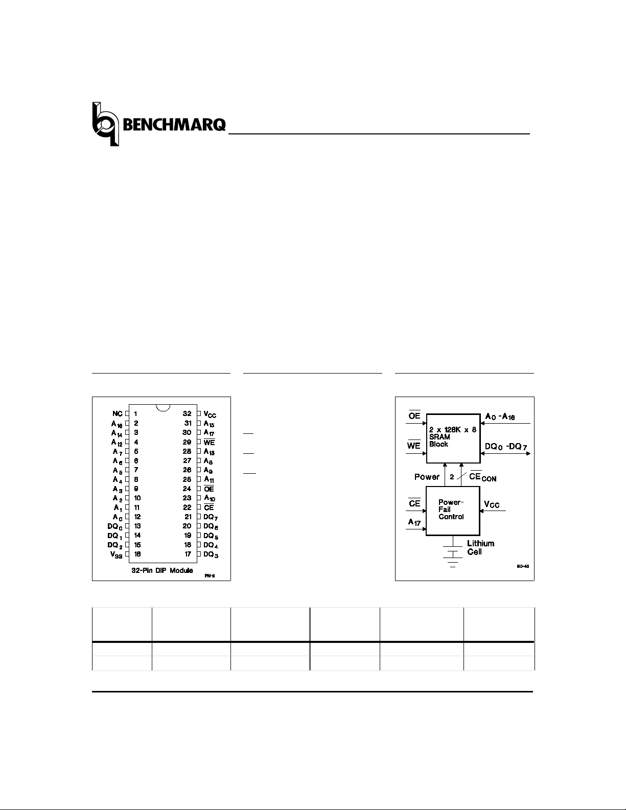
Pin Connections
General Descrip ti on
The CMOS bq4014 is a nonvolatile
2,097,152-bit static RAM organized as
262,144 words by 8 bits. The integral
control circuitry and lithium energy
source provide reliable nonvolatility
coupled with the unlimited write
cycles of standard SRAM.
The control circuitry constantly
monitors the single 5V supply for an
out-of-tolerance condition. When
V
falls out of tolerance, the SRAM
CC
is unconditionally write-protected to
prevent inadvertent write operation.
At this time the integral energy
Pin Names
A0–A
DQ
0
CE Chip enable input
OE Output enable input
WE Write enable input
Address inputs
17
–DQ7Data input/output
source is switched on to sustain the
memory until after V
valid.
The bq4014 uses extremely low
standby current CMOS SRAMs,
coupled with small lithium coin
cells to pro vid e n o nv ol at il it y w i th out
long w rit e-cy cl e tim es an d th e wri tecycle limitations associated with
EEPROM.
The bq4014 requires no external circuitry and is compatible with the
industry-standard 2Mb SRAM
pinout.
returns
CC
Block Diagram
Selection Guide
Part
Number
bq4014 -85
bq4014 -120
Sept. 1992
Maximum
Access
Time (ns)
NC No connect
V
CC
V
SS
Negative
Supply
Tolerance
85 -5%
120 -5%
+5 volt supply input
Ground
Part
Number
bq4014Y -85
bq4014Y -120
1
Maximum
Access
Time ( ns)
85 -10%
120 -10%
Negative
Supply
Tolerance
Page 2
bq4014/bq4014Y
Functional Description
When power is valid, the bq4014 operates as a standard
CMOS SRAM. During power-down and power-up cycles,
the bq4 014 ac ts as a no nvolati le memo ry, automa tically
protecting and preserving the memory contents.
Power-down/power-up control circuitry constantly
monit ors t he V
. The bq4014 monitors for V
V
PFD
use in sy stems wi th 5% sup ply tolera nce. The bq4014 Y
monitors f or V
10% supply tolerance.
When V
CC
automatically write-protects the data. All outputs
become high impedance, and all inputs are treated as
“don’t care.” If a valid access is in process at the time of
power-fail detection, the memory cycle continues to completion. If the memory cycle fails to terminate within
time t
WPT
supply for a power-fail-detect threshold
CC
= 4.37V typical for use in systems with
PFD
falls below the V
= 4.62V typical for
PFD
threshold, the SRAM
PFD
, write-protection takes place.
falls past V
As V
CC
circuitry switches to the internal lithium backup supply,
which provides data retention until valid V
When V
retur ns to a level abov e the interna l backup
CC
cell voltage, the supply is switched back to V
ramps above the V
V
CC
continues for a time t
processo r stabil ization. Normal m emory ope ration may
resume aft er this time.
The internal coin cells used by the bq4014 have an
extrem ely long sh elf life and provide da ta retentio n for
more than 10 years in the absence of system power.
As shipped from Benchmarq, the integral lithium cells
are electrically isolated from the memory. (Self-discharge
in this condition is approximately 0.5% per year.)
Following the first application of V
broken, and the li thium back up provide s data rete ntion
on subseq uent power-downs.
and approaches 3V, the control
PFD
is applied.
CC
threshold, write-protection
PFD
(120ms maxi mum) t o al low for
CER
CC
CC
, this isolation is
Truth Tab le
Mode CE WE OE I/O Op e r at ion Powe r
Not selected H X X High Z Standby
Output disable L H H High Z Active
Read L H L D
Write L L X D
OUT
IN
Active
Active
. After
Absolute Maximum Ratings
Symbol Parameter Value Unit Conditions
V
CC
V
T
T
OPR
T
STG
T
BIAS
T
SOLDER
Note: Permanent device damage may occ ur if Absolute Maximum Ratings are exceeded. Functional operation
DC voltage applied on VCC relative to V
SS
DC voltage applied on any pin excluding V
relative to V
SS
CC
-0.3 to 7.0 V
-0.3 to 7.0 V
V
≤ VCC + 0.3
T
Operati ng temperature 0 to +70 °C
Storage temperature -40 to +70 °C
Temperature under bias -10 to +70 °C
Soldering temperature +260 °C For 10 se c onds
should be limited to the Recommended DC Operating Conditions detailed in this data sheet. Exposure to
conditions beyond the operational limits for extended periods of time may affect device reliability.
Sept. 1992
2
Page 3
bq4014/bq4014Y
Recommended DC Operating Conditions (T
= 0 to 70°C)
A
Symbol Parameter Minimum Typical Maximum Unit Notes
4.5 5.0 5.5 V bq4014Y
V
CC
V
SS
V
IL
V
IH
Note: Typical va lu es in di c at e op e ra tio n at T
DC Electrical Characteristics (T
Supp l y volta ge
4.75 5. 0 5.5 V bq4 01 4
Supp l y volta ge 0 0 0 V
Input low voltage -0.3 - 0.8 V
Input high voltage 2.2 - VCC + 0.3 V
= 25°C.
A
= 0 to 70°C, V
A
CCmin
≤ VCC ≤ V
CCmax
)
Symbol Parameter Minimum Typical Maximum Unit Conditions/Notes
I
I
V
V
I
LI
LO
OH
OL
SB1
Input leakage current - -
Output leakage current - -
± 2 µA
± 2 µA
Output high voltage 2.4 - - V IOH = -1.0 mA
Output low voltage - - 0.4 V IOL = 2.1 mA
Standby supply current - 5 12 mA CE = V
VIN = VSS to V
CC
CE = VIH or OE = VIH or
WE = V
IL
IH
CE ≥ VCC - 0.2V,
I
SB2
Standby supply current - 2.5 5 mA
0V ≤ V
or V
IN
≤ 0.2V,
IN
≥ VCC - 0.2
Min. cycle, duty = 100%,
I
CC
Operating supply current
-
75 110 mA
CE = VIL, I
A17 < V
IL
= 0mAV,
I/O
or A17 > V
4.55 4.62 4.75 V bq4014
V
PFD
V
SO
Power-fail-detect voltage
4.30 4.37 4.50 V bq4014Y
Supply switch-over voltage - 3 - V
IH
Note: Typical va lues indic at e ope ra t io n at T
Capacitance (T
= 25°C, F = 1MHz, VCC = 5.0V)
A
= 25°C, VCC = 5V.
A
Symbol Parameter Minimum Typical Maximum Unit Conditions
C
I/O
C
IN
Input/output capacitance - - 40 pF Output voltage = 0V
Input capacitance - - 40 pF Input voltage = 0V
Note: These parameters are sampled and not 100% tested.
Sept. 1992
3
Page 4
bq4014/bq4014Y
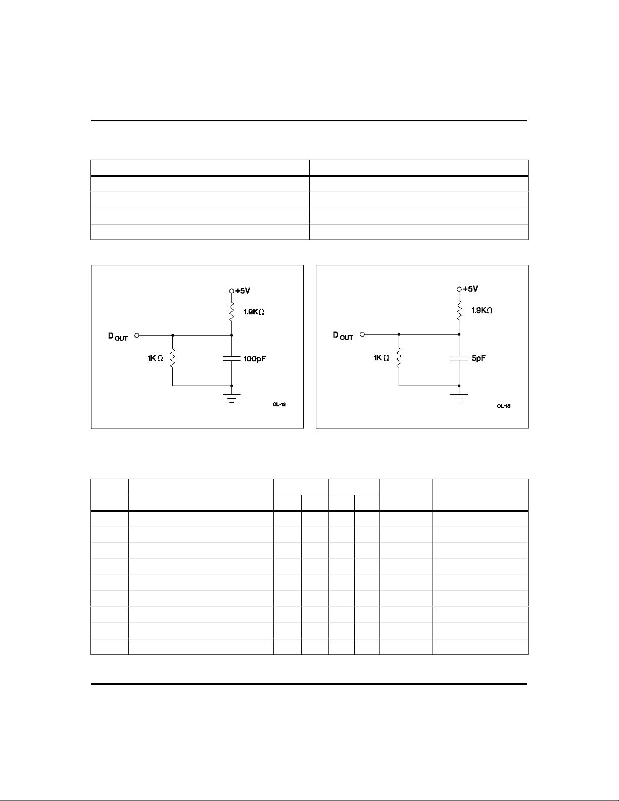
AC Test Conditions
Parameter Test Conditions
Input pulse levels 0V to 3.0V
Input rise and fall ti mes 5 ns
Input and output timing reference levels 1.5 V (unless otherwise specified)
Output load (including scope and jig) See Figures 1 and 2
Read Cycle (T
= 0 to 70°C, V
A
Symbol Parameter
t
t
t
t
t
t
t
t
t
RC
AA
ACE
OE
CLZ
OLZ
CHZ
OHZ
OH
Read cycle time 85 - 120 - ns
Address access time - 85 - 120 ns Output load A
Chip enable access t ime - 85 - 120 ns Out put load A
Output enable to output valid - 45 - 60 ns Output load A
Chip enable to output in low Z 5 - 5 - ns Output load B
Output enable to output in low Z 0 - 0 - ns Output load B
Chip disable to output in high Z 0 35 0 45 ns Output load B
Output disable to output in high Z 0 25 0 35 ns Output load B
Output hold from address change 10 - 10 - ns Output load A
CCmin
≤ VCC ≤ V
CCmax
-85
4
)
-120
Min. Max.
Figure 2. Output Load BFigure 1. Output Load A
Unit ConditionsMin. Max.
Sept. 1992
Page 5

bq4014/bq4014Y
Read Cycle No. 1 (Address Access)
Read Cycle No. 2 (CE Access)
Read Cycle No. 3 (OE Access)
1,3,4
1,5
1,2
Notes: 1. WE is held high for a read cycle.
2. Device is continuously selected:
3. Address is valid prior to or coincident with
4.
OE = VIL.
5. Device is continuously selected:
Sept. 1992
CE = OE = VIL.
CE transition low.
CE = VIL.
5
Page 6

bq4014/bq4014Y
Write Cycle (T
= 0 to 70°C, V
A
Symbol Parameter
t
WC
t
CW
t
AW
t
AS
t
WP
t
WR1
t
WR2
t
DW
t
DH1
t
DH2
t
WZ
t
OW
Write cycle time 85 - 120 - ns
Chip enable to end of write 75 - 100 - ns (1)
Address valid to end of write 75 - 100 - ns (1)
Address setup time 0 - 0 - ns
Write p ulse width 65 - 85 - ns
Write recove ry t ime
(write cycle 1)
Write recove ry t ime
(write cycle 2)
Data valid to end of write 35 - 45 - ns
Data hold time
(write cycle 1)
Data hold time
(write cycle 2)
Write enabled to output in
high Z
Output active from end of
write
CCmin
≤ VCC ≤ V
-85
Min. Max.
)
CCmax
-120
Min. Max.
Units Conditions/Notes
Measured from address valid to
beginning of write. (2)
Measured from beginning of write to
end of write. (1)
5-5-ns
15 - 15 - ns
Measured from
of write cycle. (3)
Measured from CE going high to end
of write cycle. (3)
Measured to first low-to-high
transition of e ither
0-0-ns
10 - 10 - ns
Measured from
of write cycle. (4)
Measured from CE going high to end
of write cycle. (4)
0 30 0 40 ns I/O pins are in output state. (5)
0 - 0 - ns I/O pins are in output state. (5)
WE going high to end
CE or WE.
WE going high to end
Notes: 1. A write ends at the earlier transition of
2. A wr ite occurs during the overlap of a low
of
CE going low and WE going lo w.
3. Either t
4. Either t
5. If
CE goes low simultaneou sl y with WE going low or after WE going low, the outputs remain in
WR1
DH1
or t
or t
DH2
must be met.
WR2
must be met.
high-impedance state.
CE going high and WE going high.
CE and a low WE. A write begins at the later transiti on
Sept. 1992
6
Page 7

bq4014/bq4014Y
Write Cycle No. 1 (WE-Controlled)
Write Cycle No. 2 (CE-Controlled)
1,2,3
1,2,3,4,5
Notes: 1. CE or WE must be high during address transition.
Sept. 1992
2. Because I/O may be active (
outputs must not be applied.
OE is high, the I/O pins remain in a state of high impedance.
3. If
4. Either t
5. Either t
WR1
DH1
or t
or t
DH2
must be met.
WR2
must be met.
OE low) during this period, data input signals of opposite polarity to the
7
Page 8

bq4014/bq40 14Y
Power-Down/Power-Up Cycle (T
= 0 to 70°C)
A
Symbol Parameter Minimum Typical Maximum Unit Conditions
t
PF
t
FS
t
PU
VCC slew, 4.75 to 4.25 V 300 - VCC slew, 4.25 to V
VCC slew, VSO to V
SO
(max.) 0 - -
PFD
10 - -
µs
µs
µs
Time during which
t
CER
Chip enable recovery time 40 80 120 ms
SRAM is write-protec ted
after V
passes V
CC
PFD
power-up.
t
t
DR
WPT
Data-retention time in
absence of V
CC
10 - - years TA = 25°C. (2)
Write-protect time 40 100 150
µs
Delay after V
down past V
CC
PFD
slews
before
SRAM is write-protec ted.
Notes: 1. Typi ca l va lu es in di c at e ope ra t io n a t T
2. Batteries are disconnected from circuit until after V
= 25°C, VCC = 5V.
A
CC
is applied for the first time. tDR is the
accumulated time in absence of power beginning when power is first applied to the device.
Caution: Negative undershoots below the absolute maximum rating of -0.3V in battery-backup mode
may affect data integrity.
Power-Down/Power-Up Timing
on
Sept. 1992
8
Page 9

bq4014/bq4014Y
Data Sheet Revision History (Sept. 1992 Changes From Sept. 1990)
Clarification of ICC test conditions, page 3.
MB: 32-Pin B-Type Module
32-Pin MB (B-Type Module
Dimension Minimum M ax im um
A 0.365 0.375
A1 0.015 -
B 0.017 0.023
C 0.008 0.013
D 2.070 2.100
E 0.710 0.740
e 0.590 0.630
G 0.090 0.110
L 0.120 0.150
S 0.275 0.310
All dimensions are in inches.
)
Sept. 1992
9
Page 10

bq4014/bq4014Y
Ordering Information
bq4014 MB -
Temperature:
blank = Commercial (0 to +70°C)
Speed Options:
85 = 85 ns
120 = 120 ns
Package Option:
MB = B-type module
Supply Tolerance:
no mark = 5% negative supply tolerance
Y = 10% negative su p p ly tolerance
Device:
bq4014 256K x 8 NVSRAM
10
Sept. 1992
Page 11

IMPORTANT NOTICE
T exas Instruments and its subsidiaries (TI) reserve the right to make changes to their products or to discontinue
any product or service without notice, and advise customers to obtain the latest version of relevant information
to verify, before placing orders, that information being relied on is current and complete. All products are sold
subject to the terms and conditions of sale supplied at the time of order acknowledgement, including those
pertaining to warranty, patent infringement, and limitation of liability.
TI warrants performance of its semiconductor products to the specifications applicable at the time of sale in
accordance with TI’s standard warranty. Testing and other quality control techniques are utilized to the extent
TI deems necessary to support this warranty . Specific testing of all parameters of each device is not necessarily
performed, except those mandated by government requirements.
CERTAIN APPLICATIONS USING SEMICONDUCTOR PRODUCTS MAY INVOLVE POTENTIAL RISKS OF
DEATH, PERSONAL INJURY, OR SEVERE PROPERTY OR ENVIRONMENTAL DAMAGE (“CRITICAL
APPLICATIONS”). TI SEMICONDUCTOR PRODUCTS ARE NOT DESIGNED, AUTHORIZED, OR
WARRANTED TO BE SUITABLE FOR USE IN LIFE-SUPPORT DEVICES OR SYSTEMS OR OTHER
CRITICAL APPLICA TIONS. INCLUSION OF TI PRODUCTS IN SUCH APPLICATIONS IS UNDERST OOD TO
BE FULLY AT THE CUSTOMER’S RISK.
In order to minimize risks associated with the customer’s applications, adequate design and operating
safeguards must be provided by the customer to minimize inherent or procedural hazards.
TI assumes no liability for applications assistance or customer product design. TI does not warrant or represent
that any license, either express or implied, is granted under any patent right, copyright, mask work right, or other
intellectual property right of TI covering or relating to any combination, machine, or process in which such
semiconductor products or services might be or are used. TI’s publication of information regarding any third
party’s products or services does not constitute TI’s approval, warranty or endorsement thereof.
Copyright 1999, Texas Instruments Incorporated
 Loading...