

Page 1
BQ21061
VINLS
PMID
LS/LDO
VDD
BAT
TS
+
±
NTC
GND
IN
VIO
Host
USB
I2C Bus
<150mA
Load
System
MR
PG
INT
LP
CE
C
4
C
5
C
3
C
2
C
1
Product
Folder
Order
Now
Technical
Documents
Tools &
Software
Support &
Community
BQ21061
SLUSDU0 –SEPTEMBER 2019
BQ21061 I2C Controlled 1-Cell 500-mA Linear Battery Charger With 10-nA Ship Mode,
Power Path With Regulated System (PMID) Voltage, And LDO
1 Features
1
• Linear battery charger with 1.25-mA to 500-mA
fast charge current range
– 0.5% Accurate I2C programmable battery
regulation voltage ranging from 3.6 V to 4.6 V
in 10-mV steps
– Configurable termination current supporting
down to 0.5 mA
– 20-V Tolerant input with typical 3.4-V to 5.5-V
input voltage operating range
– Programmable thermal charging profile, fully
configurable hot, warm, cool and cold
thresholds
• Power Path management for powering system
and charging battery
– I2C Programmable regulated system voltage
(PMID) ranging from 4.4V to 4.9V in addition to
battery voltage tracking and Input pass-though
options
– Dynamic power path management optimizes
charging from weak adapters
– Advanced I2C control allows host to disconnect
the battery or adapter as needed
• I2C Configurable load switch or up to 150-mA
LDO output
– Programmable range from 0.6 V to 3.7 V in
100-mV steps
• Ultra low Iddq for extended battery life
– 10-nA Ship mode battery Iq
– 400-nA Iq While powering the system (PMID
and VDD on)
• One push-button wake-up and reset input with
adjustable timers
– Supports system power cycle and HW reset
• 20-Pin 2-mm x 1.6-mm CSP package
• 11-mm2Total solution size
1
2 Applications
• Headsets, earbuds and hearing aids
• Smart watches and smart trackers
• Wearable fitness and activity monitors
• Blood glucose monitors
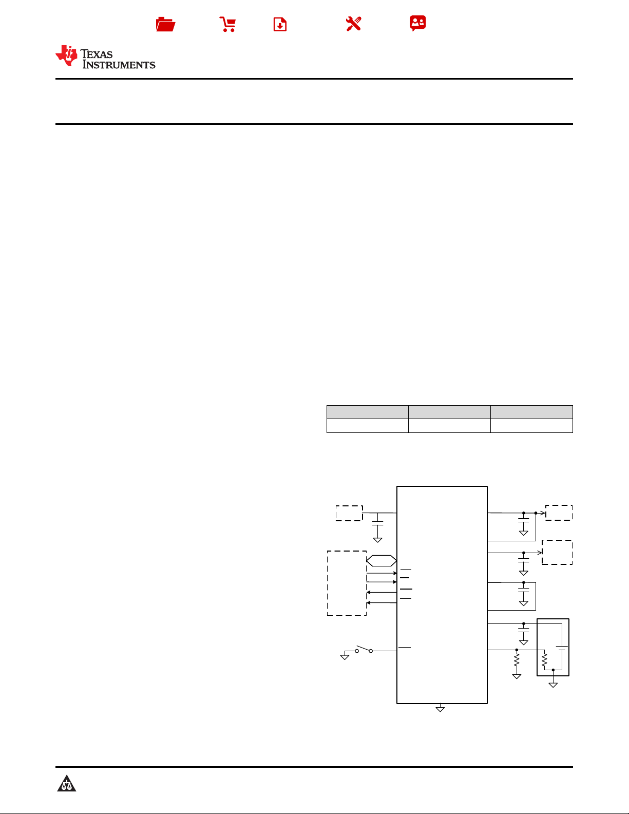
3 Description
The BQ21061 is a highly integrated battery charge
management IC that integrates the most common
functions for wearable, portable and small medical
devices, namely a charger, a regulated output voltage
rail for system power, a LDO, and push-button
controller.
The BQ21061 IC integrates a linear charger with
PowerPath that enables quick and accurate charging
for small batteries while providing a regulated voltage
to the system. The regulated system voltage (PMID)
output may be configured through I2C based on the
recommended operating condition of downstream
IC's and system loads for optimal system operation.
Device Information
PART NUMBER PACKAGE BODY SIZE (NOM)
BQ21061 DSBGA (20) 2.00 mm x 1.60 mm
(1) For all available packages, see the orderable addendum at
the end of the data sheet.
Simplified Schematic
(1)
An IMPORTANT NOTICE at the end of this data sheet addresses availability, warranty, changes, use in safety-critical applications,
intellectual property matters and other important disclaimers. PRODUCTION DATA.
Page 2

BQ21061
SLUSDU0 –SEPTEMBER 2019
www.ti.com
Table of Contents
1 Features.................................................................. 1
2 Applications ........................................................... 1
3 Description ............................................................. 1
4 Revision History..................................................... 2
5 Pin Configuration and Functions......................... 3
6 Specifications......................................................... 4
6.1 Absolute Maximum Ratings...................................... 4
6.2 ESD Ratings.............................................................. 4
6.3 Recommended Operating Conditions....................... 4
6.4 Thermal Information.................................................. 5
6.5 Electrical Characteristics........................................... 5
6.6 Timing Requirements................................................ 7
6.7 Typical Characteristics.............................................. 9
7 Detailed Description............................................ 12
7.1 Overview................................................................. 12
7.2 Functional Block Diagram....................................... 12
7.3 Feature Description................................................. 13
7.4 Device Functional Modes........................................ 26
4 Revision History
DATE REVISION NOTES
September 2019 * Initial release
7.5 Register Map .......................................................... 29
8 Application and Implementation ........................ 48
8.1 Application Information............................................ 48
8.2 Typical Application ................................................. 48
9 Power Supply Recommendations...................... 53
10 Layout................................................................... 53
10.1 Layout Guidelines ................................................. 53
10.2 Layout Example .................................................... 53
11 Device and Documentation Support................. 54
11.1 Device Support...................................................... 54
11.2 Documentation Support ....................................... 54
11.3 Receiving Notification of Documentation Updates 54
11.4 Support Resources ............................................... 54
11.5 Trademarks........................................................... 54
11.6 Electrostatic Discharge Caution............................ 54
11.7 Glossary................................................................ 54
12 Mechanical, Packaging, and Orderable
Information........................................................... 54
2
Submit Documentation Feedback Copyright © 2019, Texas Instruments Incorporated
Product Folder Links: BQ21061
Page 3
IN PMID BAT GND
/PG PMID BAT TS
/MR /CE NC1 NC2
VDD /INT /LP LSLDO
VIO SDA SCL VINLS
A
B
C
D
E
1 2 3 4
www.ti.com
5 Pin Configuration and Functions
BQ21061
SLUSDU0 –SEPTEMBER 2019
YFP Package
20-Pin DSBGA
Top View
Pin Functions
PIN
NAME NO.
IN A1 I
PMID A2, B2 I/O
GND A4 PWR Ground connection. Connect to the ground plane of the circuit.
VDD D1 O Digital supply LDO. Connect a 2.2-µF from this pin to ground.
CE C2 I
SCL E3 I/O I2C Interface Clock. Connect SCL to the logic rail through a 10-kΩ resistor.
SDA E2 I I2C Interface Data. Connect SDA to the logic rail through a 10-kΩ resistor.
LP D3 I
INT D2 O
MR C1 I
LS/LDO D4 O
VINLS E4 I
BAT A3, B3 I/O
I/O DESCRIPTION
DC Input Power Supply. IN is connected to the external DC supply. Bypass IN to GND with
at least 1-µF of capacitance using a ceramic capacitor.
Regulated System Output. Connect 22-µF capacitor from PMID to GND as close to the PMID
and GND pins as possible. If operating in VIN Pass-Through Mode (PMID_REG = 111) a
lower capacitor value may be used (at least 3-µF of ceramic capacitance with DC bias derating).
Charge Enable. Drive CE low or leave disconnected to enable charging when VIN is valid.
CE is pulled low internally with 900-kΩ resistor.
Low Power Mode Enable. Drive this pin low to enable the device in low power mode when
powered by the battery. LP is pulled low internally with 900-kΩ resistor.
INT is an open-drain output that signals fault interrupts. When a fault occurs, a 128-µs pulse
is sent out as an interrupt for the host.
Manual Reset Input. MR is a general purpose input used to reset the device or to wake it up
from Ship Mode. MR has in internal 125-kΩ pull-up resistor to BAT.
Load Switch or LDO output. Connect 2.2 µF of ceramic capacitance to this pin to assure
stability. Be sure to account for capacitance bias voltage derating when selecting the
capacitor.
Input to the Load Switch / LDO output. Connect at least 1 µF of ceramic capacitance from
this pin to ground.
Battery Connection. Connect to the positive terminal of the battery. Bypass BAT to GND with
at least 1 µF of ceramic capacitance.
Submit Documentation FeedbackCopyright © 2019, Texas Instruments Incorporated
Product Folder Links: BQ21061
3
Page 4
BQ21061
SLUSDU0 –SEPTEMBER 2019
www.ti.com
Pin Functions (continued)
PIN
NAME NO.
TS B4 I
PG B1 O
VIO E1 I
NC1 C3 I
NC2 C4 I
I/O DESCRIPTION
Battery Pack NTC Monitor. Connect TS to a 10-kΩ NTC thermistor in parallel to a 10-kΩ
resistor. If TS function is not to be used connect a 5-kΩ resistor from TS to ground.
Open-drain Power Good status indication output. The PG pin can also be configured as a
general purpose open drain output or level shifter version of MR.
System IO supply. Connect to system IO supply to allow level shifting of input signals (SDA,
SCL, LP and CE) to the device internal digital domain. Connect to VDD when external IO
supply is not available.
No Connect. Connect to ground if possible for better thermal dissipation or leave floating. Do
not connect to a any voltage source or signal to avoid higher quiescent current.
No Connect. Connect to ground if possible for better thermal dissipation. May be shorted to
/LP for easier routing as long as Absolute Maximum Rating requirements are met..
6 Specifications
6.1 Absolute Maximum Ratings
over operating free-air temperature range (unless otherwise noted)
IN –0.3 20 V
Voltage
Current
Junction temperature, T
Storage temperature, T
(1) Stresses beyond those listed under Absolute Maximum Rating may cause permanent damage to the device. These are stress ratings
only, which do not imply functional operation of the device at these or any other conditions beyond those indicated under Recommended
Operating Condition. Exposure to absolute-maximum-rated conditions for extended periods may affect device reliability.
TS,VDD, NC –0.3 1.95 V
All other pins –0.3 5.5 V
IN 0 800 mA
BAT, PMID –0.5 1.5 A
INT, PG 0 10 mA
J
stg
(1)
MIN MAX UNIT
–40 125 °C
–55 150 °C
6.2 ESD Ratings
Human body model (HBM), per
V
(ESD)
Electrostatic discharge
ANSI/ESDA/JEDEC JS-001, all pins
Charged device model (CDM), per JEDEC
specification JESD22-C101, all pins
(1) JEDEC document JEP155 states that 500-V HBM allows safe manufacturing with a standard ESD control process.
(2) JEDEC document JEP157 states that 250-V CDM allows safe manufacturing with a standard ESD control process.
(1)
(2)
6.3 Recommended Operating Conditions
over operating free-air temperature range (unless otherwise noted)
MIN NOM MAX UNIT
V
BAT
V
IN
V
INLS
V
IO
I
LDO
I
PMID
T
A
(1) Based on minimum V
4
Battery voltage range 2.4 4.6 V
Input voltage range 3.15 5.25
LDO input voltage range 2.2 5.25
IO supply voltage range 1.2 3.6 V
LDO output current 0 100 mA
PMID output current 0 500 mA
Operating free-air temperature range –40 85 °C
value. 5.5V under typical conditions
OVP
Submit Documentation Feedback Copyright © 2019, Texas Instruments Incorporated
Product Folder Links: BQ21061
VALUE UNIT
±2000
V
±500
(1)
(1)
V
V
Page 5
BQ21061
www.ti.com
SLUSDU0 –SEPTEMBER 2019
6.4 Thermal Information
BQ21061
THERMAL METRIC
(1)
UNITYFP (DSBGA)
20-PIN
R
θJA
R
θJA
R
θJC(top)
R
θJB
Ψ
JT
Ψ
JB
R
θJC(bot)
Junction-to-ambient thermal resistance
Junction-to-ambient thermal resistance 74.4 °C/W
Junction-to-case (top) thermal resistance 0.5 °C/W
Junction-to-board thermal resistance 17.6 °C/W
Junction-to-top characterization parameter 0.3 °C/W
Junction-to-board characterization parameter 17.7 °C/W
Junction-to-case (bottom) thermal resistance N/A °C/W
(2)
36.1 °C/W
(1) For more information about traditional and new thermal metrics, see the Semiconductor and IC Package Thermal Metrics application
report.
(2) Measured in BQ21061EVM board.
6.5 Electrical Characteristics
VIN= 5V, V
INPUT CURRENTS
I
IN
I
BAT_SHIP
I
BAT_LP
I
BAT_ACTI
VE
POWER PATH MANAGEMENT AND INPUT CURRENT LIMIT
V
PMID_RE
G
V
PMID_RE
G_ACC
R
ON(IN-
PMID)
V
BSUP1
V
BSUP2
I
ILIM
V
IN_DPM
BATTERY CHARGER
V
DPPM
= 3.6V. TJ= 25°C unless otherwise noted.
BAT
PARAMETER TEST CONDITIONS MIN TYP MAX UNIT
PMID_MODE = 01, VIN= 5V, V
Input supply current
3.6V
VIN= 5V, V
Battery Discharge Current in Ship Mode VIN= 0V , V
Battery Quiescent Current in Low-power
Mode
Battery Quiescent Current in Active
Mode
VIN= 0V , V
VIN= 0V , V
VIN= 0V , V
VIN= 0V , V
Default System (PMID) Regulation
Voltage
VIN= 5V, V
System Regulation Voltage Accuracy
100mA, TJ= 25°C
VIN= 5V, V
500mA
I
= 500mA (ILIM = 110), VIN= 5V, I
Input FET ON resistance
Enter supplements mode threshold
Exit supplements mode threshold
ILIM
= 150mA
V
> V
BAT
BAT
> V
BATUVLO
BATUVLO
Charge disabled
V
Charge disabled
= 3.6V Charge Disabled 1.6 mA
BAT
= 3.6V 10 nA
BAT
= 3.6V, LDO Disabled 0.46 0.9 µA
BAT
= 3.6V, LDO Enabled 1.7 1.9 µA
BAT
= 3.6V, LDO Disabled 18 23 µA
BAT
= 3.6V, LDO Enabled 21 25 µA
BAT
PMID_REG
PMID_REG
= 4.5V. I
= 4.5V. I
, DPPM enabled or
, DPPM enabled or
PMID
PMID
BAT
=
=
= 0-
500 µA
4.5 V
-1 1 %
–3 3 %
IN
280 520 mΩ
V
<
PMID
V
–
BAT
40mV
V
<
PMID
V
–
BAT
20mV
mV
mV
Programmable Range 50 600 mA
I
= 50mA 45 50 mA
ILIM
Input Current Limit
Input DPM voltage threshold where
current in reduced
I
= 100mA 90 100 mA
ILIM
I
= 150mA 135 150 mA
ILIM
I
= 500mA 450 500 mA
ILIM
Programmable Range 4.2 4.9 V
Accuracy –3 3 %
PMID voltage threshold when charge
current is reduced
V
PMID
- V
BAT
200 mV
Product Folder Links: BQ21061
Submit Documentation FeedbackCopyright © 2019, Texas Instruments Incorporated
5
Page 6
BQ21061
SLUSDU0 –SEPTEMBER 2019
Electrical Characteristics (continued)
www.ti.com
VIN= 5V, V
= 3.6V. TJ= 25°C unless otherwise noted.
BAT
PARAMETER TEST CONDITIONS MIN TYP MAX UNIT
R
ON(BAT-
PMID)
V
BATREG
Battery Discharge FET On Resistance V
Charge Voltage Programmable charge voltage range 3.6 4.6 V
Voltage Regulation Accuracy 0.5 0.5 %
Fast Charge Programmable Current
I
CHARGE
Range
Fast Charge Current Accuracy I
I
PRECHAR
GE
I
TERM
Precharge current Precharge current programmable range 1.25 77.5 mA
Precharge Current Accuracy -40°C < TJ< 85°C –10 10 %
Termination Charge Current
Accuracy I
V
LOWV
V
SHORT
I
SHORT
V
RCH
R
PMID_PD
Programmable voltage threshold for precharge to fast charge transitions
Battery voltage threshold for short
detection
Charge Current in Battery Short
Condition
Recharge Threshold voltage
PMID pull-down resistance V
VDD
V
DD
VDD LDO output voltage 1.8 V
LS/LDO
Input voltage range for Load switch
Mode
V
INLS
Input voltage range for LDO Mode
LDO programmable output voltage range 0.6 3.7 V
V
LDO
ΔV
OUT
ΔV
V
IN
R
DOSN_L
DO
R
DSCH_LS
LDO
I
OCL_LDO
LDO output accuracy
/ΔI
OUT
DC Load Regulation
/Δ
OUT
DC Line Regulation
Switch On resistance V
Discharge FET On-resistance for LS V
Output Current Limit V
LDO VINLS quiescent current in LDO
I
IN_LDO
mode
OFF State Supply Current V
BATTERY PACK NTC MONITOR
V
HOT
V
WARM
V
COOL
High temperature threshold VTSfalling, -10°C < TJ< 85°C 0.182
Warm temperature threshold VTSfalling, -10°C < TJ< 85°C 0.262
Cool temperature threshold VTSrising, -10°C < TJ< 85°C 0.510
= 4.35V, I
BAT
V
< V
LOWV
CHARGE
BAT
> 5mA –5 5 %
Termination Current Programmable
Range
= 10% I
TERM
= 100mA 100 175 mΩ
BAT
< V
BATREG
1.25 500 mA
1 31 %
CHARGE
, I
CHARGE
= 100mA –5
(1)
(1)
5
VBAT rising. Programmable Range 2.8 3 V
VBAT falling, VIN = 5V 2.41 2.54 2.67 V
I
V
< V
BAT
SHORT
V
falling, V
BAT
140mV setting
V
falling, V
BAT
200mV setting
= 3.6V 25 Ω
PMID
BATREG
BATREG
= 4.2V, V
= 4.2V, V
RCH
RCH
=
=
PRECHAR
GE
140 mV
200 mV
mA
0.8 5.5 V
2.2 or
V
LDO
500mV
+
5.5 V
TJ= 25°C –2 2 %
V
= 1.8V, V
LDO
0°C < TJ< 85°C, 1 mA < I
V
= 1.8V
LDO
0°C < TJ< 85°C, Over V
= 100mA, V
= 3.6V 250 450 mΩ
INLS
= 3.6V 40 Ω
INLS
= 0V 200 300 mA
LS/LDO
V
= V
BAT
INLS
= V
BAT
INLS
LDO
INLS
= 1.8V
=3.6V. I
= 1mA –3 3 %
LOAD
< 150mA,
INLS
OUT
range, I
OUT
1.2 %
0.5 %
=3.6V 0.9 µA
=3.6V 0.25 µA
(1)
(1)
(1)
0.185 0.189
0.265 0.268
0.514 0.518
(1)
(1)
(1)
%
V
V
V
(1) Based on Characterization Data
6
Submit Documentation Feedback Copyright © 2019, Texas Instruments Incorporated
Product Folder Links: BQ21061
Page 7
www.ti.com
Electrical Characteristics (continued)
BQ21061
SLUSDU0 –SEPTEMBER 2019
VIN= 5V, V
= 3.6V. TJ= 25°C unless otherwise noted.
BAT
PARAMETER TEST CONDITIONS MIN TYP MAX UNIT
V
COLD
V
OPEN
V
HYS
I
TS_BIAS
Cold temperature threshold VTSrising, -10°C < TJ< 85°C 0.581
TS Open threshold VTSrising, -10°C < TJ< 85°C 0.9 V
Threshold hysteresis 4.7 mV
TS bias current -10°C < TJ< 85°C 78.4 80 81.6 µA
PROTECTION
V
UVLO
IN active threshold voltage
Battery undervoltage Lockout Threshold
Voltage
V
BATUVLO
Accuracy –3 3 %
Battery undervoltage Lockout Threshold
Voltage at Power Up
V
SLP_ENT
RY
V
SLP_EXIT
V
OVP
Sleep Entry Threshold (VIN- V
Sleep Exit Threshold (VIN- V
Input Supply Over Voltage Threshold
Battery Over Current Threshold
I
BAT_OCP
Programmable range
Current Limit Accuracy –30 30 %
T
SHUTDO
WN
T
HYS
Thermal shutdown trip point 125 °C
Thermal shutdown trip point hysteresis 15 °C
I2C INTERFACE (SCL and SDA)
I2C Frequency 100 400 kHz
V
V
V
I
IL
IH
OL
LKG
Input Low threshold level V
Input High Threshold level V
Output Low threshold level V
High-level leakage Current V
/MR INPUT
R
PU
V
IL
Internal pull up resistance 90 125 170 kΩ
/MR Input Low threshold level V
/INT, /PG OUTPUTS
V
I
OL
LKG
Output Low threshold level V
/INT Hi level leakage Current High Impedance, V
/CE, /LP INPUTS
R
PDOWN
V
IL
V
IH
/CE pull down resistance 900 kΩ
Input Low threshold level VIO= 1.8V 0.45 V
/CE Input High Threshold level VIO= 1.8V 1.35 V
) 2.0V < V
BAT
) 2.0V < V
BAT
(1)
0.585 0.589
(1)
VINrising 3.4 V
VINfalling 3.25 V
Programmable range, 150 mV
Hysteresis
V
rising, VIN= 0V, TJ= 25°C 3.15 V
BAT
BAT
BAT
< V
< V
, VINfalling 80 mV
BATREG
BATREG
2.4 3 V
130 mV
VINrising 5.35 5.5 5.8 V
VINfalling (125mV hysteresis) 5.4 V
I
BAT_OCP
increasing 1200 1600 mA
= VIO= 1.8V
PULLUP
= VIO= 1.8V
PULLUP
= VIO= 1.8V, I
PULLUP
= VIO= 1.8V 1 µA
PULLUP
> V
BAT
BUVLO
= VIO= 1.8V, I
PULLUP
PULLUP
= 5mA
LOAD
= 5mA
LOAD
= VIO= 1.8V 1 µA
0.75 *
V
IO
0.25 *
V
IO
0.25 *
V
IO
0.3 V
0.25 *
V
IO
V
V
V
V
V
6.6 Timing Requirements
PARAMETER TEST CONDITIONS MIN TYP MAX UNIT
BATTERY CHARGE TIMERS
t
MAXCHG
t
PRECHG
Charge safety timer Programmable range 180 720 min
Precharge safety timer 0.25 * t
Product Folder Links: BQ21061
MAXCHG
Submit Documentation FeedbackCopyright © 2019, Texas Instruments Incorporated
7
Page 8
BQ21061
SLUSDU0 –SEPTEMBER 2019
Timing Requirements (continued)
PARAMETER TEST CONDITIONS MIN TYP MAX UNIT
WATCHDOG TIMERS
t
WATCHDO
G_SW
t
HW_RESE
T_WD
LDO
t
ON_LDO
t
OFF_LDO
t
PMID_LDO
_DELAY
PUSHBUTTON TIMERS (/MR)
t
WAKE1
t
WAKE2
t
RESET_W
ARN
t
HW_RESE
T
t
RESTART(
AUTOWAK
E)
PROTECTION
t
DGL_SLP
t
DGL_OVP
t
DGL_OCP
t
REC_SC
t
RETRY_S
C
t
DGL_SHT
DWN
I2C INTERFACE
t
WATCHDO
G
t
I2CRESET
INPUT PINS (/CE and /LP)
t
LP_EXIT_I
2C
SW Watchdog timer 25 50 s
HW reset watchdog timer WATCHDOG_15S_ENABLE = 1 15 s
Turn ON time 100mA load, to 90% V
Turn OFF time 100mA load, to 10% V
Delay between PMID and LDO enable
during power up
WAKE1 Timer. Timer for Ship Mode
wake.
WAKE2 Timer. Time from /MR falling
edge to INT being asserted.
RESET_WARN Timer. Time prior to HW
RESET
HW RESET Timer. Time from /MR falling
edge to HW Reset
RESTART Timer. Time from /MR HW
Reset to PMID power up
Deglitch time for supply rising above
V
+ V
SLP
SLP_HYS
Deglitch time for V
Threshold VIN falling below V
OVP
Battery OCP deglitch time 30 µs
Recovery time, BAT Short Circuit during
Discharge Mode
Retry window for PMID or BAT short
circuit recovery
Deglitch time, Thermal shutdown TJrising above T
I2C interface reset timer for host When enabled 50 s
I2C interface inactive reset timer 500 ms
Time for device to exit Low-power mode
and allow I2C communication
www.ti.com
LDO
LDO
500 µs
30 µs
Startup 20 ms
MR_WAKE1_TIMER = 0 106 125 144 ms
MR_WAKE2_TIMER = 1 1.7 2 2.3 s
MR_RESET_WARN = 01 0.85 1 1.15 s
MR_HW_RESET = 01 6.8 8 9.2 s
AUTOWAKE = 01 1.05 1.2 1.35 s
120 µs
OVP
32 ms
250 ms
2 s
SHUTDOWN
10 µs
VIN= 0V. 1 ms
8
Submit Documentation Feedback Copyright © 2019, Texas Instruments Incorporated
Product Folder Links: BQ21061
Page 9
V
INLS
(V)
R
DSON
(:)
1 1.5 2 2.5 3 3.5 4 4.5 5
0
0.2
0.4
0.6
0.8
1
1.2
D015
TJ = -40C
TJ = 25C
TJ = 85C
I
LOAD
(A)
V
LDO
(V)
0.1 0.11 0.12 0.13 0.14 0.15 0.16 0.17 0.18 0.19 0.2
0.7984
0.7992
0.8
0.8008
0.8016
0.8024
0.8032
0.804
0.8048
0.8056
0.8064
D009
TJ = -40C
TJ = 25C
TJ = 85C
I
PRECHARGE
(A)
Error (%)
0 5 10 15 20 25 30 35 40 45 50 55 60 65 70 75 80
-1.2
-1
-0.8
-0.6
-0.4
-0.2
0
0.2
0.4
0.6
0.8
1
1.2
D013
TJ = 25C
TJ = 0C
TJ = -40C
TJ = 60C
TJ = 125C
I
PRECHARGE
(mA)
Error (%)
0 5 10 15 20 25 30 35 40
-1.5
-1
-0.5
0
0.5
1
1.5
D012
TJ = 25C
TJ = 0C
TJ = -40C
TJ = 60C
TJ = 125C
V
BATREG
(V)
Error (%)
3.6 3.7 3.8 3.9 4 4.1 4.2 4.3 4.4 4.5 4.6
-0.5
-0.45
-0.4
-0.35
-0.3
-0.25
-0.2
-0.15
-0.1
-0.05
0
D011
TJ = 25C
TJ = 0C
TJ = -40C
TJ = 60C
TJ = 125C
I
CHARGE
(A)
Error (%)
0 0.05 0.1 0.15 0.2 0.25 0.3 0.35 0.4 0.45 0.5
-1.75
-1.5
-1.25
-1
-0.75
-0.5
-0.25
0
0.25
0.5
0.75
1
1.25
D014
TJ = -40C
TJ = 0C
TJ = 25C
TJ = 60C
TJ = 125C
www.ti.com
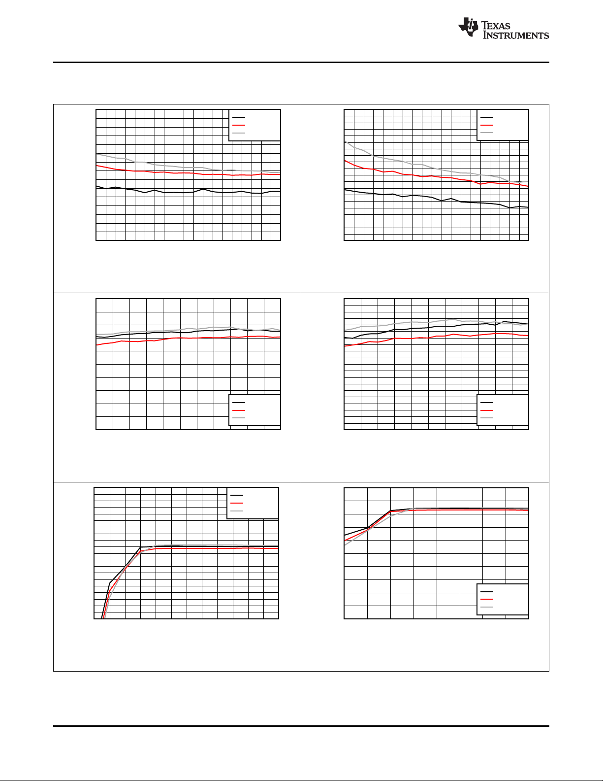
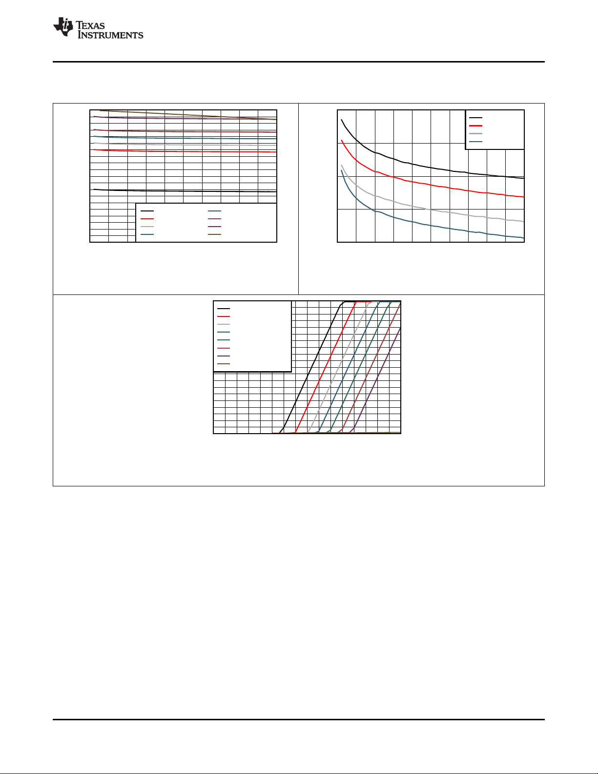
6.7 Typical Characteristics
CIN= 1 µF, C
= 10 µF, C
PMID
LSLDO
= 2.2 µF, C
= 1 µF (unless otherwise specified)
BAT
BQ21061
SLUSDU0 –SEPTEMBER 2019
VIN = 5 V PMID_REG_CTRL = 111 (Pass-Through)
Figure 1. Battery Regulation Voltage Accuracy vs.
VBATREG Setting
VIN = 5 V VBAT = 2.7 V ICHARGE_RANGE = 0
Figure 3. Pre-Charge Current Accuracy vs. IPRECHARGE
setting (ICHARGE_RANGE = 0)
VIN = 5 V VBAT = 3.6 V ICHARGE_RANGE = 1
Figure 2. Charge Current Accuracy vs. ICHARGE Setting
VBUS = 5 V VBAT = 2.7 V ICHARGE_RANGE = 1
Figure 4. Pre-Charge Current Accuracy vs. IPRECHARGE
Setting (ICHARGE_RANGE = 1)
VBUS = 5 V
Figure 5. LS/LDO Switch On Resistance vs. VINLS
Product Folder Links: BQ21061
VIN = 0 V VBAT = 3.6 V VINLS = VPMID
Figure 6. LDO Load Regulation (VLDO = 0.8 V)
Submit Documentation FeedbackCopyright © 2019, Texas Instruments Incorporated
9
Page 10
V
INLS
(V)
VLDO (V)
3.2 3.3 3.4 3.5 3.6 3.7 3.8 3.9 4 4.1 4.2 4.3 4.4
3.2
3.22
3.24
3.26
3.28
3.3
3.32
3.34
3.36
3.38
3.4
D006
TJ = -40C
TJ = 25C
TJ = 85C
V
INLS
(V)
V
LDO
(V)
3.6 3.7 3.8 3.9 4 4.1 4.2 4.3 4.4
3.4
3.425
3.45
3.475
3.5
3.525
3.55
3.575
3.6
3.625
3.65
D007
TJ = -40C
TJ = 25C
TJ = 85C
V
INLS
(V)
V
LDO
(V)
2.2 2.4 2.6 2.8 3 3.2 3.4 3.6 3.8 4 4.2 4.4
1.19
1.192
1.194
1.196
1.198
1.2
1.202
1.204
1.206
1.208
1.21
D004
TJ = -40C
TJ = 25C
TJ = 85C
V
INLS
(V)
V
LDO
(V)
2.2 2.4 2.6 2.8 3 3.2 3.4 3.6 3.8 4 4.2 4.4
1.79
1.792
1.794
1.796
1.798
1.8
1.802
1.804
1.806
1.808
1.81
D005
TJ = -40C
TJ = 25C
TJ = 85C
I
LOAD
(A)
V
LDO
(V)
0.01 0.03 0.05 0.07 0.09 0.11 0.13 0.15 0.17 0.19
1.79
1.792
1.794
1.796
1.798
1.8
1.802
1.804
1.806
1.808
1.81
1.812
1.814
1.816
1.818
1.82
D008
TJ = -40C
TJ = 25C
TJ = 85C
I
LOAD
(A)
V
LDO
(V)
0.01 0.03 0.05 0.07 0.09 0.11 0.13 0.15 0.17 0.19
3.29
3.294
3.298
3.302
3.306
3.31
3.314
3.318
3.322
3.326
3.33
D010
TJ = -40C
TJ = 25C
TJ = 85C
BQ21061
SLUSDU0 –SEPTEMBER 2019
Typical Characteristics (continued)
www.ti.com
CIN= 1 µF, C
= 10 µF, C
PMID
LSLDO
= 2.2 µF, C
= 1 µF (unless otherwise specified)
BAT
VIN = 0 V VBAT = 3.6 V VINLS = VPMID
Figure 7. LDO Load Regulation (VLDO = 1.8 V)
VIN = 0 V VBAT = 3.6 V VINLS= VPMID
Figure 8. LDO Load Regulation (VLDO = 3.3 V)
VBAT = 4.4 V ILOAD = 150 mA
Figure 9. LDO Line Regulation (VLDO = 1.2 V)
10
VBAT = 4.4 V ILOAD = 150 mA
Figure 11. LDO Line Regulation (VLDO = 3.3 V)
Submit Documentation Feedback Copyright © 2019, Texas Instruments Incorporated
VBAT = 4.4 V ILOAD = 150 mA
Figure 10. LDO Line Regulation (VLDO = 1.8 V)
VBAT = 4.4 V ILOAD = 150 mA
Figure 12. LDO Line Regulation (VLDO = 3.6 V)
Product Folder Links: BQ21061
Page 11
Temperature(qC)
Charge Current Reduction (%)
50 60 70 80 90 100 110 120 130
0
10
20
30
40
50
60
70
80
90
100
D004
THERM_REG = 0
THERM_REG = 1
THERM_REG = 2
THERM_REG = 3
THERM_REG = 4
THERM_REG = 5
THERM_REG = 6
THERM_REG = 7
PMID Load Current (A)
V
PMID
(V)
0 0.05 0.1 0.15 0.2 0.25 0.3 0.35 0.4 0.45 0.5
3
3.2
3.4
3.6
3.8
4
4.2
4.4
4.6
4.8
5
D001
PMID_REG = 0
PMID_REG = 1
PMID_REG = 2
PMID_REG = 3
PMID_REG = 4
PMID_REG = 5
PMID_REG = 6
PMID_REG = 7
PMID Load (A)
V
PMID
(V)
0 0.05 0.1 0.15 0.2 0.25 0.3 0.35 0.4 0.45 0.5
4.44
4.46
4.48
4.5
4.52
D003
TJ = -40°C
TJ = 25°C
TJ = 85°C
TJ = 125°C
www.ti.com
Typical Characteristics (continued)
BQ21061
SLUSDU0 –SEPTEMBER 2019
CIN= 1 µF, C
= 10 µF, C
PMID
LSLDO
= 2.2 µF, C
VBAT = 0 V
Figure 13. PMID Load Regulation
= 1 µF (unless otherwise specified)
BAT
Figure 14. PMID Load Regulation vs. Temperature
VBAT = 3.6 V VIN = 5 V
VBAT = 3.6 V VIN = 5 V
Figure 15. Charge Current Thermal Regulation
Product Folder Links: BQ21061
Submit Documentation FeedbackCopyright © 2019, Texas Instruments Incorporated
11
Page 12
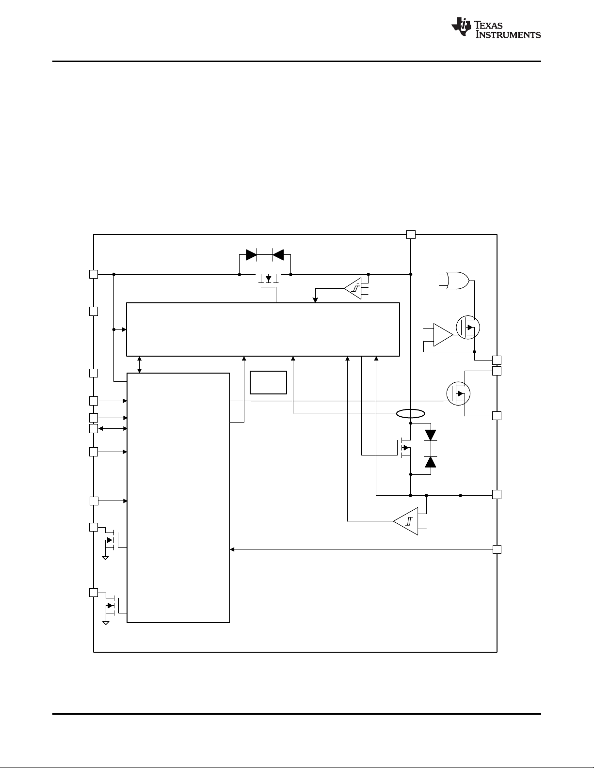
LDO, and BAT FET Control
Device Control
V
IN
Charge
Enable
I2C
Interface
Low Power Mode
Control
Charge Control
LDO / Load Switch
Control
Thermal
Shutdown
I
BATREG
LDO
Control
UVLO
V
BATREG
V
IN_DPM
BAT
VIN
+
±
/Power Good
GP Output
Interrupt
JEITA/Temp
Information
For Charge Control
S
G
D
S
G
D
Q7
Q8
IN
GND
VIO
/CE
SCL
SDA
/LP
/MR
/INT
/PG
PMID
VDD
VINLS
LDO
BAT
TS
V
BATUVLO
Q5/Q6
1.045 x V
BAT
PMID_REG
BQ21061
SLUSDU0 –SEPTEMBER 2019
www.ti.com
7 Detailed Description
7.1 Overview
The BQ21061 IC is a highly programmable battery management device that integrates a 500-mA linear charger
for single cell Li-Ion batteries, a general purpose LDO that may be configured as a load switch, and a pushbutton controller. Through it's I2C interface the host may change charging parameters such as battery regulation
voltage and charge current, and obtain detailed device status and fault information. The push-button controller
allows the user to reset the system without any intervention from the host and wake up the device from Ship
Mode.
7.2 Functional Block Diagram
12
Submit Documentation Feedback Copyright © 2019, Texas Instruments Incorporated
Product Folder Links: BQ21061
Page 13
V
BAT
< V
LOWV
Start Precharge
Icharge set by I2C
Connect VIN
Precharge safety
timer expired?
Stop Charging and set
Fault bits
/CE toggled or VIN and
removed and
reconnected?
V
BAT
> V
LOWV
Start FastCharge
Icharge set by I2C
I
BAT
< I
TERM
Fast Charge safety
timer expired?
Charge Done (Set bit
and interrupt and
disconnect BATFET)
V
BAT
< V
BAT
- V
RCH
Yes
No
Yes
No
Yes
No
Yes
No
Yes
No
Yes
No
Yes No
BQ21061
www.ti.com
SLUSDU0 –SEPTEMBER 2019
7.3 Feature Description
7.3.1 Linear Charger and Power Path
The BQ21061 IC integrates a linear charger that allows the battery to be charged with a programmable charge
current of up to 500 mA. In addition to the charge current, other charging parameters can be programmed
through I2C such as the battery regulation voltage, pre-charge current, termination current, and input current limit
current.
The power path allows the system to be powered from PMID, even when the battery is dead or charging, by
drawing power from IN pin. It also prioritizes the system load connected to PMID, reducing the charging current,
if necessary, in order support the load when input power is limited. If the input supply is removed and the battery
voltage level is above V
BATUVLO
A more detailed description of the charger functionality is presented in the following sections of this document.
7.3.1.1 Battery Charging Process
The following diagram summarizes the charging process of the BQ21061 charger.
, PMID will automatically and seamlessly switch to battery power.
Figure 16. BQ21061 Charger Flow Diagram
Submit Documentation FeedbackCopyright © 2019, Texas Instruments Incorporated
13
Product Folder Links: BQ21061
Page 14
BQ21061
SLUSDU0 –SEPTEMBER 2019
Feature Description (continued)
www.ti.com
When a valid input source is connected (VIN> V
UVLO
and V
BAT+VSLP
< VIN< V
), the state of the CE pin
OVP
determines whether a charge cycle is initiated. When the CE input is high and a valid input source is connected,
the battery charge FET is turned off, preventing any kind of charging of the battery. A charge cycle is initiated
when the CHARGE_DISABLE bit is written to 0 and CE pin in low. Table 1 shows the CE pin and bit priority to
enable/disable charging.
Table 1. Charge Enable Function Through CE Pin and CE Bit
CE PIN CHARGE _DISABLE BIT CHARGING
0 0 Enabled
0 1 Disabled
1 0 Disabled
1 1 Disabled
Figure 17 shows a typical charge cycle.
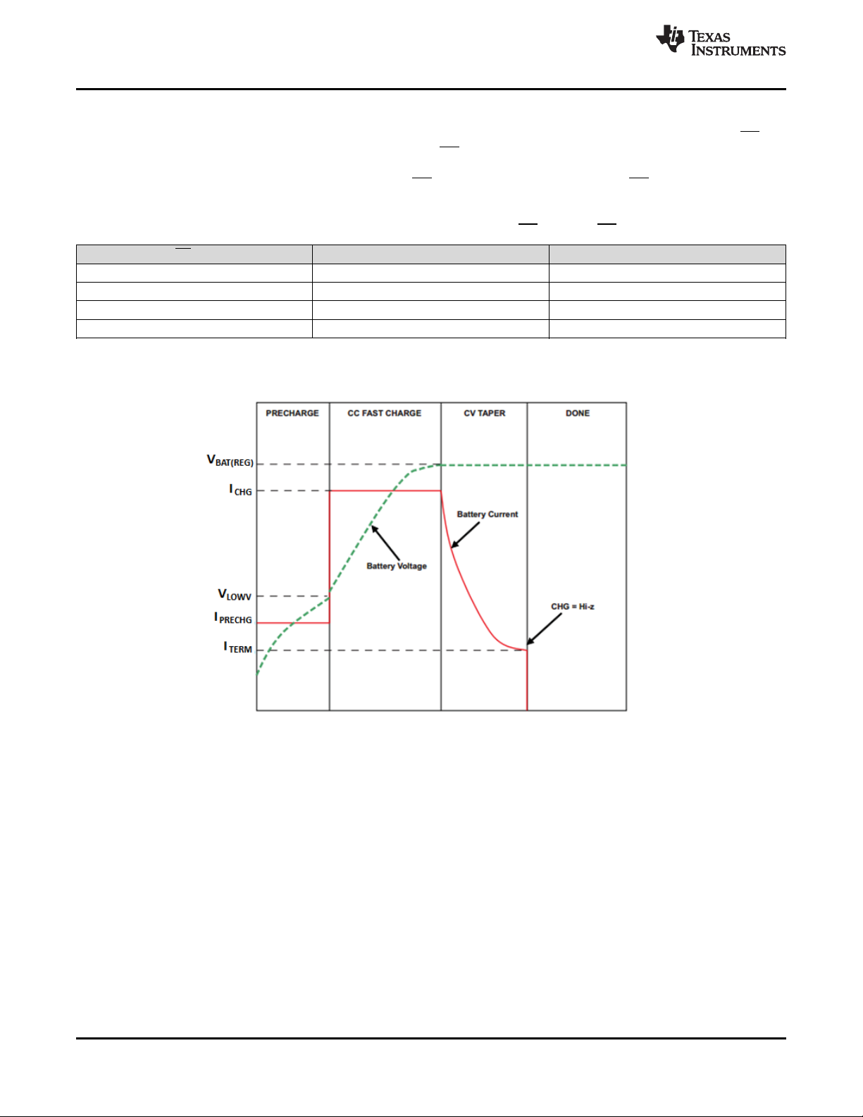
Figure 17. BQ21061 Typical Charge Cycle
During Pre-Charge, where the battery voltage is below the V
level, the battery willl be charge with I
LOWV
PRECHARGE
current which can be programmed through I2C. During pre-charge, the safety timer is set to 25% of the safety
timer value during fast charge. Once the battery voltage reaches V
Charge Mode, charging the battery at I
voltage approaches the V
BATREG
level, the charging current starts tapering off as shown in Figure 17. Once the
CHARGE
charging current reaches the termination current (I
is charged to V
BATREG
level, the regulated PMID voltage should be set to at least 200mV above V
which may also be programmed through I2C. Once the battery
) charging is stopped. Note that to ensure that the battery
TERM
, the charger will then operate in Fast
LOWV
BATREG
Termination is only enabled when the charger CV loop is active in fast charge operation. No termination will
occur if the charge current reaches I
while VINDPM or DPPM is active as well as the thermal regulation
TERM
loop. Termination is also disabled when operating in the TS WARM region. The charger only goes to termination
when the current drops to I
due to the battery reaching the target voltage and not due to the charge current
TERM
limitation imposed by the previously mentioned control loops
Whenever a change in the charge current setting is triggered, whether it occurs due to I2C programming by the
host, Pre-Charge/Fast Charge transition or JEITA TS control, the device will temporarily disable charging (for ~ 1
ms) before updating the charge current value.
14
Submit Documentation Feedback Copyright © 2019, Texas Instruments Incorporated
Product Folder Links: BQ21061
.
Page 15

BQ21061
www.ti.com
SLUSDU0 –SEPTEMBER 2019
7.3.1.2 JEITA and Battery Temperature Dependent Charging
The charger can be configured through I2C setting to provide JEITA support, automatically reducing the charging
current and voltage depending on the battery temperature as monitored by an NTC thermistor connected to the
BQ21061 TS pin. See External NTC Monitoring (TS) section for details.
7.3.1.3 Input Voltage Based Dynamic Power Management (VINDPM) and Dynamic Power Path Management (DPPM)
The VINDPM loop prevents the input voltage from collapsing to a point where charging would be interrupted by
reducing the current drawn by charger in order to keep VINfrom dropping below V
drops to V
, the VINDPM loops will reduce the input current through the blocking FETs, to prevent the
IN_DPM
. Once the IN voltage
IN_DPM
further drop of the supply voltage. The VINDPM function is disabled by default and may be enabled through I2C
command. The V
IN_DPM
On the other hand, the DPPM loop prevents the system output (PMID) from dropping below V
threshold is programmable through the I2C register from 4.2 V to 4.9 V in 100-mV steps.
+ 200mV when
BAT
the sum of the charge current and system load exceeds the BQ21061 input current limit setting. If PMID drops
below the DPPM voltage threshold, the charging current is reduced. If PMID continues to drop after BATFET
charging current is reduced to zero, the part will enter supplement mode when PMID falls below the supplement
mode threshold (V
BAT
- V
). NOte that DPPM function is disabled when PMID regulation is set to battery
BSUP1
tracking.
When the device enters these modes, the charge current may be lower than the set value and the corresponding
status bits and flags are set. If the 2X timer is set, the safety timer is extended while the loops are active.
Additionally, termination is disabled.
7.3.1.4 Battery Supplement Mode
When the PMID voltage drops below the battery voltage by V
, the battery supplements the system load.
BSUP1
The battery stops supplementing the system load when the voltage on the PMID pin rises above the battery
voltage by V
. During supplement mode, the battery supplement current is not regulated, however, the
BSUP2
Battery Over-Current Protection mechanism is active. Battery charge termination is disabled while in supplement
mode.
7.3.2 Protection Mechanisms
7.3.2.1 Input Over-Voltage Protection
The input over-voltage protection protects the device and downstream components connected to PMID, and BAT
against damage from over-voltage on the input supply. When VIN> V
an OVP fault is determined to exist.
OVP
During the OVP fault, the device turns the input FET off, sends a single 128-µs pulse on INT, and the
VIN_OVP_FAULT FLAG and STAT bits are updated over I2C. Once the OVP fault is removed, the STAT bit is
cleared and the device returns to normal operation. The FLAG bit is not cleared until it is read through I2C after
the OVP condition no longer exists. The OVP threshold for the device is 5.5 V to allow operation from standard
USB sources.
7.3.2.2 Safety Timer and I2C Watchdog Timer
At the beginning of the charge cycle, the device starts the safety timer. If charging has not terminated before the
programmed safety time, t
t
MAXCHG
. When a safety timer fault occurs, a single 128-µs pulse is sent on the INT pin and the
MAXCHG
, expires, charging is disabled. The pre-charge safety time, t
PRECHG
, is 25% of
SAFETY_TMR_FAULT_FLAG bit in the FLAG3 register is updated over I2C. The CE pin or input power must be
toggled in order to reset the safety timer and exit the fault condition. Note that the flag bit will be reset when the
bit is read by the host even if the fault has not been cleared. The safety timer duration is programmable using the
SAFETY_TIMER bits. When the safety timer is active, changing the safety timer duration resets the safety timer.
The device also contains a 2X_TIMER bit that doubles the timer duration prevent premature safety timer
expiration when the charge current is reduced by a high load on PMID (DPPM operation), VIN DPM, thermal
regulation, or a NTC (JEITA) condition. When 2X_TIMER function is enabled, the timer is allowed to run at half
speed when any loop is active other than CC or CV.
In addition, the BQ21061 has a 50s watchdog timer which resets after every I2C transaction. This feature, which
is enabled by default, resets all charger parameters registers to their default values when the timer expires.
Product Folder Links: BQ21061
Submit Documentation FeedbackCopyright © 2019, Texas Instruments Incorporated
15
Page 16

J A JA DISS
T T P
T
u
BQ21061
SLUSDU0 –SEPTEMBER 2019
www.ti.com
7.3.2.3 Thermal Protection and Thermal Charge Current Foldback
In order to protect the device from damage due to overheating, the junction temperature of the die, TJ, is
monitored. When TJreaches T
operation when TJfalls below T
SHUTDOWN
SHUTDOWN
During the charging process, the device will reduce the charging current at a rate of (0.04 x I
exceeds the thermal foldback threshold, T
the device stops operation and is turned off. The device resumes
by T
REG
.
HYS
CHARGE
)/°C once T
to prevent further heating. If the charge current is reduced to 0, the
battery supplies the current needed to supply the PMID output. The thermal regulation threshold may be set
through I2C by setting the THERM_REG bits to the desired value.
The die junction temperature, TJ, can be estimated based on the expected board performance using Equation 1:
(1)
Where P
is the total power dissipation in the IC. The θJAis largely driven by the board layout. For more
DISS
information about traditional and new thermal metrics, see the Semiconductor and IC Package Thermal Metrics
Application Report. Under typical conditions, the time spent in this state is very short.
7.3.2.4 Battery Short and Over Current Protection
In order to protect the device from over current and prevent excessive battery discharge current, the BQ21061
detects if the current on the battery FET exceeds I
(t
DGL_OCP
t
REC_SC
), the battery discharge FET is turned off and start operating in hiccup mode, re-enabling the BATFET
(250 ms) after being turned off by the over-current condition. If the over-current condition is triggered
BAT_OCP
. If the short circuit limit is reached for the deglitch time
upon retry for 3 to 7 consecutive times, the BATFET will then remain off until the part is reset or until Vin is
connected and valid. If the over-current condition and hiccup operation occurs while in supplement mode where
VIN is already present, VIN must be toggled in order for BATFET to be enabled and start another detection
cycle.
In the case where the battery is suddenly shorted while charging and VBAT drops below V
comparator quickly reduces the charge current to I
PRECHARGE
preventing fast charge current to be momentarily
SHORT
, a fast
injected to the battery while shorted.
J
7.3.2.5 PMID Short Circuit
A short on the PMID pin is detected when the PMID voltage drops below 1.6 V (PMID short threshold). PMID
short threshold has a 200-mV hysteresis. When this occurs, the input FET temporarily disconnects IN for up to
200 µs to prevent stress on the device if a sudden short condition happens, before allowing a softstart on the
PMID output.
7.3.3 VDD LDO
The device integrates a low current always-on LDO that serves as the digital I/O supply to the device. This LDO
is supplied by VIN or by BAT. The VDD LDO will remain on through all power states with the exception of Ship
Mode.
7.3.4 Load Switch/LDO Output and Control
The device integrates a low Iq load switch which can also be used as a regulated output. The LDO/LS has a
dedicated input pin VINLS and can support up to 150 mA of load current.
The LS/LDO may be enabled/disabled through I2C. The output voltage is programmable using the LS_LDO bits
in the registers. To limit voltage drop or voltage transients, a small ceramic capacitor must be placed close to
VINLS pin. Due to the body diode of the PMOS switch, it is recommended to have the capacitor on VINLS ten
times larger than the output capacitor on LS/LDO output.
Table 2. LDO Mode Control
I2C EN_LS_LDO LS_CONFIG LS/LDO OUTPUT
0 0 Pulldown
0 1 Pulldown
1 0 LDO
16
Submit Documentation Feedback Copyright © 2019, Texas Instruments Incorporated
Product Folder Links: BQ21061
Page 17

BQ21061
www.ti.com
SLUSDU0 –SEPTEMBER 2019
Table 2. LDO Mode Control (continued)
I2C EN_LS_LDO LS_CONFIG LS/LDO OUTPUT
1 1 Load Switch
The current capability of the LDO will depend on the VINLS input voltage and the programmed output voltage.
When the LS/LDO output is disabled through the register, an internal pull-down will discharge the output. The
LDO has output current limit protection, limiting the output current in the event of a short in the output. When the
LDO output current limit trips and is active for at least 1 ms, the device will set a flag and send an interrupt to the
host. The host must take action to disable the LDO if desired. The LDO may be set to operate as a load switch
by setting the LS_SWITCH_CONFG bit. Note that in order to change the configuration the LDO must be disabled
first, then the LS_SWITCH_CONFG bit is set for it to take effect.
7.3.5 PMID Power Control
The BQ21061 offers the option to control PMID through the I2C PMID_MODE bits. These bits can force PMID to
be supplied by BAT instead of IN, even if VIN> V
BAT
+ V
. They can also disconnect PMID, pulling it down or
SLP
leaving it floating. SeeTable 30 for details.
7.3.6 System Voltage (PMID) Regulation
The BQ21061 has a regulated system voltage output (PMID) that is programmable through I2C. PMID regulation
is only active when the adapter is connected and VIN> V
UVLO
, VIN> V
BAT
_ V
and VIN< V
SLP
. In Battery
OVP
Tracking operation (PMID_REG_CTRL = 000), the PMID voltage will be regulated to about 4.7% over battery
level (V
be at least 200mV higher than V
PMID
= V
x 1.047) or 3.8 V, whichever is higher. Note that the PMID regulation target should be set to
BAT
BATREG
.
7.3.7 MR Wake and Reset Input
The MR input has three main functions in the BQ21061. First, it serves as a means to wake the device from Ship
Mode. Second, it serves as a short button press detector, sending an interrupt to the host when the button
driving the MR pin has been pressed for a given period of time. This allows the implementation of different
functions in the end application such as menu selection and control. And finally it serves as a mean to get the
BQ21061 to reset the system by performing a power cycle (shut down PMID and automatically powering it back
on) or go to Ship Mode after detecting a long button press. The timing for the short and long button press
duration is programmable through I2C for added flexibility. Note that if a specific timer duration is changed
through I2C while that timer is active and has not expired, the new programmed value will be ignored until the
timer expires and/or is reset by MR. The MR input has an internal pull-up to BAT.
7.3.7.1 MR Wake or Short Button Press Functions
There are two programmable wake or short button press timers, WAKE1 and WAKE2. When the MR pin is held
low for t
WAKE1
the device sends an interrupt (128 µs active low pulse in the INT pin) and sets the
MRWAKE1_TIMEOUT flag when it expires. If the MR pin continues to be driven low after WAKE1 and the
WAKE2 timer expires, the BQ21061 sends a second interrupt and sets the MRWAKE2_TIMOUT flag. WAKE1 is
used as the timer to wake the device from ship mode. WAKE2’s only function is to send the interrupt and has no
effect on other BQ21061 functions. These flags are not cleared until they have been read by the host. Note that
interrupts are only sent when the flags are set and the flags must be cleared in order for another interrupt to be
sent upon MR press. The timer durations can be set through the MR_WAKEx_TIMER bits in the MRCTRL
Register section.
One of the main MR functions is to wake the device from Ship Mode when the MR is asserted. The device will
exit the Ship Mode when the MR pin is held low for at least t
. Immediately after the MR is asserted, VDD
WAKE1
will be enabled and the digital will start the WAKE counter. If the MR signal remains low until after the WAKE1
timer expires, the device will power up PMID and LDO (If enabled) completing the exit from the ship mode. If the
MR signal goes high before the WAKE1 timer expires, the device will go back to the Ship Mode operation, never
powering up PMID or the LDO. Note that if the MR pin remains low after exiting Ship Mode the wake interrupts
will not be sent and the long button press functions like HW reset will not occur until the MR pin is toggled. In the
case where a valid VIN(VIN> V
) is connected prior to WAKE2 timer expiring, the device will exit the ship
UVLO
mode immediately regardless of the MR or wake timer state. Figure 18 and Figure 19 show these different
scenarios.
Product Folder Links: BQ21061
Submit Documentation FeedbackCopyright © 2019, Texas Instruments Incorporated
17
Page 18
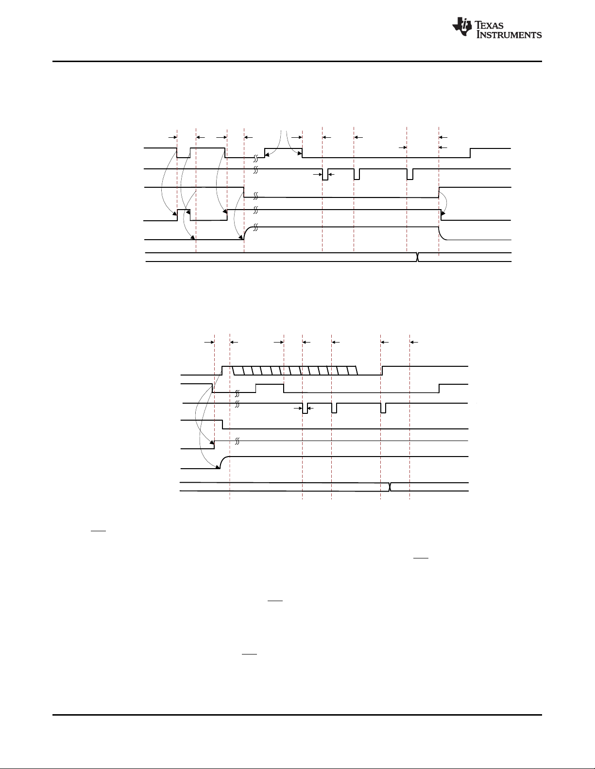
/MR
INT
SHIPMODE
VDD
twake1
twake2
treset_warn
thwreset
128us
twake1
Output Rails
(PMID, LDO if enabled)
VIN
MR_LPRESS_ACTION
Go to Ship Mode
'RQ¶WFDUH
twake1
twake2
thwreset
128us
twake1
No WAKE interrupts
are sent or reset
actions are taken
until /MR is toggled
after Ship Mode exit
Go to Ship Mode
/MR
INT
SHIPMODE
VDD
Output Rails
(PMID, LDO if enabled)
MR_LPRESS_ACTION 'RQ¶WFDUH
twake1
Thwreset_warn
BQ21061
SLUSDU0 –SEPTEMBER 2019
Figure 18. MR Wake from Ship Mode (MR_LPRESS_ACTION = Ship Mode, VIN not valid)
www.ti.com
Figure 19. MR Wake from Ship Mode – VIN Dependencies
7.3.7.2 MR Reset or Long Button Press Functions
The BQ21061 device may be configured to perform a system hardware reset (Power Cycle/Autowake), go into
Ship Mode, or simply do nothing after a long button press (for example, when the MR pin is driven low until the
MR_HW_RESET timer expires).The action taken by the device when the timer expires is configured through the
MR_LPRESS_ACTION bits in the ICCTRL1 Register section. Once the MR_HW_RESET timer expires the
device immediately performs the operation set by the MR_LPRESS_ACTION bits. The BQ21061 sends an
interrupt to the host when the device detects that MR has been pressed for a period that is within t
from reaching t
which would trigger a HW Reset or used as another button press timer interrupt like the WAKE1 and WAKE2
timers. This interrupt is sent before the MR_HW_RESET timer expires and sets the MRRESET_WARN flag. The
t
HW_RESET_WARN
change the reset behavior at any time after MR going low and prior to the MR_HW_RESET timer expiring. It may
not change it however from another behavior to a HW reset (Power Cycle/Autowake) since a HW reset can be
gated by other condition requirements, such as VIN presence (controlled by MR_RESET_VIN bit), throughout the
whole duration of the button press. This flexibility allows the host to abort any reset or power shutdown to the
system by overriding a long button press command.
18
Submit Documentation Feedback Copyright © 2019, Texas Instruments Incorporated
HW_RESET
. This may warn the host that the button has been pressed for a period close to t
may be set through I2C by the MR_RESET_WARN bits in the MRCTRL register. The host may
HW_RESET_WARN
HW_RESET
Product Folder Links: BQ21061
Page 19
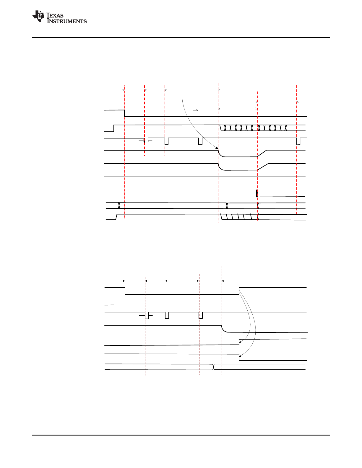
/MR
INT
SHIPMODE
VDD
twake1
twake2
Treset_warn
thwreset
128us
PMID & LDO
Shipmode enabled when both
MR has gone high and
thwreset has expired
VIN
MR_RESET_VIN has no effect
on this mode
MR_LPRESS_ACTION
'RQ¶WFDUH
Go to Shipmode
/MR
INT
PMID
LDO
VDD
SW reset
twake1
twake2
treset_
warn
thwreset
t_restart
128us
twake1
VIN
Once thwreset timer
expires and decision to
power cycle is done,
the device will always
complete the wake
after t_restart, no
matter change in VIN,
or bit control
MR_LPRESS_ACTION
'RQ¶WFDUH
00 - PowerCycle (AutoWake)
MR_RESET_VIN
Default
Default
BQ21061
www.ti.com
SLUSDU0 –SEPTEMBER 2019
A HW reset may also be started by setting the HW_RESET bit. Note that during a HW reset , VDD remains on.
Figure 21. MR Wake and Reset Timing Active Mode When MR_LPRESS_ACTION = 1x (Ship Mode) and
Figure 20. MR Wake and Reset Timing with VIN Present or BAT Active Mode When
MR_LPRESS_ACTION = 00
Only BAT is Present
Submit Documentation FeedbackCopyright © 2019, Texas Instruments Incorporated
Product Folder Links: BQ21061
19
Page 20

R/W
VIN
SHIPMODE
VDD
I2C
HWRESET_14S_WD
PMID
14s 14s
R/W
14s
R/W
HW Reset due to no I2C
transaction after VIN
detected
No HW Reset since
function was not reenabled after boot up
No HW Reset since I2C
transaction occurred
within 14s window of
VIN detection
BQ21061
SLUSDU0 –SEPTEMBER 2019
www.ti.com
7.3.8 14-Second Watchdog for HW Reset
The BQ21061 integrates a 14-second watchdog timer that makes the BQ21061 perform a HW reset/power cycle
if no I2C transaction is detected within 14 seconds of a valid adapter being connected. If the adapter is connected
and the host responds with an I2C transaction before the 14-second watchdog window expires, the part
continues in normal operation. The 14-second watchdog is disabled by default and may be enabled through I2C
by setting the HWRESET_14S_WD bit. Figure 22 shows the basic functionality of this feature.
Figure 22. 14-Second Watchdog for HW Reset Behavior
7.3.9 Faults Conditions and Interrupts (INT)
The device contains an open-drain output that signals an interrupt and is valid only after the device has
completed start-up into a valid state. If the part starts into a fault, interrupts will not be sent. The INT pin is
normally in high impedance and is pulled low for 128 µs when an interrupt condition occurs. When a fault or
status change occurs or any other condition that generates an interrupt such as CHARGE_DONE, a 128-µs
pulse (interrupt) is sent on INT to notify the host. All interrupts may be masked through I2C. If the interrupt
condition occurs while the interrupt is masked an interrupt pulse will not be sent. If the interrupt is unmasked
while the fault condition is still present, an interrupt pulse will not be sent until the INT trigger condition occurs
while unmasked.
7.3.9.1 Flags and Fault Condition Response
Table 3 below details the BQ21061 behavior when a fault condition occurs.
Table 3. Interrupt Triggers and Fault Condition Response
INTERRUPT
FAULT / FLAG DESCRIPTION
Set when charger
CHRG_CV_FLAG
enters Constant
Voltage operation
CHARGE_DONE_FLAGSet when charger
reaches termination
IINLIM_ACTIVE_FLA
G
Set when Input
Current Limit loop is
active
VDPPM_ACTIVE_FLAGSet when DPPM loop
is active
VINDPM_ACTIVE_FLAGSet when VINDPM
20
Submit Documentation Feedback Copyright © 2019, Texas Instruments Incorporated
loop is active
TRIGGER
BASED ON
STATUS BIT
CHANGE
Rising Edge Enabled No effect
Rising Edge
Rising Edge
Rising Edge
Rising Edge
Product Folder Links: BQ21061
CHARGER
BEHAVIOR
Paused- Charging
resumes with VIN or
CE toggle or when
V
is reached
RCH
Enabled. Reduced
charge current.
Enabled. Reduced
charge current.
Enabled. Reduced
charge current.
CHARGER SAFETY
TIMER
Reset
Doubled if option is
enabled
Doubled if option is
enabled
Doubled if option is
enabled
PMID BEHAVIOR
IN powered if VINis
valid
IN powered if VINis
valid
IN powered VIN
powered unless
supplement mode
condition is met.
VIN powered unless
supplement mode
condition is met.
VIN powered unless
supplement mode
condition is met.
Page 21

www.ti.com
Table 3. Interrupt Triggers and Fault Condition Response (continued)
FAULT / FLAG DESCRIPTION
Set when Thermal
THERMREG_ACTIVE
VIN_PGOOD_FLAG
VIN_OVP_FAULT_FL
AG
BAT_OCP_FAULT_F
LAG
BAT_UVLO_FAULT_
FLAG
TS_COLD_FLAG
TS_COOL_FLAG
TS_WARM_FLAG
TS_HOT_FLAG Set when VTS< V
TS_OPEN_FLAG
WD_FAULT_FLAG
SAFETY_TMR_FAUL
T_FLAG
LS_LDO_OCP_FAUL
T_FLAG
MRWAKE1_TIMEOU
T_FLAG
MRWAKE2_TIMEOU
T_FLAG
MRRESET_WARN_F
LAG
TSHUT
Charge Current
Foldback (Thermal
Regulation) loop is
Set when VIN
changes PGOOD
Set when VIN> V
Set when I
I
Set when V
V
Set when VTS>
V
Set when V
VTS> V
Set when V
VTS< V
Set when VTS>
V
Set when I2C
watchdog timer
expires
Set when safety Timer
expires. Cleared after
VIN or CE toggle
Set when LDO output
current exceeds OCP
condition
Set when MR is low
for at least t
Set when MR is low
for at least t
Set when MR is low
for at least
t
RESETWARN
No flag. Die
temperature exceeds
thermal shutdown
threshold is reached
active
status
BATOCP
BATUVLO
TS_COLD
TS_COLD
TS_COOL
TS_HOT
TS_WARM
TS_OPEN
BAT
BAT
WAKE1
WAKE2
INTERRUPT
STATUS BIT
Rising and Falling
OVP
>
<
>
<
HOT
BQ21061
SLUSDU0 –SEPTEMBER 2019
TRIGGER
BASED ON
CHANGE
Rising Edge
Edge
Rising Edge
Rising Edge
Rising Edge Enabled No effect
Rising Edge
Rising Edge
Rising Edge
Rising Edge
Rising Edge
Rising Edge Enabled N/A N/A
Rising Edge
Rising Edge N/A N/A N/A
Rising Edge N/A N/A N/A
Rising Edge N/A N/A N/A
Rising Edge N/A N/A N/A
N/A Disabled Disabled Disabled
CHARGER
BEHAVIOR
Enabled. Reduced
charge current.
If VIN_PGOOD_STAT
is low, charging is
disabled.
Charging is paused
until condition
disappears
Disabled (BAT only
condition)
Charging paused until
condition is cleared
Enabled. Reduced
charge current.
Enabled. Reduce
battery regulation
voltage.
Charging paused until
condition is cleared
Charging is paused
until condition
disappears
Disabled until VIN or
CE toggle
CHARGER SAFETY
TIMER
Doubled if option is
enabled
Reset
Reset BAT powered
N/A Disconnect BAT
Paused
Doubled if option is
enabled
No effect
Paused
Paused N/A
Reset after flag is
cleared
PMID BEHAVIOR
VIN powered unless
supplement mode
condition is met.
VIN powered (if
VIN_PGOOD_STAT
=1) unless
PMID_MODE is not
00.
IN powered of VINis
valid
IN powered of VINis
valid
IN powered of VINis
valid
IN powered of VINis
valid
IN powered of VINis
valid
IN powered of VINis
valid
7.3.10 Power Good (PG) Pin
The PG pin is an open-drain output that by default indicates when a valid IN supply is present. It may also be
configured to be a general purpose output (GPO) controlled through I2C or to be a level shifted version of the MR
input signal. Connect PG to the desired logic voltage rail using a 1-kΩ to 100-kΩ resistor, or use with an LED for
visual indication. See Table 30 for details
Submit Documentation FeedbackCopyright © 2019, Texas Instruments Incorporated
Product Folder Links: BQ21061
21
Page 22

BQ21061
TS
VDD
NTC R
PARALLEL
R
PARALLEL
= R
NTC@25C
TS I
BIAS
+
_
+
_
+
_
+
_
TS_HOT
TS_WARM
TS_COOL
TS_COLD
Disable Charge
Disable Charge
Reduce I
CHARGE
Reduce V
O_REG
BQ21061
SLUSDU0 –SEPTEMBER 2019
www.ti.com
7.3.11 External NTC Monitoring (TS)
The I2C interface allows the user to easily implement the JEITA standard for systems where the battery pack
thermistor is monitored by the host. Additionally, the device provides a flexible voltage based TS input for
monitoring the battery pack NTC thermistor. The voltage at TS is monitored to determine that the battery is at a
safe temperature during charging.
The part can be configured to meet JEITA requirements or a simpler HOT/COLD function only. Additionally, the
TS charger control function can be disabled. To satisfy the JEITA requirements, four temperature thresholds are
monitored: the cold battery threshold, the cool battery threshold, the warm battery threshold, and the hot battery
threshold. These temperatures correspond to the V
Characteristics table. Charging and safety timers are suspended when VTS< V
VTS< V
, the charging current is reduced to the value programmed in the TS_FASTCHGCTRL register. Note
COLD
COLD
, V
COOL
, V
WARM
, and V
HOT
thresholds in the Electrical
HOT
or VTS> V
COLD
. When V
COOL
that the current steps for fast charge in the COOL region, just as those in normal fast charge, are multiples of the
fast charge LSB value (1.25 mA by default). So in the case where the calculated scaled down current for the
COOL region falls in between charge current steps, the device will round down the charge current to the nearest
step. For example, if the fast charge current is set for 15 mA (ICHG = 1100) and TS_FASTCHARGE =111
(0.125*ICHG), the charge current in the COOL region will be 1.25 mA instead of the calculated 1.85 mA.
When V
< VTS< V
HOT
, the battery regulation voltage is reduced to the value programmed in the
WARM
TS_FASTCHGCTRL register.
Regardless of whether the part is configured for JEITA, HOT/COLD, or disabled, when a TS fault occurs, a 128µs pulse is sent on the INT output, and the FAULT bits of the register are updated over I2C. The FAULT bits are
not cleared until they are read over I2C. This allows the host processor to take action if a different behavior than
the pre-set function is needed. Alternately, the TS pin voltage can be read by the host if VIN is present or when
BAT is present, so the appropriate action can be taken by the host.
<
7.3.11.1 TS Thresholds
The BQ21061 monitors the TS voltage and sends an interrupt to the host whenever it crosses the V
V
COOL
and V
thresholds which correspond to different temperature thresholds based on the NTC resistance
COLD
HOT
, V
WARM
and biasing. These thresholds may be adjusted through I2C by the host. The device will also disable charging if
TS pin exceeds the V
TS_OPEN
The TS biasing circuit is shown in Figure 23. Note that the respective VTSfor T
(45°C) and T
(60°C) changes for every NTC, therefore the threshold values may need to be adjusted through
HOT
threshold.
COLD
(0°C), T
COOL
(10°C), T
WARM
I2C based on the supported NTC type.
,
The BQ21061 supports by default the following thresholds for a 10-KΩ NTC.
22
Submit Documentation Feedback Copyright © 2019, Texas Instruments Incorporated
Figure 23. TS Bias Functional Diagram
Product Folder Links: BQ21061
Page 23

START Condition
DATA
CLK
STOP Condition
S
P
BQ21061
www.ti.com
SLUSDU0 –SEPTEMBER 2019
Table 4. TS Thresholds for 10-KΩ Thermistor with 3380 B-Constant
THRESHOLD
Open -- >0.9
Cold 0 0.585
Cool 10 0.514
Warm 45 0.265
Hot 60 0.185
TEMPERATURE
(°C)
VTS (V)
7.3.12 I2C Interface
The BQ21061 device uses a fully compliant I2C interface to program and read control parameters, status bits,
and so on. I2C is a 2-wire serial interface developed by Philips Semiconductor (see I2C-Bus Specification,
Version 2.1, January 2000). The bus consists of a data line (SDA) and a clock line (SCL) with pull-up structures.
When the bus is idle, both SDA and SCL lines are pulled high. All the I2C compatible devices connect to the I2C
bus through open drain I/O pins, SDA and SCL. A master device, usually a micro-controller or a digital signal
processor, controls the bus. The master is responsible for generating the SCL signal and device addresses. The
master also generates specific conditions that indicate the START and STOP of data transfer. A slave device
receives and/or transmits data on the bus under control of the master device.
The BQ21061 works as a slave and supports the following data transfer modes, as defined in the I2C Bus
Specification: standard mode (100 kbps) and fast mode (400 kbps). The interface adds flexibility to the battery
charge solution, enabling most functions to be programmed to new values depending on the instantaneous
application requirements.
Register contents remain intact as long as VBAT or VIN voltages remains above their respective UVLO levels.
The data transfer protocol for standard and fast modes is exactly the same; therefore, they are referred to as the
F/S-mode in this document. The BQ21061 device 7-bit address is 0×6B (shifted 8-bit address is 0xD6).
7.3.12.1 F/S Mode Protocol
The master initiates data transfer by generating a start condition. The start condition is when a high-to-low
transition occurs on the SDA line while SCL is high, as shown in Figure 24. All I2C-compatible devices should
recognize a start condition.
Figure 24. START and STOP Condition
The master then generates the SCL pulses, and transmits the 8-bit address and the read/write direction bit R/W
on the SDA line. During all transmissions, the master ensures that data is valid. A valid data condition requires
the SDA line to be stable during the entire high period of the clock pulse (see Figure 25). All devices recognize
the address sent by the master and compare it to their internal fixed addresses. Only the slave device with a
matching address generates an acknowledge (see Figure 26) by pulling the SDA line low during the entire high
period of the ninth SCL cycle. Upon detecting this acknowledge, the master knows that communication link with a
slave has been established.
Product Folder Links: BQ21061
Submit Documentation FeedbackCopyright © 2019, Texas Instruments Incorporated
23
Page 24

Data Output
by Transmitter
Data Output
by Receiver
SCL From
Master
Not Acknowledge
Acknowledge
Clock Pulse for
Acknowledgement
1 2
8
9
START
Condition
DATA
CLK
Data Line
Stable;
Data Valid
Change
of Data
Allowed
BQ21061
SLUSDU0 –SEPTEMBER 2019
www.ti.com
Figure 25. Bit Transfer on the Serial Interface
The master generates further SCL cycles to either transmit data to the slave (R/W bit 1) or receive data from the
slave (R/W bit 0). In either case, the receiver needs to acknowledge the data sent by the transmitter. So an
acknowledge signal can either be generated by the master or by the slave, depending on which one is the
receiver. The 9-bit valid data sequences consisting of 8-bit data and 1-bit acknowledge can continue as long as
necessary. To signal the end of the data transfer, the master generates a stop condition by pulling the SDA line
from low to high while the SCL line is high (see Figure 24). This releases the bus and stops the communication
link with the addressed slave. All I2C compatible devices must recognize the stop condition. Upon the receipt of a
stop condition, all devices know that the bus is released, and wait for a start condition followed by a matching
address. If a transaction is terminated prematurely, the master needs to send a STOP condition to prevent the
slave I2C logic from remaining in an incorrect state. Attempting to read data from register addresses not listed in
this section will result in FFh being read out.
24
Figure 26. Acknowledge on the I2C Bus
Submit Documentation Feedback Copyright © 2019, Texas Instruments Incorporated
Product Folder Links: BQ21061
Page 25

SDA
SCL
Recognize START or
REPEATED START
Condition
Recognize STOP or
REPEATED START
Condition
Generate ACKNOWLEDGE
Signal
Acknowledgement
Signal From Slave
MSB
Address
R/W
ACK
S
or
Sr
Sr
or
P
P
Sr
ACK
www.ti.com
BQ21061
SLUSDU0 –SEPTEMBER 2019
Figure 27. Bus Protocol
Product Folder Links: BQ21061
Submit Documentation FeedbackCopyright © 2019, Texas Instruments Incorporated
25
Page 26

BQ21061
SLUSDU0 –SEPTEMBER 2019
www.ti.com
7.4 Device Functional Modes
The BQ21061 has four main modes of operation: Active Battery Mode, Low Power Mode and Ship Mode which
are battery only modes and Charge/Adapter Mode when a supply is connected to IN. Table 5 below summarizes
the functions that are active for each operation mode. Each mode is discussed in further detail in the following
sections in addition to the device's power-up/down sequences.
Table 5. Function Availability Based on Primary Mode of Operation
FUNCTION
VOVP Yes No Yes Yes
VUVLO Yes Yes Yes Yes
BATOCP Yes No No Yes
BATUVLO Yes No Yes Yes
VINDPM If enabled No No No
DPPM If enabled No No No
VDD Yes No Yes Yes
LS/LDO Yes No If enabled If enabled
BATFET Yes No Yes Yes
TS Measurement Yes No No If enabled
Battery Changing If enabled No No No
ILIM Yes (Register Value) No No No
MR input Yes Yes Yes Yes
LP input No No Yes Yes
INT output Yes No No Yes
I2C Yes No No Yes
CE input Yes No No No
CHARGE/ ADAPTER
MODE
SHIP MODE
LOW POWER
MODE
ACTIVE BATTERY MODE
7.4.1 Ship Mode
Ship Mode is the lowest quiescent current state for the device. Ship Mode latches off the device and BAT FET
until VIN> V
or the MR button is depressed for t
UVLO
and released. Ship mode can be entered regardless of
WAKE1
the state of CE. The device will also enter Ship Mode upon battery insertion when no valid VIN is present. If the
EN_SHIPMODE is written to a 1 while a valid input supply is connected, the device will wait until the IN supply is
removed to enter ship mode. If the MR pin is held low when the EN_SHIPMODE bit is set, the device will wait
until the MR pin goes high before entering Ship Mode. Figure 28 shows this behavior. The battery voltage must
be above the maximum programmable V
BATUVLO
threshold in order to exit Ship Mode with MR press. The
EN_SHIPMODE bit can be cleared using the I2C interface as well while the VIN input is valid. The
EN_SHIPMODE bit is not cleared upon the I2C watchdog expiring, this means that if watchdog timer fault occurs
while the EN_SHIPMODE bit is set and the device is waiting to go into Ship Mode because VINis present or MR
is low, the device will still proceed to go into Ship Mode once those conditions are cleared.
26
Submit Documentation Feedback Copyright © 2019, Texas Instruments Incorporated
Product Folder Links: BQ21061
Page 27

VBAT
VIN
/MR
SHIPMODE
t
WAKE1
BQ21061
www.ti.com
SLUSDU0 –SEPTEMBER 2019
Figure 28. Ship Mode Entry Based On EN_SHIPMODE bit
7.4.2 Low Power
Low Power mode is a low quiescent current state while operating from the battery. The device will operate in low
power mode when the LP pin is set low, VIN< V
, MR pin is high and all I2C transactions and interrupts that
UVLO
started while in the Active Battery or Charging Modes have been completed and sent. During LP mode the VDD
output is powered by BAT, the MR inputs are active and the I2C is disabled. All other circuits, such as oscillators,
are in a low power or off state. The LS/LDO outputs will remain in the state set by the EN_LS_LDO bit prior to
entering Low Power Mode. The device exits LP Mode when the LP pin is set high or VIN> V
In the case that a faulty adapter with VIN> V
is connected to the device while LP pin is low, the device will be
OVP
UVLO
.
powered from the battery, but will operate in Active battery mode instead of Low Power mode regardless of the
LP pin state.
When MR is held low while LP is low, the device will enter Active Battery Mode, this allows for the internal clocks
of the device to be running and allow the MR long button press HW reset. I2C operation may also be possible
during this condition. Note that as soon as the MR input is released and goes high, the device will go back to LP
Mode tuning off all clocks. Note that if a HW reset has occurred while LP is low, MR must remain low until the
power cycle has completed (PMID and LDO enable) to allow completion of the power up sequence.
7.4.3 Active Battery
When the device is out of Ship Mode and battery is above V
BATUVLO
with no valid input source, the battery
discharge FET is turned on connecting PMID to the battery. The current flowing from BAT to PMID is not
regulated, but it is monitored by the battery over-current protection (OCP) circuitry. If the battery discharge
current exceed the OCP threshold, the battery discharge FET will be turned off as detailed in the Battery Short
and Over Current Protection section.
If only battery is connected and the battery voltage goes below V
BATUVLO
, the battery discharge FET is turned off.
To provide designers the most flexibility in optimizing their system, an adjustable BATUVLO is provided. Deeper
discharge of the battery enables longer times between charging, but may shorten the battery life. The BATUVLO
is adjustable with a fixed 150-mV hysteresis.
7.4.4 Charger/Adapter Mode
This mode is active when VIN> V
. If the supply at IN is valid and above the V
UVLO
IN_DPM
level, PMID will be
powered by the supply connected to IN. The device will charge the battery, if charging is enabled, until
termination has occurred.
7.4.5 Power-Up/Down Sequencing
The power-up and power-down sequences for the BQ21061 are shown below. Upon VINinsertion, VIN> V
the device wakes up, powering the VDD rail. If VIN> V
and if VIN> V
charging will start if enabled.
IN_DPM
Product Folder Links: BQ21061
BAT
+ V
and VIN< V
SLP
, PMID will be powered by VIN
OVP
Submit Documentation FeedbackCopyright © 2019, Texas Instruments Incorporated
UVLO
,
27
Page 28

VBAT
PMID
VDD
VIN
/MR
/MR Deglitch Delay
t
WAKE1
VIN
VBAT
VDD
IBAT
PMID
SHIPMODE
Charging
starts
V
BAT
<
V
BUVLO
Battery
supplies
power
Battery
insertion
VIN level
V
BAT
level
Digital wakes up
for shipmode
entry
Triggers shipmode exit. If
VBAT = VBATREG then
termination happen and no
charging occurs
BQ21061
SLUSDU0 –SEPTEMBER 2019
www.ti.com
In the case where VIN< V
and the battery is inserted (V
UVLO
BAT
> V
BATUVLO
), the device will immediately enter
Ship Mode unless MR is held low. Upon battery insertion the VDD rail will come up to allow the device to check
the MR state and if MR is high VDD will immediately be disabled and the device will enter Ship Mode. If MR is
low, the device will start the WAKE timer and power up PMID and other rails if MR is held low for longer than
t
.
WAKE1
Figure 29. BQ21061 Wake-Up Upon Supply Insertion
Figure 30. BQ21061 Wake-Up Upon Battery Insertion
28
Submit Documentation Feedback Copyright © 2019, Texas Instruments Incorporated
Product Folder Links: BQ21061
Page 29

BQ21061
www.ti.com
SLUSDU0 –SEPTEMBER 2019
7.5 Register Map
The device 7-bit address I2C is 0x6B (shifted 8-bit address is 0xD6).
7.5.1 I2C Registers
Table 6 lists the memory-mapped registers for the I2C registers. All register offset addresses not listed in Table 6
should be considered as reserved locations and the register contents should not be modified.
Table 6. I2C Registers
Address Acronym Register Name Section
0x0 STAT0 Charger Status 0 Go
0x1 STAT1 Charger Status 1 Go
0x2 STAT2 Status 2 Go
0x3 FLAG0 Charger Flags 0 Go
0x4 FLAG1 Charger Flags 1 Go
0x5 FLAG2 Flags 2 Go
0x6 FLAG3 Timer Flags Go
0x7 MASK0 Interrupt Masks 0 Go
0x8 MASK1 Interrupt Masks 1 Go
0x9 MASK2 Interrupt Masks 2 Go
0xA MASK3 Interrupt Masks 3 Go
0x12 VBAT_CTRL Battery Voltage Control Go
0x13 ICHG_CTRL Fast Charge Current Control Go
0x14 PCHRGCTRL Pre-Charge Current Control Go
0x15 TERMCTRL Termination Current Control Go
0x16 BUVLO Battery UVLO and Current Limit Control Go
0x17 CHARGERCTRL0 Charger Control 0 Go
0x18 CHARGERCTRL1 Charger Control 1 Go
0x19 ILIMCTRL Input Corrent Limit Control Go
0x1D LDOCTRL LDO Control Go
0x30 MRCTRL MR Control Go
0x35 ICCTRL0 IC Control 0 Go
0x36 ICCTRL1 IC Control 1 Go
0x37 ICCTRL2 IC Control 2 Go
0x61 TS_FASTCHGCTRL TS Charge Control Go
0x62 TS_COLD TS Cold Threshold Go
0x63 TS_COOL TS Cool Threshold Go
0x64 TS_WARM TS Warm Threshold Go
0x65 TS_HOT TS Hot Threshold Go
0x6F DEVICE_ID Device ID Go
Complex bit access types are encoded to fit into small table cells. Table 7 shows the codes that are used for
access types in this section.
Table 7. I2C Access Type Codes
Access Type Code Description
Read Type
R R Read
RC C
R
Write Type
W W Write
Product Folder Links: BQ21061
to Clear
Read
Submit Documentation FeedbackCopyright © 2019, Texas Instruments Incorporated
29
Page 30

BQ21061
SLUSDU0 –SEPTEMBER 2019
Table 7. I2C Access Type Codes (continued)
Access Type Code Description
Reset or Default Value
-n Value after reset or the default
value
7.5.1.1 STAT0 Register (Address = 0x0) [reset = X]
STAT0 is shown in Figure 31 and described in Table 8.
Return to Summary Table.
Figure 31. STAT0 Register
7 6 5 4 3 2 1 0
RESERVED CHRG_CV_STATCHARGE_DON
E_STAT
R-X R-X R-X R-X R-X R-X R-X R-X
IINLIM_ACTIVE
_STAT
VDPPM_ACTIV
E_STAT
VINDPM_ACTI
VE_STAT
THERMREG_A
CTIVE_STAT
Table 8. STAT0 Register Field Descriptions
Bit Field Type Reset Description
7 RESERVED R X Reserved
6 CHRG_CV_STAT R X Constant Voltage Charging Mode (Taper Mode) Status
1b0 = Not Active
1b1 = Active
5 CHARGE_DONE_STAT R X Charge Done Status
1b0 = Not Active
1b1 = Active
4 IINLIM_ACTIVE_STAT R X Input Current Limit Status
1b0 = Not Active
1b1 = Active
3 VDPPM_ACTIVE_STAT R X DPPM Status
1b0 = Not Active
1b1 = Active
2 VINDPM_ACTIVE_STAT R X VINDPM Status
1b0 = Not Active
1b1 = Active
1 THERMREG_ACTIVE_STATR X Thermal Regulation Status
1b0 = Not Active
1b1 = Active
0 VIN_PGOOD_STAT R X VIN Power Good Status .
1b0 = Not Good
1b1 = VIN> V
UVLO
and VIN> V
BAT
+ V
and VIN< V
SLP
www.ti.com
VIN_PGOOD_
STAT
OVP
7.5.1.2 STAT1 Register (Address = 0x1) [reset = X]
STAT1 is shown in Figure 32 and described in Table 9.
Return to Summary Table.
Figure 32. STAT1 Register
7 6 5 4 3 2 1 0
VIN_OVP_FAU
LT_STAT
R-X R-X R-X R-X R-X R-X R-X R-X
30
Submit Documentation Feedback Copyright © 2019, Texas Instruments Incorporated
RESERVED BAT_OCP_FA
ULT_STAT
BAT_UVLO_FA
ULT_STAT
Product Folder Links: BQ21061
TS_COLD_STATTS_COOL_STATTS_WARM_STATTS_HOT_STAT
Page 31

www.ti.com
Table 9. STAT1 Register Field Descriptions
Bit Field Type Reset Description
7 VIN_OVP_FAULT_STAT R X VIN Overvoltage Status
1b0 = Not Active
1b1 = Active
6 RESERVED R X Reserved
5 BAT_OCP_FAULT_STAT R X Battery Over-Current Protection Status
1b0 = Not Active
1b1 = Active
4 BAT_UVLO_FAULT_STATR X Battery voltage below BATUVLO Level Status
1b0 = V
1b1 = V
3 TS_COLD_STAT R X TS Cold Status - VTS> V
1b0 = Not Active
1b1 = Active
2 TS_COOL_STAT R X TS Cool Status - V
value set by TS_Registers)
1b0 = Not Active
1b1 = Active
1 TS_WARM_STAT R X TS Warm - V
set by TS_Registers)
1b0 = Not Active
1b1 = Active
0 TS_HOT_STAT R X TS Hot Status - VTS< V
1b0 = Not Active
1b1 = Active
BAT
BAT
> V
< V
WARM
BATUVLO
BATUVLO
COOL
> VTS>V
(charging suspended)
COLD
< VTS< V
HOT
(charging suspended)
HOT
BQ21061
SLUSDU0 –SEPTEMBER 2019
(charging current reduced by
COLD
(charging voltage reduced by value
7.5.1.3 STAT2 Register (Address = 0x2) [reset = X]
STAT2 is shown in Figure 33 and described in Table 10.
Return to Summary Table.
Figure 33. STAT2 Register
7 6 5 4 3 2 1 0
RESERVED TS_OPEN_ST
R-X R-X R-X R-X R-X R-X
Table 10. STAT2 Register Field Descriptions
Bit Field Type Reset Description
7-4 RESERVED R X Reserved
3-1 RESERVED R X Reserved
0 TS_OPEN_STAT R X TS Open Status
1b0 = VTS< V
1b1 = VTS> V
OPEN
OPEN
7.5.1.4 FLAG0 Register (Address = 0x3) [reset = 0x0]
FLAG0 is shown in Figure 34 and described in Table 11.
Return to Summary Table.
Clear on Read
AT
Product Folder Links: BQ21061
Submit Documentation FeedbackCopyright © 2019, Texas Instruments Incorporated
31
Page 32

BQ21061
SLUSDU0 –SEPTEMBER 2019
Figure 34. FLAG0 Register
7 6 5 4 3 2 1 0
RESERVED CHRG_CV_FLAGCHARGE_DON
E_FLAG
RC-1b0 RC-1b0 RC-1b0 RC-1b0 RC-1b0 RC-1b0 RC-1b0 RC-1b0
IINLIM_ACTIVE
_FLAG
VDPPM_ACTIV
E_FLAG
VINDPM_ACTI
VE_FLAG
THERMREG_A
CTIVE_FLAG
Table 11. FLAG0 Register Field Descriptions
Bit Field Type Reset Description
7 RESERVED RC 1b0 Reserved
6 CHRG_CV_FLAG RC 1b0 Constant Voltage Charging Mode (Taper Mode) Flag
1b0 = CV Mode Entry not detected
1b1 = CV Mode Entry detected
5 CHARGE_DONE_FLAG RC 1b0 Charge Done Flag
1b0 = Charge Done (Termination) not detected
1b1 = Charge Done (Termination) detected
4 IINLIM_ACTIVE_FLAG RC 1b0 Input Current Limit Flag
1b0 = Input Current Limit not detected
1b1 = Input Current Limit detected
3 VDPPM_ACTIVE_FLAG RC 1b0 DPPM Flag
1b0 = DPPM operation not detected
1b1 = DPPM operation detected
2 VINDPM_ACTIVE_FLAG RC 1b0 VINDPM Flag
1b0 = VINDPM operation not detected
1b1 = VIINDPM operation detected
1 THERMREG_ACTIVE_FLAGRC 1b0 Thermal Regulation Flag
1b0 = Thermal Regulation not detected
1b1 = Thermal Regulation detected
0 VIN_PGOOD_FLAG RC 1b0 VIN Power Good Flag . Interrupt will not be sent if device powers up
with VIN_PGOOD condition and V
1b0 = No change in VIN Power Good Status
1b1 = Change in VIN Power Good Status detected.
BAT
< V
BATUVLO
www.ti.com
VIN_PGOOD_F
LAG
7.5.1.5 FLAG1 Register (Address = 0x4) [reset = 0x0]
FLAG1 is shown in Figure 35 and described in Table 12.
Return to Summary Table.
Clear on Read
Figure 35. FLAG1 Register
7 6 5 4 3 2 1 0
VIN_OVP_FAU
LT_FLAG
RC-1b0 RC-1b0 RC-1b0 RC-1b0 RC-1b0 RC-1b0 RC-1b0 RC-1b0
RESERVED BAT_OCP_FA
ULT_FLAG
BAT_UVLO_FA
ULT_FLAG
TS_COLD_FLAGTS_COOL_FLAGTS_WARM_FLAGTS_HOT_FLAG
Table 12. FLAG1 Register Field Descriptions
Bit Field Type Reset Description
7 VIN_OVP_FAULT_FLAG RC 1b0 VIN Over Voltage Fault Flag
1b0 = No overvoltage condition detected
1b1 = VIN overvoltage condition detected
6 RESERVED RC 1b0 Reserved
32
Submit Documentation Feedback Copyright © 2019, Texas Instruments Incorporated
Product Folder Links: BQ21061
Page 33

www.ti.com
Table 12. FLAG1 Register Field Descriptions (continued)
Bit Field Type Reset Description
5 BAT_OCP_FAULT_FLAG RC 1b0 Battery Over Current Protection Flag
1b0 = No Battery Over Current condition detected
1b1 = Battery Over Current condition detected
4 BAT_UVLO_FAULT_FLAGRC 1b0 Battery Under Voltage Flag
1b0 = Battery below BATUVLO condition detected
1b1 = No Battery below BATUVLO condition detected
3 TS_COLD_FLAG RC 1b0 TS Cold Region Entry Flag
1b0 = TS Cold Region Entry not detected
1b1 = TS Cold Region Entry detected
2 TS_COOL_FLAG RC 1b0 TS Cool Region Entry Flag
1b0 = TS Cool Region Entry not detected
1b1 = TS Co0l Region Entry detected
1 TS_WARM_FLAG RC 1b0 TS Warm Region Entry Flag
1b0 = TS Warm Region Entry not detected
1b1 = TS Warm Region Entry detected
0 TS_HOT_FLAG RC 1b0 TS Hot Region Entry Flag
1b0 = TS Hot Region Entry not detected
1b1 = TS Hot Region Entry detected
BQ21061
SLUSDU0 –SEPTEMBER 2019
7.5.1.6 FLAG2 Register (Address = 0x5) [reset = 0x0]
FLAG2 is shown in Figure 36 and described in Table 13.
Return to Summary Table.
Clear on Read
Figure 36. FLAG2 Register
7 6 5 4 3 2 1 0
RESERVED TS_OPEN_FLA
RC-1b0 RC-1b0 RC-1b0 RC-1b0 RC-3b000 RC-1b0
Table 13. FLAG2 Register Field Descriptions
Bit Field Type Reset Description
7-4 RESERVED R X Reserved
3-1 RESERVED RC 3b000 Reserved
0 TS_OPEN_FLAG RC 1b0 TS Open Flag
1b0 = No TS Open fault detected
1b1 = TS Open fault detected
7.5.1.7 FLAG3 Register (Address = 0x6) [reset = 0x0]
FLAG3 is shown in Figure 37 and described in Table 14.
Return to Summary Table.
Clear on Read
G
Figure 37. FLAG3 Register
7 6 5 4 3 2 1 0
RESERVED WD_FAULT_FLAGSAFETY_TMR
_FAULT_FLAG
RC-1b0 RC-1b0 RC-1b0 RC-1b0 RC-1b0 RC-1b0 RC-1b0 RC-1b0
LDO_OCP_FA
ULT_FLAG
Product Folder Links: BQ21061
RESERVED MRWAKE1_TI
MEOUT_FLAG
Submit Documentation FeedbackCopyright © 2019, Texas Instruments Incorporated
MRWAKE2_TI
MEOUT_FLAG
MRRESET_WA
RN_FLAG
33
Page 34

BQ21061
SLUSDU0 –SEPTEMBER 2019
Table 14. FLAG3 Register Field Descriptions
Bit Field Type Reset Description
7 RESERVED RC 1b0 Reserved
6 WD_FAULT_FLAG RC 1b0 Watchdog Fault Flag
1b0 = Watchdog Timer not expired
1b1 = Watchdog Timer expired
5 SAFETY_TMR_FAULT_F
LAG
4 LDO_OCP_FAULT_FLAG RC 1b0 LDO Over Current Fault
2 MRWAKE1_TIMEOUT_FLAGRC 1b0 MR Wake 1 Timer Flag
1 MRWAKE2_TIMEOUT_FLAGRC 1b0 MR Wake 2 Timer Flag
0 MRRESET_WARN_FLAG RC 1b0 MR Reset Warn Timer Flag
RC 1b0 Safety Timer Fault Flag
1b0 = Safety Timer not expired
1b1 = Safety Timer Expired
1b0 = LDO Normal
1b1 = LDO Over current fault detected
1b0 = MR Wake 1 timer not expired
1b1 = MR Wake 1 timer expired
1b0 = MR Wake 2 timer not expired
1b1 = MR Wake 2 timer expired
1b0 = MR Reset Warn timer not expired
1b1 = MR Reset Warn timer expired
www.ti.com
7.5.1.8 MASK0 Register (Address = 0x7) [reset = 0x0]
MASK0 is shown in Figure 38 and described in Table 15.
Return to Summary Table.
Figure 38. MASK0 Register
7 6 5 4 3 2 1 0
RESERVED CHRG_CV_MASKCHARGE_DON
E_MASK
R/W-1b0 R/W-1b0 R/W-1b0 R/W-1b0 R/W-1b0 R/W-1b0 R/W-1b0 R/W-1b0
IINLIM_ACTIVE
_MASK
VDPPM_ACTIV
E_MASK
VINDPM_ACTI
VE_MASK
THERMREG_A
CTIVE_MASK
VIN_PGOOD_
Table 15. MASK0 Register Field Descriptions
Bit Field Type Reset Description
7 RESERVED R/W 1b0 Reserved
1b0 = Interrupt Not Masked
1b1 = Interrupt Masked
6 CHRG_CV_MASK R/W 1b0 Mask for CHRG_CV interrupt
1b0 = Interrupt Not Masked
1b1 = Interrupt Masked
5 CHARGE_DONE_MASK R/W 1b0 Mask for CHARGE_DONE interrupt
1b0 = Interrupt Not Masked
1b1 = Interrupt Masked
4 IINLIM_ACTIVE_MASK R/W 1b0 Mask for IINLIM_ACTIVE interrupt
1b0 = Interrupt Not Masked
1b1 = Interrupt Masked
3 VDPPM_ACTIVE_MASK R/W 1b0 Mask for VDPPM_ACTIVE interrupt
1b0 = Interrupt Not Masked
1b1 = Interrupt Masked
MASK
34
Submit Documentation Feedback Copyright © 2019, Texas Instruments Incorporated
Product Folder Links: BQ21061
Page 35

www.ti.com
SLUSDU0 –SEPTEMBER 2019
Table 15. MASK0 Register Field Descriptions (continued)
Bit Field Type Reset Description
2 VINDPM_ACTIVE_MASK R/W 1b0 Mask for VINDPM_ACTIVE interrupt
1b0 = Interrupt Not Masked
1b1 = Interrupt Masked
1 THERMREG_ACTIVE_M
ASK
0 VIN_PGOOD_MASK R/W 1b0 Mask for VIN_PGOOD interrupt
R/W 1b0 Mask for THERMREG_ACTIVE interrupt
1b0 = Interrupt Not Masked
1b1 = Interrupt Masked
1b0 = Interrupt Not Masked
1b1 = Interrupt Masked
7.5.1.9 MASK1 Register (Address = 0x8) [reset = 0x0]
MASK1 is shown in Figure 39 and described in Table 16.
Return to Summary Table.
Figure 39. MASK1 Register
7 6 5 4 3 2 1 0
VIN_OVP_FAU
LT_MASK
R/W-1b0 R/W-1b0 R/W-1b0 R/W-1b0 R/W-1b0 R/W-1b0 R/W-1b0 R/W-1b0
RESERVED BAT_OCP_FA
ULT_MASK
BAT_UVLO_FA
ULT_MASK
TS_COLD_MASKTS_COOL_MASKTS_WARM_MASKTS_HOT_MAS
BQ21061
K
Table 16. MASK1 Register Field Descriptions
Bit Field Type Reset Description
7 VIN_OVP_FAULT_MASK R/W 1b0 Mask for VIN_OVP_FAULT interrupt
1b0 = Interrupt Not Masked
1b1 = Interrupt Masked
6 RESERVED R/W 1b0 Reserved
5 BAT_OCP_FAULT_MASK R/W 1b0 Mask for BAT_OCP_FAULT interrupt
1b0 = Interrupt Not Masked
1b1 = Interrupt Masked
4 BAT_UVLO_FAULT_MASKR/W 1b0 Mask for BAT_UVLO_FAULT interrupt
1b0 = Interrupt Not Masked
1b1 = Interrupt Masked
3 TS_COLD_MASK R/W 1b0 Mask for TS_COLD interrupt
1b0 = Interrupt Not Masked
1b1 = Interrupt Masked
2 TS_COOL_MASK R/W 1b0 Mask for TS_COOL interrupt
1b0 = Interrupt Not Masked
1b1 = Interrupt Masked
1 TS_WARM_MASK R/W 1b0 Mask for TS_WARM interrupt
1b0 = Interrupt Not Masked
1b1 = Interrupt Masked
0 TS_HOT_MASK R/W 1b0 Mask for TS_HOT interrupt
1b0 = Interrupt Not Masked
1b1 = Interrupt Masked
7.5.1.10 MASK2 Register (Address = 0x9) [reset = 0x71]
MASK2 is shown in Figure 40 and described in Table 17.
Return to Summary Table.
Product Folder Links: BQ21061
Submit Documentation FeedbackCopyright © 2019, Texas Instruments Incorporated
35
Page 36

BQ21061
SLUSDU0 –SEPTEMBER 2019
Figure 40. MASK2 Register
7 6 5 4 3 2 1 0
RESERVED TS_OPEN_MA
R/W-1b0 R/W-1b1 R/W-1b1 R/W-1b1 R/W-3b000 R/W-1b1
Table 17. MASK2 Register Field Descriptions
Bit Field Type Reset Description
7 RESERVED R X Reserved
6 RESERVED R X Reserved
5 RESERVED R X Reserved
4 RESERVED R X Reserved
3-1 RESERVED R/W 3b000 Reserved
0 TS_OPEN_MASK R/W 1b1 Mask for TS_OPEN Interrupt
1b0 = Interrupt Not Masked
1b1 = Interrupt Masked
7.5.1.11 MASK3 Register (Address = 0xA) [reset = 0x0]
MASK3 is shown in Figure 41 and described in Table 18.
Return to Summary Table.
www.ti.com
SK
Figure 41. MASK3 Register
7 6 5 4 3 2 1 0
RESERVED WD_FAULT_M
ASK
R/W-1b0 R/W-1b0 R/W-1b0 R/W-1b0 R/W-1b0 R/W-1b0 R/W-1b0 R/W-1b0
SAFETY_TMR
_FAULT_MASK
LDO_OCP_FA
ULT_MASK
RESERVED MRWAKE1_TI
MEOUT_MASK
MRWAKE2_TI
MEOUT_MASK
MRRESET_WA
RN_MASK
Table 18. MASK3 Register Field Descriptions
Bit Field Type Reset Description
7 RESERVED R/W 1b0 Reserved
6 WD_FAULT_MASK R/W 1b0 Mask for WD_FAULT Interrupt
1b0 = Interrupt Not Masked
1b1 = Interrupt Masked
5 SAFETY_TMR_FAULT_M
ASK
4 LDO_OCP_FAULT_MASKR/W 1b0 Mask for LDO_OCP_FAULT Interrupt
3 RESERVED R/W 1b0 Reserved
2 MRWAKE1_TIMEOUT_M
ASK
1 MRWAKE2_TIMEOUT_M
ASK
0 MRRESET_WARN_MASKR/W 1b0 Mask for MRRESET_WARN Interrupt
R/W 1b0 Mask for SAFETY_TIMER_FAULT Interrupt
1b0 = Interrupt Not Masked
1b1 = Interrupt Masked
1b0 = Interrupt Not Masked
1b1 = Interrupt Masked
R/W 1b0 Mask for MRWAKE1_TIMEOUT Interrupt
1b0 = Interrupt Not Masked
1b1 = Interrupt Masked
R/W 1b0 Mask for MRWAKE2_TIMEOUT Interrupt
1b0 = Interrupt Not Masked
1b1 = Interrupt Masked
1b0 = Interrupt Not Masked
1b1 = Interrupt Masked
36
Submit Documentation Feedback Copyright © 2019, Texas Instruments Incorporated
Product Folder Links: BQ21061
Page 37

www.ti.com
SLUSDU0 –SEPTEMBER 2019
7.5.1.12 VBAT_CTRL Register (Address = 0x12) [reset = 0x3C]
VBAT_CTRL is shown in Figure 42 and described in Table 19.
Return to Summary Table.
Figure 42. VBAT_CTRL Register
7 6 5 4 3 2 1 0
RESERVED VBAT_REG_6:0
R/W-1b0 R/W-7b0111100
Table 19. VBAT_CTRL Register Field Descriptions
Bit Field Type Reset Description
7 RESERVED R/W 1b0 Reserved
6-0 VBAT_REG_6:0 R/W 7b0111100 Battery Regulation Voltage (4.2 V default)
VBATREG = 3.6 V + VBAT_REG code x 10 mV
If a value greater than 4.6 V is written, the setting will go to 4.6 V
7.5.1.13 ICHG_CTRL Register (Address = 0x13) [reset = 0x8]
ICHG_CTRL is shown in Figure 43 and described in Table 20.
Return to Summary Table.
Figure 43. ICHG_CTRL Register
BQ21061
7 6 5 4 3 2 1 0
ICHG_7:0
R/W-8b00001000
Table 20. ICHG_CTRL Register Field Descriptions
Bit Field Type Reset Description
7-0 ICHG_7:0 R/W 8b00001000Fast Charge Current (10 mA default)
Fast Charge Current = 1.25 mA x ICHG code (ICHARGE_RANGE =
0)
Fast Charge Current = 2.5 mA x ICHG code (ICHARGE_RANGE =
1)
7.5.1.14 PCHRGCTRL Register (Address = 0x14) [reset = 0x2]
PCHRGCTRL is shown in Figure 44 and described in Table 21.
Return to Summary Table.
Figure 44. PCHRGCTRL Register
7 6 5 4 3 2 1 0
ICHARGE_RA
NGE
R/W-1b0 R/W-2b00 R/W-5b00010
RESERVED IPRECHG_4:0
Table 21. PCHRGCTRL Register Field Descriptions
Bit Field Type Reset Description
7 ICHARGE_RANGE R/W 1b0 Charge Current Step
1b0 = 1.25 mA step (318.75 mA max charge current)
1b1 = 2.5 mA step (500 mA max charge current)
6-5 RESERVED R/W 2b00 Reserved
Product Folder Links: BQ21061
Submit Documentation FeedbackCopyright © 2019, Texas Instruments Incorporated
37
Page 38

BQ21061
SLUSDU0 –SEPTEMBER 2019
Table 21. PCHRGCTRL Register Field Descriptions (continued)
Bit Field Type Reset Description
4-0 IPRECHG_4:0 R/W 5b00010 Pre-Charge Current (2.5 mA default)
Pre-Charge Current = 1.25 mA x IPRECHG code
(ICHARGE_RANGE = 0)
Pre-Charge Current = 2.5 mA x IPRECHG code (ICHARGE_RANGE
= 1)
7.5.1.15 TERMCTRL Register (Address = 0x15) [reset = 0x14]
TERMCTRL is shown in Figure 45 and described in Table 22.
Return to Summary Table.
Figure 45. TERMCTRL Register
7 6 5 4 3 2 1 0
RESERVED ITERM_4:0 TERM_DISABL
R/W-2b00 R/W-5b01010 R/W-1b0
Table 22. TERMCTRL Register Field Descriptions
Bit Field Type Reset Description
7-6 RESERVED R/W 2b00 Reserved
5-1 ITERM_4:0 R/W 5b01010 Termination Current (10% of ICHRG default)
Programmable Range = 1% to 31% of ICHRG
5b00000 = Do not Use
5b00001 = 1% of ICHRG
5b00010 = 2% of ICHRG
5b00100 = 4% of ICHRG
5b01000 = 8% of ICHRG
5b10000 = 16% of ICHRG
0 TERM_DISABLE R/W 1b0 Termination Disable
1b0 = Termination Enabled
1b1 = Termination Disabled
www.ti.com
E
7.5.1.16 BUVLO Register (Address = 0x16) [reset = 0x0]
BUVLO is shown in Figure 46 and described in Table 23.
Return to Summary Table.
Figure 46. BUVLO Register
7 6 5 4 3 2 1 0
RESERVED VLOWV_SEL IBAT_OCP_ILIM_1:0 BUVLO_2:0
R/W-2b00 R/W-1b0 R/W-2b00 R/W-3b000
Table 23. BUVLO Register Field Descriptions
Bit Field Type Reset Description
7-6 RESERVED R/W 2b00 Reserved
5 VLOWV_SEL R/W 1b0 Pre-charge to Fast Charge Threshold
1b0 = 3.0 V
1b1 = 2.8 V
38
Submit Documentation Feedback Copyright © 2019, Texas Instruments Incorporated
Product Folder Links: BQ21061
Page 39

www.ti.com
Table 23. BUVLO Register Field Descriptions (continued)
Bit Field Type Reset Description
4-3 IBAT_OCP_ILIM_1:0 R/W 2b00 Battery Over-Current Protection Threshold
2b00 = 1200 mA
2b01 = 1500 mA
2b10 = 1500 mA
2b11 = Disabled
2-0 BUVLO_2:0 R/W 3b000 Battery UVLO Voltage
3b000 = 3.0 V
3b001 = 3.0 V
3b010 = 3.0 V
3b011 = 2.8 V
3b100 = 2.6 V
3b101 = 2.4 V
3b110 = 2.2 V
3b111 = Disabled
7.5.1.17 CHARGERCTRL0 Register (Address = 0x17) [reset = 0x82]
CHARGERCTRL0 is shown in Figure 47 and described in Table 24.
Return to Summary Table.
BQ21061
SLUSDU0 –SEPTEMBER 2019
Figure 47. CHARGERCTRL0 Register
7 6 5 4 3 2 1 0
TS_EN TS_CONTROL
_MODE
R/W-1b1 R/W-1b0 R/W-1b0 R/W-1b0 R/W-1b0 R/W-2b01 R/W-1b0
VRH_THRESH WATCHDOG_
DISABLE
2XTMR_EN SAFETY_TIMER_LIMIT_1:0 RESERVED
Table 24. CHARGERCTRL0 Register Field Descriptions
Bit Field Type Reset Description
7 TS_EN R/W 1b1 TS Function Enable
1b0 = TS function disabled (only charge control is disabled. TS
monitoring is enabled)
1b1 = TS function enabled
6 TS_CONTROL_MODE R/W 1b0 TS Function Control Mode
1b0 = Custom (JEITA)
1b1 = Disable charging on HOT/COLD Only
5 VRH_THRESH R/W 1b0 Recharge Voltage Threshold
1b0 = 140 mV
1b1 = 200 mV
4 WATCHDOG_DISABLE R/W 1b0 Watchdog Timer Disable
1b0 = Watchdog timer enabled
1b1 = Watchdog timer disabled
3 2XTMR_EN R/W 1b0 Enable 2X Safety Timer
1b0 = The timer is not slowed at any time
1b1 = The timer is slowed by 2x when in any control other than CC
or CV
2-1 SAFETY_TIMER_LIMIT_1:0R/W 2b01 Charger Safety Timer
2b00 = 3 Hr Fast Charge
2b01 = 6 Hr Fast Charge
2b10 = 12 Hr Fast Charge
2b11 = Disabled
0 RESERVED R/W 1b0 Reserved
Product Folder Links: BQ21061
Submit Documentation FeedbackCopyright © 2019, Texas Instruments Incorporated
39
Page 40

BQ21061
SLUSDU0 –SEPTEMBER 2019
7.5.1.18 CHARGERCTRL1 Register (Address = 0x18) [reset = 0xC2]
CHARGERCTRL1 is shown in Figure 48 and described in Table 25.
Return to Summary Table.
Figure 48. CHARGERCTRL1 Register
7 6 5 4 3 2 1 0
VINDPM_DIS VINPDM_2:0 DPPM_DIS THERM_REG_2:0
R/W-1b1 R/W-3b100 R/W-1b0 R/W-3b010
Table 25. CHARGERCTRL1 Register Field Descriptions
Bit Field Type Reset Description
7 VINDPM_DIS R/W 1b1 Disable VINDPM Function
1b0 = VINDPM Enabled
1b1 = VINDPM Disabled
6-4 VINPDM_2:0 R/W 3b100 VINDPM Level Selection
3b000 = 4.2 V
3b001 = 4.3 V
3b010 = 4.4 V
3b011 = 4.5 V
3b100 = 4.6 V
3b101 = 4.7 V
3b110 = 4.8 V
3b111 = 4.9 V
3 DPPM_DIS R/W 1b0 DPPM Disable
1b0 = DPPM function enabled
1b1 = DPPM function disabled
2-0 THERM_REG_2:0 R/W 3b010 Thermal Charge Current Foldback Threshold
3b000 = 80°C
3b001 = 85°C
3b010 = 90°C
3b011 = 95°C
3b100 = 100°C
3b101 = 105°C
3b110 = 110°C
3b111 = Disabled
www.ti.com
7.5.1.19 ILIMCTRL Register (Address = 0x19) [reset = 0x6]
ILIMCTRL is shown in Figure 49 and described in Table 26.
Return to Summary Table.
Figure 49. ILIMCTRL Register
7 6 5 4 3 2 1 0
RESERVED ILIM_2:0
R/W-5b00000 R/W-3b110
40
Submit Documentation Feedback Copyright © 2019, Texas Instruments Incorporated
Product Folder Links: BQ21061
Page 41

www.ti.com
SLUSDU0 –SEPTEMBER 2019
Table 26. ILIMCTRL Register Field Descriptions
Bit Field Type Reset Description
7-3 RESERVED R/W 5b00000 Reserved
2-0 ILIM_2:0 R/W 3b110 Input Current Limit Level Selection
3b000 = 50 mA
3b001 = 100 mA
3b010 = 150 mA
3b011 = 200 mA
3b100 = 300 mA
3b101 = 400 mA
3b110 = 500 mA
3b111 = 600 mA
7.5.1.20 LDOCTRL Register (Address = 0x1D) [reset = 0xB0]
LDOCTRL is shown in Figure 50 and described in Table 27.
Return to Summary Table.
Figure 50. LDOCTRL Register
7 6 5 4 3 2 1 0
EN_LS_LDO VLDO_4:0 LDO_SWITCH_
R/W-1b1 R/W-5b01100 R/W-1b0 R/W-1b0
CONFG
BQ21061
RESERVED
Table 27. LDOCTRL Register Field Descriptions
Bit Field Type Reset Description
7 EN_LS_LDO R/W 1b1 LS/LDO Enable
1b0 = Disable LS/LDO
1b1 = Enable LS/LDO
6-2 VLDO_4:0 R/W 5b01100 LDO output voltage setting (1.8 V default)
LDO Voltage = 600 mV + VLDO Code x 100 mV
1 LDO_SWITCH_CONFG R/W 1b0 LDO / Load Switch Configuration Select
1b0 = LDO
1b1 = Load Switch
0 RESERVED R/W 1b0 Reserved
7.5.1.21 MRCTRL Register (Address = 0x30) [reset = 0x2A]
MRCTRL is shown in Figure 51 and described in Table 28.
Return to Summary Table.
Figure 51. MRCTRL Register
7 6 5 4 3 2 1 0
MR_RESET_VINMR_WAKE1_TI
MER
R/W-1b0 R/W-1b0 R/W-1b1 R/W-2b01 R/W-2b01 R/W-1b0
MR_WAKE2_TI
MER
MR_RESET_WARN_1:0 MR_HW_RESET_1:0 RESERVED
Table 28. MRCTRL Register Field Descriptions
Bit Field Type Reset Description
7 MR_RESET_VIN R/W 1b0 VIN Power Good gated MR Reset Enable
1b0 = Reset sent when /MR reset time is met regardless of VIN state
1b1 = Reset sent when MR reset is met and Vin is valid
Product Folder Links: BQ21061
Submit Documentation FeedbackCopyright © 2019, Texas Instruments Incorporated
41
Page 42

BQ21061
SLUSDU0 –SEPTEMBER 2019
Table 28. MRCTRL Register Field Descriptions (continued)
Bit Field Type Reset Description
6 MR_WAKE1_TIMER R/W 1b0 Wake 1 Timer setting
1b0 = 125 ms
1b1 = 500 ms
5 MR_WAKE2_TIMER R/W 1b1 Wake 2 Timer setting
1b0 = 1 s
1b1 = 2 s
4-3 MR_RESET_WARN_1:0 R/W 2b01 MR Reset Warn Timer setting
2b00 = MR_HW_RESET - 0.5 s
2b01 = MR_HW_RESET - 1.0 s
2b10 = MR_HW_RESET - 1.5 s
2b11 = MR_HW_RESET - 2.0 s
2-1 MR_HW_RESET_1:0 R/W 2b01 MR HW Reset Timer setting
2b00 = 4 s
2b01 = 8 s
2b10 = 10 s
2b11 = 14 s
0 RESERVED R/W 1b0 Reserved
7.5.1.22 ICCTRL0 Register (Address = 0x35) [reset = 0x10]
ICCTRL0 is shown in Figure 52 and described in Table 29.
Return to Summary Table.
www.ti.com
Figure 52. ICCTRL0 Register
7 6 5 4 3 2 1 0
EN_SHIP_MODERESERVED AUTOWAKE_1:0 RESERVED GLOBAL_INT_
MASK
R/W-1b0 R/W-1b0 R/W-2b01 R/W-1b0 R/W-1b0 R/W-1b0 R/W-1b0
HW_RESET SW_RESET
Table 29. ICCTRL0 Register Field Descriptions
Bit Field Type Reset Description
7 EN_SHIP_MODE R/W 1b0 Ship Mode Enable
1b0 = Normal operation
1b1 = Enter Ship Mode when VIN is not valid and /MR is high
6 RESERVED R/W 1b0 Reserved
5-4 AUTOWAKE_1:0 R/W 2b01 Auto-wakeup Timer (TRESTART) for /MR HW Reset
2b00 = 0.6 s
2b01 = 1.2 s
2b10 = 2.4 s
2b11 = 5 s
3 RESERVED R/W 1b0 Reserved
2 GLOBAL_INT_MASK R/W 1b0 Global Interrupt Mask
1b0 = Normal Operation
1b1 = Mask all interrupts
1 HW_RESET R/W 1b0 HW Reset
1b0 = Normal operation
1b1 = HW Reset. Temporarily power down all power rails, except
VDD. I2C Register go to default settings.
42
Submit Documentation Feedback Copyright © 2019, Texas Instruments Incorporated
Product Folder Links: BQ21061
Page 43

www.ti.com
SLUSDU0 –SEPTEMBER 2019
Table 29. ICCTRL0 Register Field Descriptions (continued)
Bit Field Type Reset Description
0 SW_RESET R/W 1b0 SW_Reset
1b0 = Normal operation
1b1 = SW Reset. I2C Registers go to default settings.
7.5.1.23 ICCTRL1 Register (Address = 0x36) [reset = 0x0]
ICCTRL1 is shown in Figure 53 and described in Table 30.
Return to Summary Table.
Figure 53. ICCTRL1 Register
7 6 5 4 3 2 1 0
MR_LPRESS_ACTION_1:0 RESERVED RESERVED PG_MODE_1:0 PMID_MODE_1:0
R/W-2b00 R/W-1b0 R/W-1b0 R/W-2b00 R/W-2b00
Table 30. ICCTRL1 Register Field Descriptions
Bit Field Type Reset Description
7-6 MR_LPRESS_ACTION_1:0R/W 2b00 MR Long Press Action
2b00 = HW Reset (Power Cycle)
2b01 = Do nothing
2b10 = Enter Ship Mode
2b11 = Enter Ship Mode
5 RESERVED R/W 1b0 Reserved
4 RESERVED R/W 1b0 Reserved
3-2 PG_MODE_1:0 R/W 2b00 PG Pin Mode of Operation
2b00 = VIN Power Good. PG pulls to GND when VIN> V
V
BAT+VSLP
2b01 = Deglitched Level Shifted /MR. PG is high impedance when
the MR input is high, and PG pulls to GND when the MR input is low.
2b1x = General Purpose Open Drain Output. The state of the PG pin
is then controlled through the GPO_PG bit, where if GPO_PG is 0 ,
the PG pin is pulled to GND and if it is 1, the PG pin is in high
impedance.
1-0 PMID_MODE_1:0 R/W 2b00 PMID Control
Sets how PMID is powered in any state, except Ship Mode.
2b00 = PMID powered from BAT or VIN if present
2b01 = PMID powered from BAT only, even if VIN is present
2b10 = PMID disconnected and left floating
2b11 = PMID disconnected and pulled down.
and VIN< V
IN_OVP
.
BQ21061
, VIN>
UVLO
7.5.1.24 ICCTRL2 Register (Address = 0x37) [reset = 0x40]
ICCTRL2 is shown in Figure 54 and described in Table 31.
Return to Summary Table.
Figure 54. ICCTRL2 Register
7 6 5 4 3 2 1 0
PMID_REG_CTRL_2:0 GPO_PG RESERVED HWRESET_14
S_WD
R/W-3b010 R/W-1b0 R/W-2b00 R/W-1b0 R/W-1b0
Submit Documentation FeedbackCopyright © 2019, Texas Instruments Incorporated
Product Folder Links: BQ21061
CHARGER_DI
SABLE
43
Page 44

BQ21061
SLUSDU0 –SEPTEMBER 2019
Table 31. ICCTRL2 Register Field Descriptions
Bit Field Type Reset Description
7-5 PMID_REG_CTRL_2:0 R/W 3b010 System (PMID) Regulation Voltage
3b000 = Battery Tracking
3b001 = 4.4 V
3b010 = 4.5 V
3b011 = 4.6 V
3b100 = 4.7 V
3b101 = 4.8 V
3b110 = 4.9 V
3b111 = Pass-Through (VIN)
4 GPO_PG R/W 1b0 /PG General Purpose Output State Control
1b0 = Pulled Down
1b1 = High Z
3-2 RESERVED R/W 2b00 Reserved
1 HWRESET_14S_WD R/W 1b0 Enable for 14-second I2C watchdog timer for HW Reset after VIN
connection
1b0 = Timer disabled
1b1 = Device will perform HW reset if no I2C transaction is done
within 14 s after VIN is present
0 CHARGER_DISABLE R/W 1b0 Charge Disable
1b0 = Charge enabled if /CE pin is low
1b1 = Charge disabled
www.ti.com
7.5.1.25 TS_FASTCHGCTRL Register (Address = 0x61) [reset = 0x34]
TS_FASTCHGCTRL is shown in Figure 55 and described in Table 32.
Return to Summary Table.
Figure 55. TS_FASTCHGCTRL Register
7 6 5 4 3 2 1 0
RESERVED TS_VBAT_REG__2:0 RESERVED TS_ICHRG_2:0
R/W-1b0 R/W-3b011 R/W-1b0 R/W-3b100
Table 32. TS_FASTCHGCTRL Register Field Descriptions
Bit Field Type Reset Description
7 RESERVED R/W 1b0 Reserved
6-4 TS_VBAT_REG__2:0 R/W 3b011 Reduced target battery voltage during Warm
3b000 = No reduction
3b001 = VBAT_REG - 50 mV
3b010 = VBAT_REG - 100 mV
3b011 = VBAT_REG - 150 mV
3b100 = VBAT_REG - 200 mV
3b101 = VBAT_REG - 250 mV
3b110 = VBAT_REG - 300 mV
3b111 = VBAT_REG - 350 mV
3 RESERVED R/W 1b0 Reserved
44
Submit Documentation Feedback Copyright © 2019, Texas Instruments Incorporated
Product Folder Links: BQ21061
Page 45

www.ti.com
SLUSDU0 –SEPTEMBER 2019
Table 32. TS_FASTCHGCTRL Register Field Descriptions (continued)
Bit Field Type Reset Description
2-0 TS_ICHRG_2:0 R/W 3b100 Fast charge current when decreased by TS function
3b000 = No reduction
3b001 = 0.875 x ICHG
3b010 = 0.750 x ICHG
3b011 = 0.625 x ICHG
3b100 = 0.500 x ICHG
3b101 = 0.375 x ICHG
3b110 = 0.250 x ICHG
3b111 = 0.125 x ICHG
7.5.1.26 TS_COLD Register (Address = 0x62) [reset = 0x7C]
TS_COLD is shown in Figure 56 and described in Table 33.
Return to Summary Table.
Figure 56. TS_COLD Register
7 6 5 4 3 2 1 0
TS_COLD_7:0
R/W-8b01111100
BQ21061
Table 33. TS_COLD Register Field Descriptions
Bit Field Type Reset Description
7-0 TS_COLD_7:0 R/W 8b01111100TS Cold Threshold
1b = 4.688 mV
10b = 9.375 mV
100b = 18.75 mV
1000b = 37.5 mV
10000b = 75 mV
100000b = 150 mV
1000000b = 300 mV
10000000b = 600 mV
7.5.1.27 TS_COOL Register (Address = 0x63) [reset = 0x6D]
TS_COOL is shown in Figure 57 and described in Table 34.
Return to Summary Table.
Figure 57. TS_COOL Register
7 6 5 4 3 2 1 0
TS_COOL_7:0
R/W-8b01101101
Product Folder Links: BQ21061
Submit Documentation FeedbackCopyright © 2019, Texas Instruments Incorporated
45
Page 46

BQ21061
SLUSDU0 –SEPTEMBER 2019
Table 34. TS_COOL Register Field Descriptions
Bit Field Type Reset Description
7-0 TS_COOL_7:0 R/W 8b01101101TS Cool Threshold
1b = 4.688 mV
10b = 9.375 mV
100b = 18.75 mV
1000b = 37.5 mV
10000b = 75 mV
100000b = 150 mV
1000000b = 300 mV
10000000b = 600 mV
7.5.1.28 TS_WARM Register (Address = 0x64) [reset = 0x38]
TS_WARM is shown in Figure 58 and described in Table 35.
Return to Summary Table.
Figure 58. TS_WARM Register
7 6 5 4 3 2 1 0
TS_WARM_7:0
R/W-8b00111000
www.ti.com
Table 35. TS_WARM Register Field Descriptions
Bit Field Type Reset Description
7-0 TS_WARM_7:0 R/W 8b00111000TS Warm Threshold
1b = 4.688 mV
10b = 9.375 mV
100b = 18.75 mV
1000b = 37.5 mV
10000b = 75 mV
100000b = 150 mV
1000000b = 300 mV
10000000b = 600 mV
7.5.1.29 TS_HOT Register (Address = 0x65) [reset = 0x27]
TS_HOT is shown in Figure 59 and described in Table 36.
Return to Summary Table.
Figure 59. TS_HOT Register
7 6 5 4 3 2 1 0
TS_HOT_7:0
R/W-8b00100111
46
Submit Documentation Feedback Copyright © 2019, Texas Instruments Incorporated
Product Folder Links: BQ21061
Page 47

www.ti.com
SLUSDU0 –SEPTEMBER 2019
Table 36. TS_HOT Register Field Descriptions
Bit Field Type Reset Description
7-0 TS_HOT_7:0 R/W 8b00100111TS Hot Threshold
1b = 4.688 mV
10b = 9.375 mV
100b = 18.75 mV
1000b = 37.5 mV
10000b = 75 mV
100000b = 150 mV
1000000b = 300 mV
10000000b = 600 mV
7.5.1.30 DEVICE_ID Register (Address = 0x6F) [reset = 0x3A]
DEVICE_ID is shown in Figure 60 and described in Table 37.
Return to Summary Table.
Figure 60. DEVICE_ID Register
7 6 5 4 3 2 1 0
DEVICE_ID_7:0
R-8b00111010
BQ21061
Table 37. DEVICE_ID Register Field Descriptions
Bit Field Type Reset Description
7-0 DEVICE_ID_7:0 R 8b00111010Device ID
00111010b = BQ21061
Product Folder Links: BQ21061
Submit Documentation FeedbackCopyright © 2019, Texas Instruments Incorporated
47
Page 48

BQ21061
Charging /
Power Path
Control
VINLS
PMID
System Load
<150 mA Load
LS/LDO
VDD
BAT
2.2 µF
2.2 µF
1 µF
TS
10 NŸ
+
±
10 NŸ
NTC
Host
SCL
GND
IN
4.7 µF
SDA
VIO
Host
VBUS
VIO
MR
LP
CE
PG
INT
22 µF
BQ21061
SLUSDU0 –SEPTEMBER 2019
www.ti.com
8 Application and Implementation
NOTE
Information in the following applications sections is not part of the TI component
specification, and TI does not warrant its accuracy or completeness. TI’s customers are
responsible for determining suitability of components for their purposes. Customers should
validate and test their design implementation to confirm system functionality.
8.1 Application Information
A typical application of the BQ21061 consists of the device configured as an I2C controlled single cell Li-ion
battery charger and power path manager or small battery applications such as smart-watches and wireless
headsets. A battery thermistor may be connected to the TS pin to allow the device to monitor the battery
temperature and control charging as desired.
The system designer may connect the MR input to a push-button to send interrupts to the host as the button is
pressed or to allow the application's end user to reset the system. If not used this pin must be left floating or tied
to BAT.
8.2 Typical Application
48
Submit Documentation Feedback Copyright © 2019, Texas Instruments Incorporated
Figure 61. Typical Application Diagram
Product Folder Links: BQ21061
Page 49

BQ21061
www.ti.com
SLUSDU0 –SEPTEMBER 2019
Typical Application (continued)
8.2.1 Design Requirements
The design parameters for the following design example are shown in Table 38 below.
Table 38. Design Parameters
PARAMETER VALUE
IN Supply Voltage 5 V
Battery Regulation Voltage 4.2 V
LDO Output Voltage LDO (1.8 V)
8.2.2 Detailed Design Procedure
8.2.2.1 Input (IN/PMID) Capacitors
Low ESR ceramic capacitors such as X7R or X5R is preferred for input decoupling capacitors and should be
places as close as possible to the supply and ground pins fo the IC. Due to the voltage derating of the capacitors
it is recommended at 25-V rated capacitors are used for IN and PMID pins which can normally operate at 5 V.
After derating the minimum capacitance must be higher than 1 µF.
8.2.2.2 VDD, LDO Input and Output Capacitors
A Low ESR ceramic capacitor such as X7R or X5R is recommended for the LDO decoupling capacitor. A 4.7-µF
capacitor is recommended for VDD output. For the LDO output a 2.2-µF capacitor is recommended. The
minimum supported capacitance after derating must be higher than 1 µF to ensure stability. The VINLS input
bypass capacitor value should match or exceed the LDO output capacitor value.
8.2.2.3 TS
A 10-KΩ NTC should be connected in parallel to a 10-kΩ biasing resistor connected to ground. The ground
connection of both the NTC and biasing resistor must be done as close as possible to the GND pin of the device
or kelvin connected to it to minimize any error in TS measurement due IR drops on the board ground lines.
If the system designer does not wish to use the TS function for charging control, a 5-kΩ resistor from TS to
ground must be connected.
8.2.2.4 Recommended Passive Components
Table 39. Recommended Passive Components
MIN NOM MAX UNIT
C
PMID
C
LDO
C
VDD
C
BAT
C
IN
C
INLS
C
TS
(1) For PMID regulation loop stability, for better transient performance a minimum capacitance (after derating) of 10 µF is recommended.
Capacitance in PMID pin 1
LDO output capacitance 1 2.2 4.7 µF
VDD output capacitance 1 2.2 4.7 µF
BAT pin capacitance 1 – µF
IN input bypass capacitance 1 4.7 10 µF
VINLS input bypass capacitance 1 – µF
Capacitance from TS pin to ground 0 0 1 nF
(1)
22 47 µF
Product Folder Links: BQ21061
Submit Documentation FeedbackCopyright © 2019, Texas Instruments Incorporated
49
Page 50

BQ21061
SLUSDU0 –SEPTEMBER 2019
8.2.3 Application Curves
www.ti.com
VIN = 5V VBAT = 0V
Figure 62. Power Up from IN Supply Insertion with No
Battery
VIN = 0V VBAT = 3.6V
Figure 64. Wake In To Ship Mode on Battery Insertion with
No IN Supply
VIN = 5V VBAT = 3.6V
Figure 63. Power Up from Ship Mode with IN Supply
Insertion
VIN = 0V VBAT = 3.6V
Figure 65. Power Up from Ship Mode with MR Press
50
VIN = 0V VBAT = 3.6V
Figure 66. HW Reset on MR Long Button Press
Submit Documentation Feedback Copyright © 2019, Texas Instruments Incorporated
Product Folder Links: BQ21061
VIN = 0V VBAT = 3.6V LBPRESS_ACTION= 01
Figure 67. Ship Mode Entry with MR Long Button Press
Page 51

www.ti.com
BQ21061
SLUSDU0 –SEPTEMBER 2019
VIN = 0V VBAT = 3.6V
Figure 68. HW Reset Through I2C Command
VIN = 5V VBAT = 3.6V
Figure 70. PG Power Good Function - IN Supply Insertion
VIN = 5V VBAT = 3.6V SHIPMODE_EN = 1
Figure 69. Ship Mode Entry on IN Supply Removal
VIN = 5V VBAT = 3.6V
Figure 71. PG Power Good Function - IN Supply Removal
VIN = 5V VBAT = 3.6V
Figure 72. PG MR Level Shift Function - MR Rising
Product Folder Links: BQ21061
VBAT = 3.6V
Figure 73. PG MR Level Shift Function - MR Falling
Submit Documentation FeedbackCopyright © 2019, Texas Instruments Incorporated
51
Page 52

BQ21061
SLUSDU0 –SEPTEMBER 2019
www.ti.com
VBAT = 3.6V
Figure 74. PG General Purpose Output Function - GPO_PG
Bit Toggle
VBAT = 3.6V No load
Figure 76. LDO Disable Through I2C (EN_LS_LDO)
VBAT = 3.6V No load
Figure 75. LDO Enable Through I2C (EN_LS_LDO)
VIN = 0V VBAT = 3.6V VINLS = VPMID
Figure 77. LDO Load Transient - VLDO = 1.8V
52
VIN = 0V VBAT = 2.4V VINLS = VPMID
Figure 78. LDO Load Transient - VLDO = 1.8V
Submit Documentation Feedback Copyright © 2019, Texas Instruments Incorporated
Product Folder Links: BQ21061
VIN = 0V VBAT = 3.8V VINLS = VPMID
Figure 79. LDO Load Transient - VLDO = 3.3V
Page 53

IN
/PG
/MR
VDD
VIO
BAT
PMID BAT
/CE NC
/INT /LP
SDA SCL
GND
TS
NC
LSLDO
PMID
C
PMID
C
BAT
C
VDD
C
IN
C
LDO
VINLS
GND
GND
GND
VDD
PMID
BQ21061
www.ti.com
VIN = 0V VBAT = 3.6V VINLS = VPMID
Figure 80. LDO Load Transient - VLDO = 1.2V
SLUSDU0 –SEPTEMBER 2019
9 Power Supply Recommendations
The BQ21061 requires the adapter or IN supply to be between 3.4 V and 5.5 V with at least 600-mA rating. The
battery voltage must be higher than 2.4 V or V
BATUVLO
to ensure proper operation
10 Layout
10.1 Layout Guidelines
• Have solid ground plane that is tied to the GND bump
• Place LDO and VDD output capacitors as close as possible to the respective bumps and GND or ground
plane with short copper trace connection
• Place PMID capacitor as close to the PMID bump as possible and GND or ground plane.
10.2 Layout Example
Figure 81. Layout Example
Submit Documentation FeedbackCopyright © 2019, Texas Instruments Incorporated
53
Product Folder Links: BQ21061
Page 54

BQ21061
SLUSDU0 –SEPTEMBER 2019
www.ti.com
11 Device and Documentation Support
11.1 Device Support
11.1.1 Third-Party Products Disclaimer
TI'S PUBLICATION OF INFORMATION REGARDING THIRD-PARTY PRODUCTS OR SERVICES DOES NOT
CONSTITUTE AN ENDORSEMENT REGARDING THE SUITABILITY OF SUCH PRODUCTS OR SERVICES
OR A WARRANTY, REPRESENTATION OR ENDORSEMENT OF SUCH PRODUCTS OR SERVICES, EITHER
ALONE OR IN COMBINATION WITH ANY TI PRODUCT OR SERVICE.
11.2 Documentation Support
11.2.1 Related Documentation
For related documentation see the following: BQ21061EVM User's Guide
11.3 Receiving Notification of Documentation Updates
To receive notification of documentation updates, navigate to the device product folder on ti.com. In the upper
right corner, click on Alert me to register and receive a weekly digest of any product information that has
changed. For change details, review the revision history included in any revised document.
11.4 Support Resources
TI E2E™ support forums are an engineer's go-to source for fast, verified answers and design help — straight
from the experts. Search existing answers or ask your own question to get the quick design help you need.
Linked content is provided "AS IS" by the respective contributors. They do not constitute TI specifications and do
not necessarily reflect TI's views; see TI's Terms of Use.
11.5 Trademarks
E2E is a trademark of Texas Instruments.
All other trademarks are the property of their respective owners.
11.6 Electrostatic Discharge Caution
This integrated circuit can be damaged by ESD. Texas Instruments recommends that all integrated circuits be handled with
appropriate precautions. Failure to observe proper handling and installation procedures can cause damage.
ESD damage can range from subtle performance degradation to complete device failure. Precision integrated circuits may be more
susceptible to damage because very small parametric changes could cause the device not to meet its published specifications.
11.7 Glossary
SLYZ022 — TI Glossary.
This glossary lists and explains terms, acronyms, and definitions.
12 Mechanical, Packaging, and Orderable Information
The following pages include mechanical, packaging, and orderable information. This information is the most
current data available for the designated devices. This data is subject to change without notice and revision of
this document. For browser-based versions of this data sheet, refer to the left-hand navigation.
54
Submit Documentation Feedback Copyright © 2019, Texas Instruments Incorporated
Product Folder Links: BQ21061
Page 55

PACKAGE OPTION ADDENDUM
www.ti.com
10-Dec-2020
PACKAGING INFORMATION
Orderable Device Status
BQ21061YFPR ACTIVE DSBGA YFP 20 3000 RoHS & Green SNAGCU Level-1-260C-UNLIM -40 to 85 BQ21061
BQ21061YFPT ACTIVE DSBGA YFP 20 250 RoHS & Green SNAGCU Level-1-260C-UNLIM -40 to 85 BQ21061
(1)
The marketing status values are defined as follows:
ACTIVE: Product device recommended for new designs.
LIFEBUY: TI has announced that the device will be discontinued, and a lifetime-buy period is in effect.
NRND: Not recommended for new designs. Device is in production to support existing customers, but TI does not recommend using this part in a new design.
PREVIEW: Device has been announced but is not in production. Samples may or may not be available.
OBSOLETE: TI has discontinued the production of the device.
Package Type Package
(1)
Drawing
Pins Package
Qty
Eco Plan
(2)
Lead finish/
Ball material
(6)
MSL Peak Temp
(3)
Op Temp (°C) Device Marking
(4/5)
(2)
RoHS: TI defines "RoHS" to mean semiconductor products that are compliant with the current EU RoHS requirements for all 10 RoHS substances, including the requirement that RoHS substance
do not exceed 0.1% by weight in homogeneous materials. Where designed to be soldered at high temperatures, "RoHS" products are suitable for use in specified lead-free processes. TI may
reference these types of products as "Pb-Free".
RoHS Exempt: TI defines "RoHS Exempt" to mean products that contain lead but are compliant with EU RoHS pursuant to a specific EU RoHS exemption.
Green: TI defines "Green" to mean the content of Chlorine (Cl) and Bromine (Br) based flame retardants meet JS709B low halogen requirements of <=1000ppm threshold. Antimony trioxide based
flame retardants must also meet the <=1000ppm threshold requirement.
(3)
MSL, Peak Temp. - The Moisture Sensitivity Level rating according to the JEDEC industry standard classifications, and peak solder temperature.
(4)
There may be additional marking, which relates to the logo, the lot trace code information, or the environmental category on the device.
(5)
Multiple Device Markings will be inside parentheses. Only one Device Marking contained in parentheses and separated by a "~" will appear on a device. If a line is indented then it is a continuation
of the previous line and the two combined represent the entire Device Marking for that device.
(6)
Lead finish/Ball material - Orderable Devices may have multiple material finish options. Finish options are separated by a vertical ruled line. Lead finish/Ball material values may wrap to two
lines if the finish value exceeds the maximum column width.
Important Information and Disclaimer:The information provided on this page represents TI's knowledge and belief as of the date that it is provided. TI bases its knowledge and belief on information
provided by third parties, and makes no representation or warranty as to the accuracy of such information. Efforts are underway to better integrate information from third parties. TI has taken and
continues to take reasonable steps to provide representative and accurate information but may not have conducted destructive testing or chemical analysis on incoming materials and chemicals.
TI and TI suppliers consider certain information to be proprietary, and thus CAS numbers and other limited information may not be available for release.
In no event shall TI's liability arising out of such information exceed the total purchase price of the TI part(s) at issue in this document sold by TI to Customer on an annual basis.
Samples
Addendum-Page 1
Page 56

PACKAGE OPTION ADDENDUM
www.ti.com
10-Dec-2020
Addendum-Page 2
Page 57

PACKAGE MATERIALS INFORMATION
www.ti.com 14-Sep-2019
TAPE AND REEL INFORMATION
*All dimensions are nominal
Device Package
BQ21061YFPR DSBGA YFP 20 3000 180.0 8.4 1.77 2.17 0.62 4.0 8.0 Q1
BQ21061YFPT DSBGA YFP 20 250 180.0 8.4 1.77 2.17 0.62 4.0 8.0 Q1
Type
Package
Drawing
Pins SPQ Reel
Diameter
(mm)
Reel
Width
W1 (mm)
A0
(mm)B0(mm)K0(mm)P1(mm)W(mm)
Pin1
Quadrant
Pack Materials-Page 1
Page 58

PACKAGE MATERIALS INFORMATION
www.ti.com 14-Sep-2019
*All dimensions are nominal
Device Package Type Package Drawing Pins SPQ Length (mm) Width (mm) Height (mm)
BQ21061YFPR DSBGA YFP 20 3000 182.0 182.0 20.0
BQ21061YFPT DSBGA YFP 20 250 182.0 182.0 20.0
Pack Materials-Page 2
Page 59

D: Max =
2.045 mm, Min =
1.985 mm
E: Max =
1.645 mm, Min =
1.585 mm
Page 60

Page 61

Page 62

IMPORTANT NOTICE AND DISCLAIMER
TI PROVIDES TECHNICAL AND RELIABILITY DATA (INCLUDING DATASHEETS), DESIGN RESOURCES (INCLUDING REFERENCE
DESIGNS), APPLICATION OR OTHER DESIGN ADVICE, WEB TOOLS, SAFETY INFORMATION, AND OTHER RESOURCES “AS IS”
AND WITH ALL FAULTS, AND DISCLAIMS ALL WARRANTIES, EXPRESS AND IMPLIED, INCLUDING WITHOUT LIMITATION ANY
IMPLIED WARRANTIES OF MERCHANTABILITY, FITNESS FOR A PARTICULAR PURPOSE OR NON-INFRINGEMENT OF THIRD
PARTY INTELLECTUAL PROPERTY RIGHTS.
These resources are intended for skilled developers designing with TI products. You are solely responsible for (1) selecting the appropriate
TI products for your application, (2) designing, validating and testing your application, and (3) ensuring your application meets applicable
standards, and any other safety, security, or other requirements. These resources are subject to change without notice. TI grants you
permission to use these resources only for development of an application that uses the TI products described in the resource. Other
reproduction and display of these resources is prohibited. No license is granted to any other TI intellectual property right or to any third
party intellectual property right. TI disclaims responsibility for, and you will fully indemnify TI and its representatives against, any claims,
damages, costs, losses, and liabilities arising out of your use of these resources.
TI’s products are provided subject to TI’s Terms of Sale (www.ti.com/legal/termsofsale.html) or other applicable terms available either on
ti.com or provided in conjunction with such TI products. TI’s provision of these resources does not expand or otherwise alter TI’s applicable
warranties or warranty disclaimers for TI products.
Mailing Address: Texas Instruments, Post Office Box 655303, Dallas, Texas 75265
Copyright © 2020, Texas Instruments Incorporated
 Loading...