

Page 1
Silicon PIN Photodiode
BPV10
Vishay Telefunken
Description
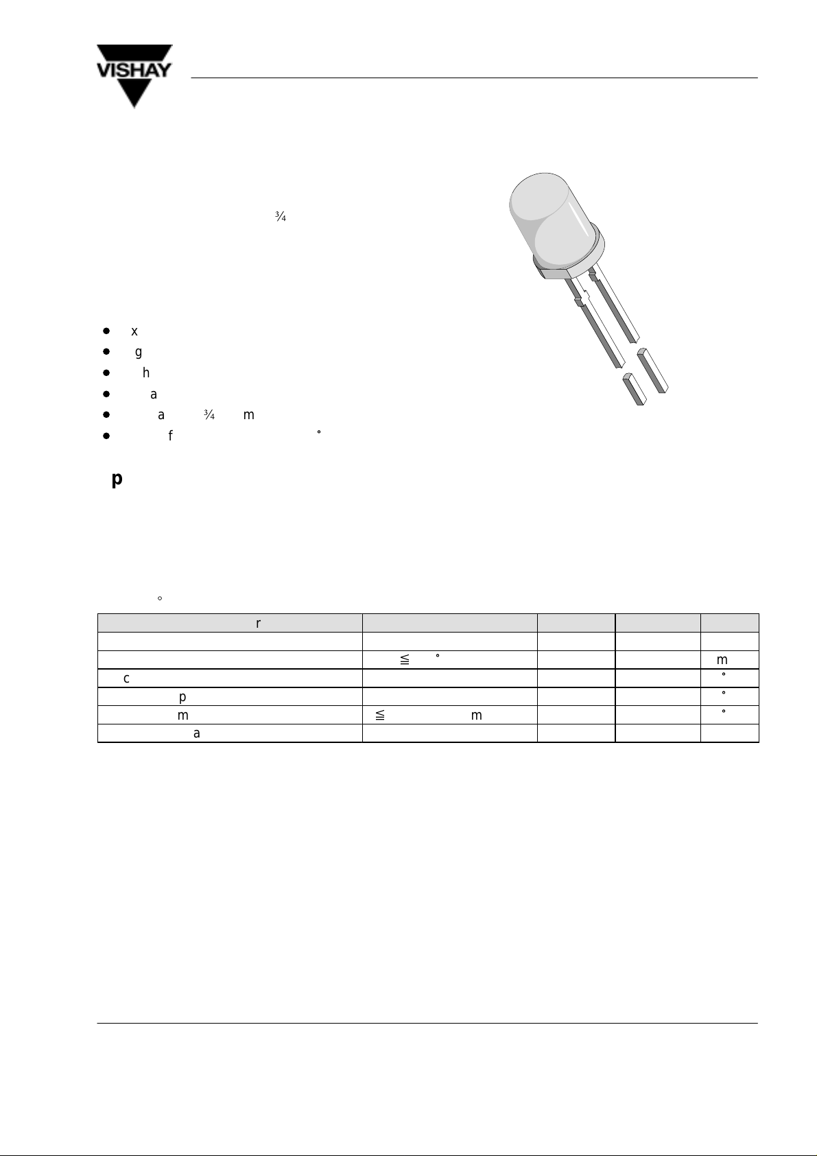
BPV10 is a very high speed and high sensitive PIN
photodiode in a standard T–1¾ plastic package.
Due to its waterclear epoxy the device is sensitive to
visible and infrared radiation.
94 8390
Features
D
Extra fast response times
D
High bandwidth B = 250 MHz at VR=12 V
D
High photo sensitivity
D
Radiant sensitive area A=0.78mm
D
Standard T–1¾ (ø 5 mm) package with clear lens
D
Angle of half sensitivity ϕ = ± 20
2
°
Applications
Wide band detector for demodulation of fast signals, industrial electronics, measurement, control circuits and
fast interrupters
Absolute Maximum Ratings
T
= 25_C
amb
Parameter Test Conditions Symbol Value Unit
Reverse Voltage V
Power Dissipation T
Junction Temperature T
Storage Temperature Range T
Soldering Temperature t x 5 s, 2 mm from body T
Thermal Resistance Junction/Ambient R
x 25 °C P
amb
R
V
j
stg
sd
thJA
60 V
215 mW
100
–55...+100
260
350 K/W
°
C
°
C
°
C
Document Number 81502
Rev. 3, 20-May-99
www.vishay.de • FaxBack +1-408-970-5600
1 (5)
Page 2
BPV10
g
g
Vishay Telefunken
Basic Characteristics
T
= 25_C
amb
Parameter Test Conditions Symbol Min Typ Max Unit
Forward Voltage IF = 50 mA V
Breakdown Voltage IR = 100 mA, E = 0 V
Reverse Dark Current VR = 20 V, E = 0 I
Diode Capacitance VR = 0 V, f = 1 MHz, E = 0 C
VR = 5 V, f = 1 MHz, E = 0 C
Open Circuit Voltage EA = 1 klx V
Ee = 1 mW/cm2, l = 950 nm V
Short Circuit Current EA = 1 klx I
Ee = 1 mW/cm2, l = 950 nm I
Reverse Light Current EA = 1 klx, VR = 5 V I
Ee = 1 mW/cm2,
l
= 950 nm, VR = 5 V
F
(BR)
ro
D
D
o
o
k
k
ra
I
ra
60 V
38 70
Absolute Spectral Sensitivity VR = 5 V, l = 950 nm s(l) 0.55 A/W
Angle of Half Sensitivity ϕ ±20 deg
Wavelength of Peak Sensitivity
Range of Spectral Bandwidth
Quantum Efficiency
l
= 950 nm
l
p
l
0.5
h
Noise Equivalent Power VR = 20 V, l = 950 nm NEP 3x10
Detectivity VR = 20 V, l = 950 nm D
Rise Time VR = 50 V, RL = 50 W,
l
= 820 nm
Fall Time VR = 50 V, RL = 50 W,
l
= 820 nm
*
t
r
t
f
1.0 1.3 V
1 5 nA
11 pF
3.8 pF
480 mV
450 mV
80
65
85
m
m
m
m
920 nm
570...1040 nm
72 %
3x10
–14
12
W/√ Hz
cm√Hz/
W
2.5 ns
2.5 ns
A
A
A
A
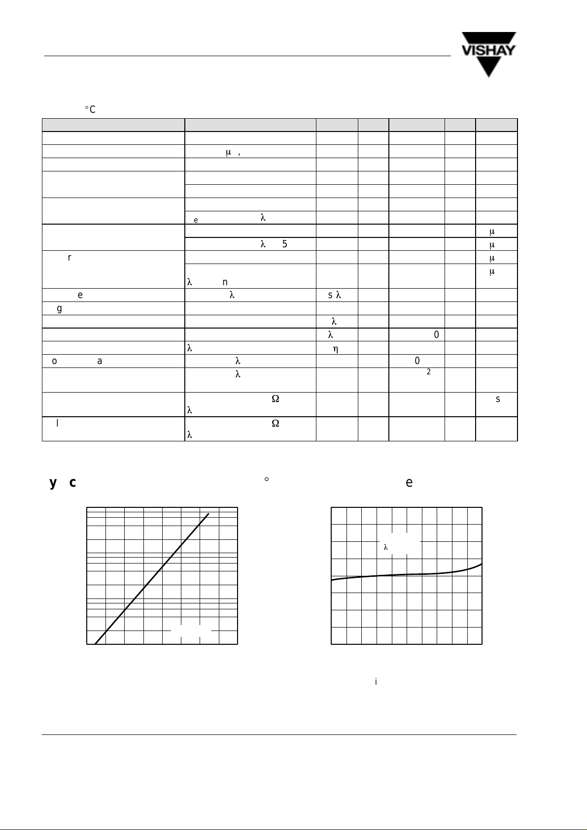
Typical Characteristics (T
1000
100
10
ro
I – Reverse Dark Current ( nA )
1
20 40 60 80
T
94 8436
Figure 1. Reverse Dark Current vs. Ambient Temperature
www.vishay.de • FaxBack +1-408-970-5600
2 (5) Rev. 3, 20-May-99
– Ambient Temperature ( °C )
amb
VR=20V
= 25_C unless otherwise specified)
amb
1.4
VR=5V
l
=950nm
– Ambient Temperature ( °C )
amb
Ambient Temperature
100
1.2
1.0
0.8
ra rel
I – Relative Reverse Light Current
0.6
020406080
94 8416
Figure 2. Relative Reverse Light Current vs.
T
100
Document Number 81502
Page 3

m
1000
100
BPV10
Vishay Telefunken
1.0
0.8
10
1
ra
I – Reverse Light Current ( A )
VR=5V
l
=950nm
0.1
0.01 0.1 1
94 8437
Ee – Irradiance ( mW/cm2 )
10
Figure 3. Reverse Light Current vs. Irradiance
m
ra
I – Reverse Light Current ( A )
94 8438
100
1mW/cm
10
0.05mW/cm
0.02mW/cm
1
0.1 1 10
0.5mW/cm
0.2mW/cm
0.1mW/cm
V
2
2
2
2
2
2
– Reverse Voltage ( V )
R
l
=950nm
100
Figure 4. Reverse Light Current vs. Reverse Voltage
0.6
0.4
rel
0.2
l
S ( ) – Relative Spectral Sensitivity
0
1150
94 8440
350 550 750 950
l
– Wavelength ( nm )
Figure 6. Relative Spectral Sensitivity vs. Wavelength
0°
10°20
°
30°
40°
1.0
0.9
0.8
rel
S – Relative Sensitivity
0.7
50°
60°
70°
80°
0.6
94 8624
0.4 0.2 0 0.2 0.4
0.6
Figure 7. Relative Radiant Sensitivity vs.
Angular Displacement
12
10
8
E=0
f=1MHz
6
4
D
C – Diode Capacitance ( pF )
2
0
0.1 1 10
94 8439
VR – Reverse Voltage ( V )
Figure 5. Diode Capacitance vs. Reverse Voltage
Document Number 81502
Rev. 3, 20-May-99
100
www.vishay.de • FaxBack +1-408-970-5600
3 (5)
Page 4

BPV10
Vishay Telefunken
Dimensions in mm
9612199
www.vishay.de • FaxBack +1-408-970-5600
4 (5) Rev. 3, 20-May-99
Document Number 81502
Page 5

BPV10
Vishay Telefunken
Ozone Depleting Substances Policy Statement
It is the policy of Vishay Semiconductor GmbH to
1. Meet all present and future national and international statutory requirements.
2. Regularly and continuously improve the performance of our products, processes, distribution and operating
systems with respect to their impact on the health and safety of our employees and the public, as well as their
impact on the environment.
It is particular concern to control or eliminate releases of those substances into the atmosphere which are known as
ozone depleting substances (ODSs).
The Montreal Protocol (1987) and its London Amendments (1990) intend to severely restrict the use of ODSs and
forbid their use within the next ten years. V arious national and international initiatives are pressing for an earlier ban
on these substances.
Vishay Semiconductor GmbH has been able to use its policy of continuous improvements to eliminate the use of
ODSs listed in the following documents.
1. Annex A, B and list of transitional substances of the Montreal Protocol and the London Amendments respectively
2. Class I and II ozone depleting substances in the Clean Air Act Amendments of 1990 by the Environmental
Protection Agency (EPA) in the USA
3. Council Decision 88/540/EEC and 91/690/EEC Annex A, B and C (transitional substances) respectively.
Vishay Semiconductor GmbH can certify that our semiconductors are not manufactured with ozone depleting
substances and do not contain such substances.
We reserve the right to make changes to improve technical design and may do so without further notice.
Parameters can vary in different applications. All operating parameters must be validated for each customer application
by the customer. Should the buyer use Vishay-Telefunken products for any unintended or unauthorized application, the
buyer shall indemnify Vishay-Telefunken against all claims, costs, damages, and expenses, arising out of, directly or
indirectly , any claim of personal damage, injury or death associated with such unintended or unauthorized use.
Document Number 81502
Rev. 3, 20-May-99
Vishay Semiconductor GmbH, P.O.B. 3535, D-74025 Heilbronn, Germany
Telephone: 49 (0)7131 67 2831, Fax number: 49 (0)7131 67 2423
www.vishay.de • FaxBack +1-408-970-5600
5 (5)
 Loading...