

Page 1

BRIGHT BM29F400T/BM29F400B
RESET
RESET
RESET
RESET
Microelectronics
Inc.
4MEGABIT (512K × 8/ 256K × 16)
5VOLT SECTOR ERASE CMOS FLASH MEMORY
GENERAL DESCRIPTION
The BM29F400 is an 4 Megabit, 5.0 volt-only CMOS Flash memory device organized as a 512
Kbytes of 8-bits each, or 256 Kbytes of 16 bits each. The device is offered in standard 48-pin TSOP
package. It is designed to be programmed and erased in-system with a 5.0 volt power-supply and can
also be reprogrammed in standard EPROM programmers.
With access times of 90 nS, 120 nS, and 150 nS, the BM29F400 has separate chip enable CE, write
enable WE, and output enable OE controls. BMI's memory devices reliably store memory data even
after 100,000 program and erase cycles.
The BM29F400 is entirely pin and command set compatible with the JEDEC standard for 4 Megabit
Flash memory devices. Commands are written to the command register using standard
microprocessor write timings. Register contents serve as input to an internal state-machine which
controls the erase and programming circuitry. Write cycles also internally latch addresses and data
needed for the programming and erase operations.
The BM29F400 is programmed by executing the program command sequence. This will start the
internal byte/word programming algorithm that automatically times the program pulse width and also
verifies the proper cell margin. Erase is accomplished by executing either the sector erase or chip
erase command sequence. This will start the internal erasing algorithm that automatically times the
erase pulse width and also verifies the proper cell margin. No preprogramming is required prior to
execution of the internal erase algorithm. Sectors of the BM29F400 Flash memory array are
electrically erased via Fowler-Nordheim tunneling. Bytes/words are programmed one byte/word at a
time using a hot electron injection mechanism.
The BM29F400 features a sector erase architecture. The device memory array is divided into one 16
Kbytes, two 8 Kbytes, one 32 Kbytes, and seven 64 Kbytes. Sectors can be erased individually or in
groups without affecting the data in other sectors. Multiple sector erase and full chip erase capabilities
add flexibility to altering the data in the device. To protect this data from accidental program and
erase, the device also has a sector protect function. This function hardware write protects the
selected sector(s). The sector protect and sector unprotect features can be enabled in a PROM
programmer.
For read, program and erase operation, the BM29F400 needs a single 5.0 volt power-supply.
Internally generated and well regulated voltages are provided for the program and erase operation. A
low Vcc detector inhibits write operations on loss of power. End of program or erase is detected by the
Ready/Busy status pin, Data Polling of DQ7, or by the Toggle Bit I feature on DQ6. Once the program
or erase cycle has been successfully completed, the device internally resets to the Read mode.
The BM29F400 also has a hardware
Internal Programming or Erase command will terminate the operation and reset the device to the
Read mode. The
access to boot code upon completion of system reset, even if the Flash device is in the process of an
Internal Programming or Erase operation. If the device is reset using the
Internal Programming or Erase operation, data in the address locations on which the internal state
A Winbond Company Publication Release Date: December 1999
- 1 - Revision A2
pin may be tied to the system reset circuitry, so that the system will have
pin. Driving the
pin low during execution of an
pin during an
Page 2
BRIGHT BM29F400T/BM29F400B
RESET
CE
OE
Microelectronics
Inc.
machine is operating will be erroneous. Thus, these address locations will need rewriting after the
device is reset.
FEATURES
•
5.0V +/- 10% Program and Erase
− Minimizes system-level power requirements
High performance
− 90 nS access time
•
Compatible with JEDEC-standard Commands
− Uses software commands, pinouts, and
packages following industry standards for
single power supply Flash memory
•
Typically 100,000 Program/Erase Cycles
•
Sector Erase Architecture
− One 16 Kbytes, two 8 Kbytes, one 32 Kbytes,
and seven 64 Kbytes
−
Any combination of sectors can be erased
concurrently; also supports full chip erase
•
Erase Suspend/Resume
− Suspend a sector erase operation to allow a
data read in a sector not being erased within
the same device
•
Ready/Busy
− RY/BY output pin for detection of
programming or erase cycle completion
•
− Hardware pin resets the internal state
machine to the read mode
•
Internal Erase Algorithms
− Automatically erases a sector, any
combination of sectors, or the entire
chip
•
Internal Programming Algorithms
− Automatically programs and verifies data at a
specified address
•
Low Power Consumption
− 20 mA typical active read current for Byte
Mode
− 28 mA typical active read current for Word
Mode
− 30 mA typical write/erase current
•
Sector Protection
− Hardware method disables any combination
of sectors from a program or erase operation
•
Boot Code Sector Architecture
FAMILY PART NO.
-90 -120 -150
Maximum Access Time (nS) 90 120 150
(E) Access time (nS)
(G) Access time (nS)
90 120 150
35 50 60
*This speed is available with Vcc = 5V +/- 5% variation
- 2 -
Page 3
BRIGHT BM29F400T/BM29F400B
CE
OE
WE
RESET
RESET
BYTE
Microelectronics
Inc.
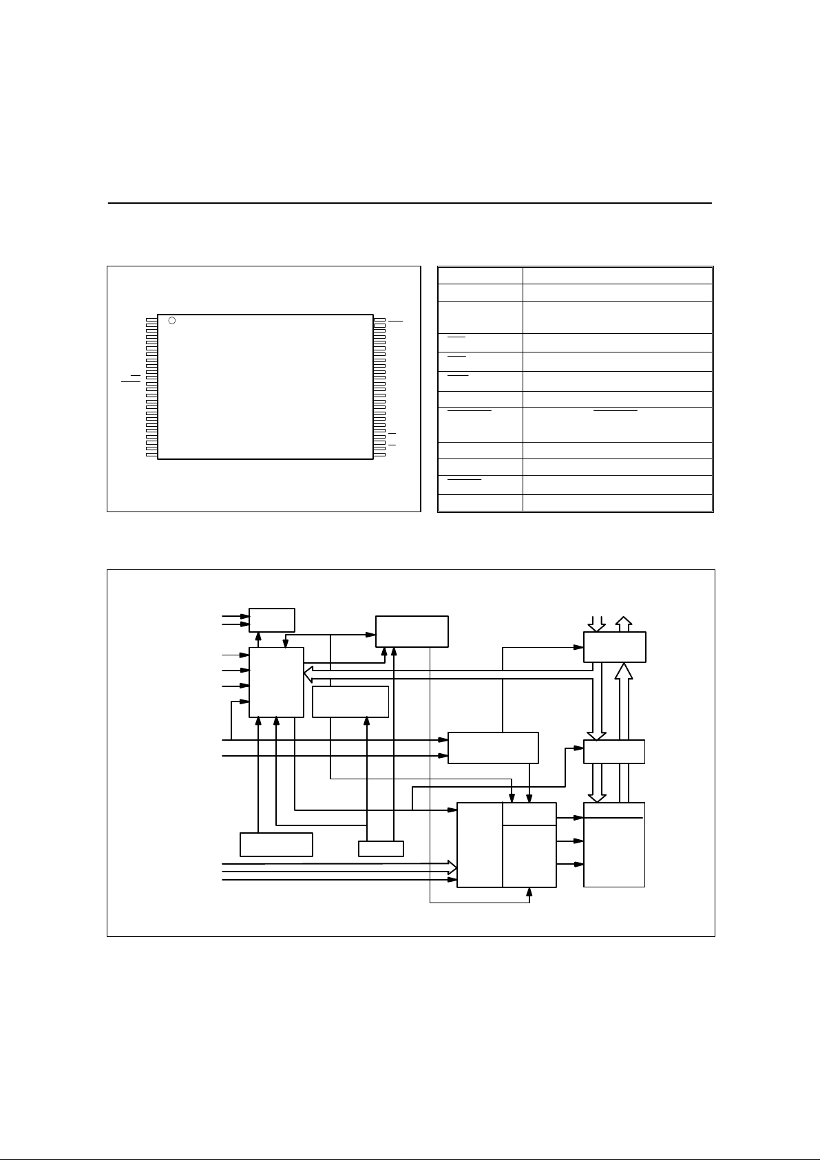
PIN CONFIGURATIONS
1
A15
2
A14
3
A13
4
A12
5
A11
6
A10
7
A9
8
A8
9
NC
10
NC
11
WE
12
RESET
13
NC
14
NC
15
RY/BY
16
NC
17
A17
18
A7
19
A6
20
A5
21
A4
22
A3
23
A2
24
A1
Standard TSOP
BLOCK DIAGRAM
Vcc
Vss
/WE
/BYTE
/RESET
RY/BY
Buffer
State
Control
Command
Register
48
47
46
45
44
43
42
41
40
39
38
37
36
35
34
33
32
31
30
29
28
27
26
25
PGM Voltage
Generator
A16
BYTE
Vss
DQ15/A-1
DQ7
DQ14
DQ6
DQ13
DQ5
DQ12
DQ4
Vcc
DQ11
DQ3
DQ10
DQ2
DQ9
DQ1
DQ8
DQ0
OE
Vss
CE
A0
Erase Boltage
Generator
PIN DESCRIPTION
A0−A17
DQ0−DQ14
DQ15/A-1 Data Input/Output, Address
VSS Device Ground
RY/BY Ready/Busy Status Output
VCC Device Power Supply
NC Not Internally Connected
Address Inputs
Data Input/Output
Max.
Chip Enable
Output Enable
Write Enable
Hardware
Active Low
Selects 8-bit or 16-bit Mode
DQ0-DQ15
Input/Output
Buffers
Pin,
/CE
/OE
Chip Enable
Output Enable
Logic
STB
Data Latch
STB
Y-Gating
Cell Matrix
A0-A16
Vcc Detector
Timer
Address
Latch
Y-Decodor
X-Decoder
A-1
A Winbond Company Publication Release Date: December 1999
- 3 - Revision A2
Page 4
BRIGHT BM29F400T/BM29F400B
BYTE
BYTE
Microelectronics
Inc.
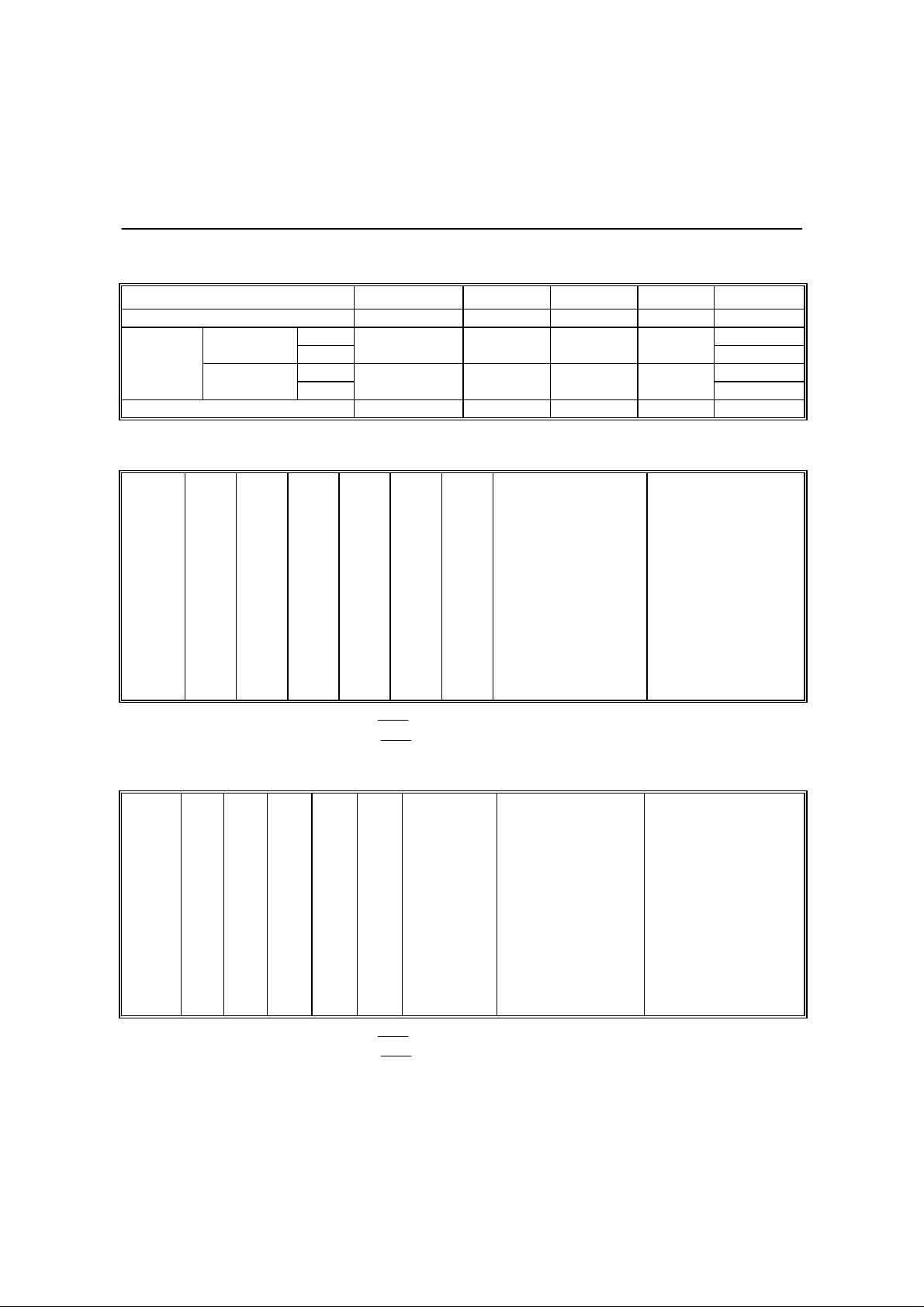
BUS OPERATION
OE
OE
(1)
A0 A1 A6 A9 DQ0-DQ15
WE
(1)
A0 A1 A6 A9 DQ0-DQ7 DQ8-DQ15
WE
(4)
IN
High Z H
OUT
H
(4)
H
RESET
Table 1. Bus Operations
OPERATION
Electronic ID Manufacturer
Electronic ID Device
(3)
Read
L L H A0 A1 A6 A9 D
Standby H X X X X X X High Z H
Hardware Reset X X X X X X X High Z L
Output Disable L H H X X X X High Z X
Write L H L A0 A1 A6 A9 DIN
Verify Sector Protect
Temporary Sector Unprotect X X X X X X X X VID
Notes:
1. L = VIL, H = VIH, X = Don't Care. See DC Characteristics for voltage levels.
2. Manufacturer and device codes may also be accessed via a command register sequence. Refer to Table 6.
3. WE can be V
4. Refer to Table 6 for valid DIN during a write operation.
IL
if CE is VIL, OE at VIH initiates the write operations.
(2)
(2)
L L H H L L VID Code H
(2)
L L H L H L VID Code H
Table 2. Bus Operations
OPERATION
Electronic ID Manufacturer
Electronic ID Device
(3)
Read
L L H A0 A1 A6 A9 DOUT High Z H
Standby H X X X X X X High Z High Z H
Hardware Reset X X X X X X X High Z High Z L
Output Disable L H H X X X X High Z High Z H
Write L H L A0 A1 A6 A9 D
Verify Sector Protect
Temporary Sector Unprotect X X X X X X X X High Z VID
Notes:
1. L = VIL, H = VIH, X = Don't Care. See DC Characteristics for voltage levels.
2. Manufacturer and device codes may also be accessed via a command register sequence. Refer to Table 6.
3. WEcan be VIL if CE is VIL, OE at VIH initiates the write operations.
4. Refer to Table 6 for valid DIN during a write operation.
(2)
(2)
L L H H L L VID Code High Z H
(2)
L L H L H L VID Code High Z H
(
L L H L L L VID Code H
(
L L H L L L VID Code High Z H
CE
= VIH)
CE
= VIL)
RESET
- 4 -
Page 5
BRIGHT BM29F400T/BM29F400B
Microelectronics
Inc.
Table 3. Sector Protection Verify Electronic ID Codes
TYPE A17-A12 A6 A1 A0 Code (Hex)
Manufacturer Code
29F400T Byte X VIL VIL VIH 23H
29F400 Word 22,23H
29F400B Byte X VIL VIL VIH ABH
Word 22 ABH
Sector Protection Sector Address VIL VIH VIL 01H(1)
Note: Outputs 01H at protected sector addresses, and outputs 00H at unprotected addresses.
Table 4. Sector Address Tables (BM29F400T)
A17 A16 A15 A14 A13 A12 (x8) Address Range (x16) Address Range
SA0 0 0 0 X X X 00000H-0FFFFH 00000H-07FFFH
SA1 0 0 1 X X X 10000H-1FFFFH 08000H-0FFFFH
SA2 0 1 0 X X X 20000H-2FFFFH 10000H-17FFFH
SA3 0 1 1 X X X 30000H-3FFFFH 18000H-1FFFFH
SA4 1 0 0 X X X 40000H-4FFFFH 20000H-27FFFH
SA5 1 0 1 X X X 50000H-5FFFFH 28000H-2FFFFH
SA6 1 1 0 X X X 60000H-6FFFFH 30000H-37FFFH
SA7 1 1 1 0 X X 70000H-77FFFH 38000H-3BFFFH
SA8 1 1 1 1 0 0 78000H -79FFFH 3C000H-3CFFFH
SA9 1 1 1 1 0 1 7A000H -7BFFFH 3D000H-3DFFFH
SA10 1 1 1 1 1 X 7C000H-7FFFFH 3E000H-3FFFFH
Notes:
1. The address range is A17:A-1 if in byte mode (
2. The address range is A17:A0, if in word mode (
X VIL VIL VIL ADH
= VIL).
BYTE
= VIH).
BYTE
Table 5. Sector Address Tables (BM29F400B)
A17 A16 A15 A14 A13
SA0 0 0 0 0 0 X 00000H-03FFFH 00000H-01FFFH
SA1 0 0 0 0 1 0 04000H-05FFFH 02000H-02FFFH
SA2 0 0 0 0 1 1 06000H-07FFFH 03000H-03FFFH
SA3 0 0 0 1 X X 08000H-0FFFFH 04000H-07FFFH
SA4 0 0 1 X X X 10000H-1FFFFH 08000H-0FFFFH
SA5 0 1 0 X X X 20000H-2FFFFH 10000H-17FFFH
SA6 0 1 1 X X X 30000H-3FFFFH 18000H-1FFFFH
SA7 1 0 0 X X X 40000H-4FFFFH 20000H-27FFFH
SA8 1 0 1 X X X 50000H-5FFFFH 28000H-2FFFFH
SA9 1 1 0 X X X 60000H-6FFFFH 30000H-37FFFH
SA10 1 1 1 X X X 70000H-7FFFFH 38000H-3FFFFH
Notes:
1. The address range is A17:A-1 if in byte mode (
2. The address range is A17:A0, if in word mode (
A Winbond Company Publication Release Date: December 1999
- 5 - Revision A2
BYTE
BYTE
A12
= VIL).
= VIH).
(x8) Address Range
x16) Address Range
Page 6

BRIGHT BM29F400T/BM29F400B
RESET
RESET
RESET
RESET
RESET
RESET
RESET
RESET
RESET
Microelectronics
Inc.
Electronic ID Mode
The Electronic ID mode allows the reading out of a binary code from the device and will identify its
manufacturer and device type. This mode is intended for use by programming equipment for the
purpose of automatically matching the device to be programmed with its corresponding programming
algorithm. This mode is functional over the entire temperature range of the device.
To activate this mode, the programming equipment must force VID (11.5V to 12.5V) on address pin
A9. Two identifier bytes may then be sequenced from the device outputs by toggling address A0 from
VIL to VIH. All addresses are don't cares except A0, A1, and A6 (see Table 3).
Manufacturer and device codes may also be read via the command register; for instance, when the
BM29F400 is erased or programmed in a system without access to high voltage on the A9 pin. The
command sequence is illustrated in Table 6 (refer to Electronic ID Command section).
Byte 0 (A0 = VIL) represents the manufacturer's code (Bright Microelectronics = ADH) and byte 1 (A0
= VIH) the device identifier code (BM29F400T = 23H and BM29F400B = ABH for 8-bit mode;
BM29F400T = 2223H and BM29F400B = 22ABH for 16-bit mode). These two byte words are given in
Table 3. To read the proper device codes when executing the Electronic ID, all identifiers for
manufacturer and device will exhibit odd parity with the MSB (DQ7) defined as the parity bit. A1 must
be VIL (see Table 3).
Read Mode
The BM29F400 has three control functions which must be satisfied in order to obtain data at the
outputs. CE is the power control and should be used for device selection. OE is the output control
and should be used to gate data to the output pins if a device is selected. As shown in Table 1, WE
should be held at VIH, except in Write mode and Enable Sector Protect mode.
Address access time (t
enable access time (tCE) is the delay from stable addresses and stable CE to valid data at the output
pins. Output enable access time is the delay from the falling edge of OE to valid data at the output
pins (assuming the addresses have been stable for at least t
Standby Mode and Hardware
The BM29F400 has two methods for implementing standby mode. The first method requires use of
both the CE pin and the
When using both pins, a CMOS standby mode is achieved when both CE and
Vcc ±0.5V. In this condition, the current consumed is typically less than 100 µA. A TTL standby mode
is achieved with both CE and
reduced to 200 µA. The device can be read with standard access time (tCE) from either of these two
standby modes.
When using the
±
0.5V. In this condition, the current consumed is typically less than 100 µA. A TTL standby mode is
achieved with
Once the
valid for a read access.
pin is taken high, the device requires 500 nS of wake-up time before outputs are
) is equal to the delay from stable addresses to valid output data. Chip
ACC
−
tOE time).
ACC
Standby Mode
pin. The second method only requires use of the
held at VIH. In this condition, the typical current required is
pin only, a CMOS standby mode is achieved with
held at VIL. In this condition, the typical current required is reduced to 1 mA.
pin.
are held at
held at VSS
- 6 -
Page 7

BRIGHT BM29F400T/BM29F400B
RESET
RESET
Microelectronics
Inc.
If the device is deselected during programming or erase, the device will draw active current until the
programming or erase operation is completed. In the standby mode the outputs are in a high
impedance state, independent of the OE input.
Output Disable Mode
With the OE input at a logic high level (VIH), output from the device is disabled. This will cause the
output pins to be in a high impedance state. It is shown in Table 1 that CE = VIL and WE = VIH for
Output Disable. This is to differentiate Output Disable mode from Write mode and to prevent
inadvertent writes during Output Disable.
Program and Erase Modes
Device programming and erase are accomplished via the command register. Contents of the register
serve as inputs to the internal state machine. Outputs of the state machine dictate the function of the
device.
The command register itself does not occupy any addressable memory locations. The register is a
latch used to store the commands along with the addresses and data information needed to execute
the command. The command register is written by bringing WE to VIL, while CE is at VIL and OE is
at VIH. Addresses are latched on the falling edge of WE or CE, whichever happens later, while data
is latched on the rising edge of WE or CE, whichever happens first. Standard microprocessor write
timings are used. Refer to AC Characteristics for Programming/Erase and their respective Timing
Waveforms for specific timing parameters.
Enable Sector Protect and Verify Sector Protect Modes
The BM29F400 has a hardware Sector Protect mode that disables both Programming and Erase
operation to the protected sector(s). There are total of 11 sectors in this device. The sector protect
feature is enabled using the programming equipment at the user's site. The device is shipped from
the BMI factory with all sectors unprotected.
To verify programming of the protection circuitry, the programming equipment must force VID on the
address pin A9 with CE and OE at VIL and WE at VIH. As shown in Table 2, scanning the sector
addresses while (A6, A1 and A0) = (0, 1, 0) will produce a 01H code at the device output pins for a
protected sector. In the Verify Sector Protect mode, the device will read 00H for an unprotected
sector. In this mode, the lower order addresses, except for A0, A1 and A6, are don't care. Address
locations with A1 = VIL are reserved for Electronic ID manufacturer and device codes. It is also
possible to determine if a sector is protected in-system by writing the Electronic ID command
(described in the Electronic ID command section below.)
Temporary Sector Unprotect Mode
The BM29F400 has a Temporary Sector Unprotect feature that allows the protect feature to be
temporarily suspended to change data in a protected sector in-system. The Temporary Sector
Unprotect mode is activated by setting the
In this mode, protected sectors can be programmed or erased by selecting the sector addresses.
Once VID is removed from the
the Temporary Sector Unprotect algorithm and timing waveforms.
A Winbond Company Publication Release Date: December 1999
- 7 - Revision A2
pin, all previously protected sectors will be protected. Refer to
pin to VID (11.5V−12.5V).
Page 8

BRIGHT BM29F400T/BM29F400B
RESET
RESET
RESET
Microelectronics
Inc.
Read
The read or
command register. Microprocessor read cycles retrieve the data from the memory. The device
remains enable for reads until the command register contents are changed.
The device will automatically power-up in the Read/Reset mode. In this case, a command sequence
is not needed to read the memory data. This default power-up to Read mode ensures that no spurious
changes of the data can take place during the power transitions. Refer to the AC Characteristics for
Read-Only Operation and the respective Timing Waveforms for the specific timing parameters.
Electronic ID Command
The BM29F400 contains an Electronic ID command to supplement the traditional PROM
programming method described in the Electronic ID Mode section. The operation is initiated by writing
the Electronic ID command sequence into the command register. Following command write, a read
cycle from address XX00H retrieves manufacturer code of ADH. A read cycle from address XX01H
returns the device code (BM29F400T = 23H and BM29F400B = ABH for 8-bit mode; BM29F400T =
2223H and BM29F400B = 22ABH for 16-bit mode) (see Table 3). All manufacturer and device codes
exhibit odd parity with the MSB (DQ7) defined as the parity bit.
The Electronic ID command can also be used to identify protected sectors. After writing the Electronic
ID command sequence, the CPU can scan the sector addresses (see Table 4 and Table 5) while (A6,
A1, A0) = (0, 1, 0). Protected sectors will return 01H on the data outputs and unprotected sectors will
return 00H. To terminate the operation, it is necessary to write the Read/Reset command sequence
into the command register.
Byte/Word Programming Command
Command
operation is initiated by writing the Read/Reset command sequence in to the
The device is programmed on a byte-by-byte (or word-by-word) basis. Programming is a four bus
cycle operation (see Table 6). There are two "unlock" write cycles. These are followed by the program
set-up command and data write cycles. Addresses are latched on the falling edge of CE or WE,
whichever happens later, and program data (PD) is latched on the rising edge of CE or WE,
whichever happens first. The rising edge of CE or WE, whichever happens first, begins
programming using the Embedded Program Algorithm.
Upon executing the algorithm, the system is not required to provide further controls or timings. The
device will automatically provide adequate internally generated program pulses and verify the
programmed cell margin.
The automatic programming operation is completed when the data on DQ7 (also used as Data
Polling) is equivalent to the data written to this bit at which time the device returns to the read mode
and addresses are no longer latched (see Table 7, Write Operation Status Flags). Therefore, the
device requires that a valid address to the device be supplied by the system at this particular instance
of time for
being programmed.
Any commands written to the chip during the Internal Program Algorithm will be ignored. If a
hardware
be corrupted.
Data
Polling operations.
Data
Polling must be performed at the memory location which is
occurs during the programming operation, the data at that particular location will
- 8 -
Page 9

BRIGHT BM29F400T/BM29F400B
RESET
RESET
Microelectronics
Inc.
Byte/Word programming is allowed in any sequence, and across sector boundaries. However,
remember that a data "0" cannot be programmed to a data "1". Only erase operations can convert a
logical "0" to a logical "1". Attempting to program data from "0" to "1" may cause the device to exceed
time limits, or even worse, result in an apparent success according to the Data Polling algorithm. In
the later case, however, a subsequent read of this bit will show that the data is still a logical "0".
Figure 1 illustrates the Byte/Word Programming Algorithm using typical command strings and bus
operations.
The device will ignore any commands written to the chip during execution of the internal Byte/Word
Programming Algorithm. If a hardware
the data at that particular address location will be corrupted.
Chip Erase Command
Chip erase is a six bus cycle operation (see Table 6). The chip erase begins on the rising edge of the
last WE pulse in the command sequence.
Upon executing the Chip Erase command sequence, the device's internal state machine executes an
internal erase algorithm. The system is not required to provide further controls or timings. The device
will automatically provide adequate internally generated erase pulses and verify chip erase within the
proper cell margins. During chip erase, all sectors of the device are erased except protected sectors.
occurs during the Byte/Word Programming operation,
During Chip Erase, data bit DQ7 shows a logical "0". This operation is known as
erase operation is completed when the data on DQ7 is a logical "1" (see Write Operation Status
section). Upon completion of the Chip Erase operation, the device returns to read mode. At this time,
the address pins are no longer latched. Note that Data Polling must be performed at a sector address
within any of the sectors being erased and not a protected sector to ensure that DQ7 returns a logical
"1" upon completion of the Chip Erase operation.
Figure 2 illustrates the Chip Erase Algorithm using typical command strings and bus operations.
The device will ignore any commands written to the chip during execution of the internal Chip Erase
algorithm. If a hardware
be corrupted.
Sector Erase Command
Sector erase is a six bus cycle operation (see Table 6). The sector address (any address location
within the desired sector) is latched on the falling edge of WE, while the command data is latched on
the rising edge of WE. An internal device timer will initiate the Sector Erase operation 100 µS ±20%
(80 µS to 120 µS) from the rising edge of the WE pulse for the last Sector Erase command entered
on the device.
Upon executing the Sector Erase command sequence, the device's internal state machine executes
an internal erase algorithm. The system is not required to provide further controls or timings. The
device automatically provides adequate internally generated erase pulses and verify sector erase
within the proper cell margins. Protected sectors of the device will not be erased, even if they are
selected with the Sector Erase command.
occurs during the Chip Erase operation, the data in the device will
Data
Polling. The
A Winbond Company Publication Release Date: December 1999
- 9 - Revision A2
Page 10

BRIGHT BM29F400T/BM29F400B
RESET
RESET
RESET
RESET
RESET
Microelectronics
Inc.
Multiple sectors can be erased simultaneously by writing the sixth bus cycle command of the Sector
Erase command for each sector to be erased. The time between initiation of the next Sector Erase
command must be less than 80 µS to guarantee acceptance of the command by the internal state
machine. The time-out window can be monitored via the write operation status pin DQ3 (refer to the
Write Operation Status section for Sector Erase Timer operation). It is recommended that CPU
interrupts be disabled during this time to ensure that the subsequent Sector Erase commands can be
initiated within the 100 µS window. The interrupts can be re-enabled after the last Sector Erase
command is written. As mentioned above, an internal device timer will initiate the Sector Erase
operation 100 µS ±20% (80 µS to 120 µS) from the rising edge of the last WE pulse. Sector Erase
Timer Write Operation Status pin (DQ3) can be used to monitor time out window. If another falling
edge of the WE occurs within the 100 mS time-out window, the internal device timer is reset.
Loading the sector erase buffer may be done in any sequence and with any number of sectors.
Any command other than Sector Erase or Erase Suspend during this period and afterwards will
the device to read mode, ignoring the previous command string. Resetting the device with a
hardware
the operated sectors being undefined and may be unrecoverable. In this case, restart the Sector
Erase operation on those sectors and attempt to allow them to complete the Erase operation.
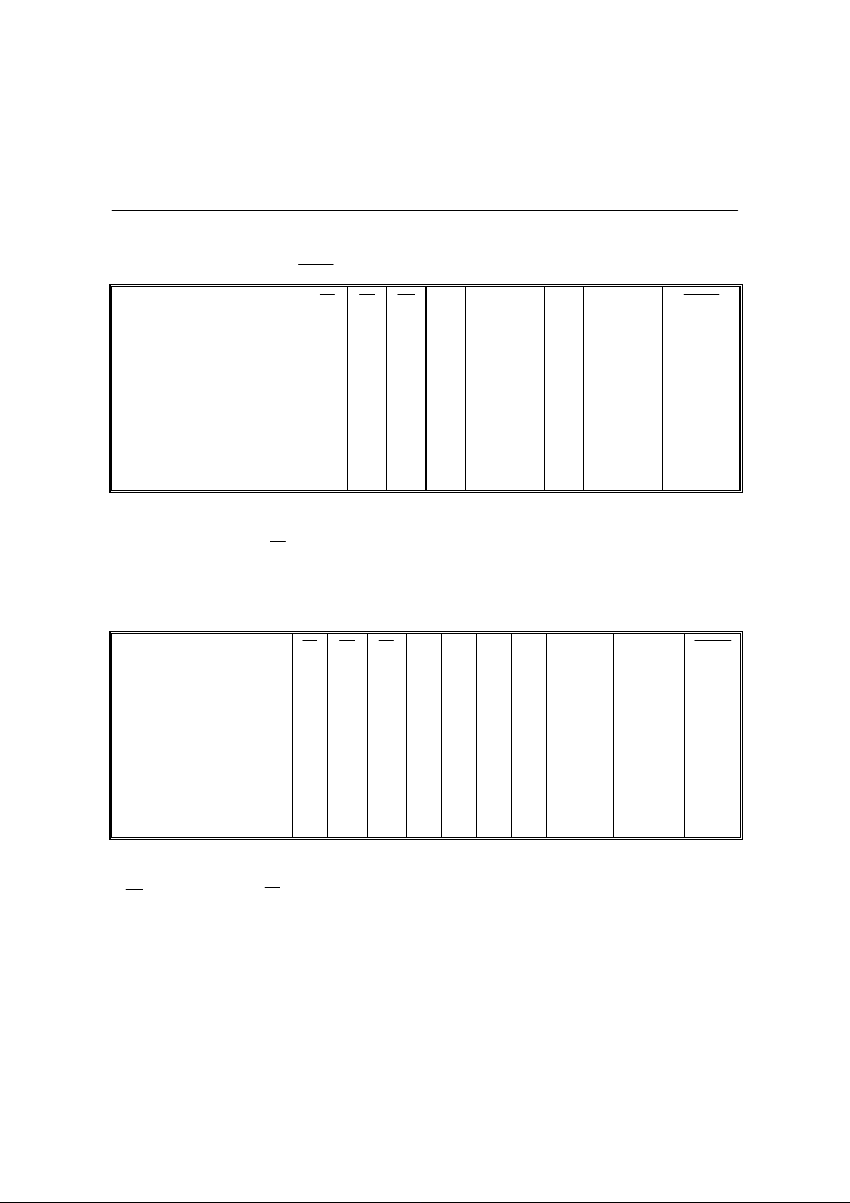
Command Definitions
after it has begun execution of a Sector Erase operation will result in the data in
Device operations are selected by writing specific address and data sequences in to the Command
register. Writing incorrect addresses and data values or writing them in the improper sequence will
the device to Read mode. Table 5 defines the valid register command sequences. Either of
the two Read/Reset commands will
During Sector Erase operation, data bit DQ7 shows a logical "0". This operation is known as
Polling. Sector Erase operation is complete when data on DQ7 is a logical "1" (see Write Operation
Status section) at which time the device returns to read mode. At this time, the address pins are no
longer latched. Note that Data Polling must be performed at a sector address within any of the
sectors being erased and not a protected sector to ensure that DQ7 returns a logical "1" upon
completion of the Sector Erase operation.
Figure 2 illustrates the Sector Erase Algorithm using typical command strings and bus operations.
During execution of the Sector Erase command, only the Erase Suspend and Erase Resume
commands are allowed. All other commands will
Note: Do not attempt to write an invalid command sequence during the sector erase operation. Doing so will terminate the sector
erase operation and the device will /RESET to the read mode.
the device (when applicable).
Data
the device to read mode.
- 10 -
Page 11
BRIGHT BM29F400T/BM29F400B
Electronic
(B Device ID)
(B Device ID)
Microelectronics
Inc.
Table 6. Command Definitions
Command
Sequence
Reset/Read Required Addr. Data Addr. Data Addr. Data Addr. Data Addr. Data Addr. Data
Reset/Read 1 XXXXH F0H
Reset Word 4 5555H AAH 2AAAH 55H 5555H F0H RA RD
/Read Byte AAAAH 5555H AAAAH
ID Byte AAAAH 5555H AAAAH 23H
Program Word 4 5555H AAH 2AAAH 55H 5555H A0H PA PD
Byte AAAAH 5555H AAAAH
Chip Word 6 5555H AAH 2AAAH 55H 5555H 80H 5555H AAH 2AAAH 55H 5555H 10H
Erase Byte AAAAH 5555H AAAAH AAAAH 5555H AAAAH
Sector Word 6 5555H AAH 2AAAH 55H 5555H 80H 5555H AAH 2AAAH 55H SA 30H
Erase Byte AAAAH 5555H AAAAH AAAAH 5555H
Erase Word 1 XXXXH B0H
Suspend Byte
Erase Word 1 XXXXH 30H
Resume Byte
Notes:
Bus Write
Cycles
Word 4 5555H AAH 2AAAH 55H 5555H 90H 01H
First Bus Write
Cycle
Second Bus
Write Cycle
Third Bus
Write Cycle
Fourth Bus Write
Cycle
(7)
2223H
(T Device ID)
22ABH
(T Device ID)
ABH
Fifth Bus Write
Cycle
Sixth Bus Write
Cycle
1. Bus operations are defined in Tables 1 and 2.
2. For a Command Sequence, address bit A15 = X = Don't Care for all address commands except for Program Address (PA) and
Sector Address (SA).
3. RA = Address of the memory location to be read.
RD = Data read from location RA during read operation.
PA = Address of the memory location to be programmed. Addresses are latched on the falling edge of the WE pulse.
PD = Data to be programmed at location PA. Data is latched on the rising edge of WE.
SA = Address of sector to be erased. (See Table 4 for top boot and Table 5 for bottom boot.)
4. The Erase Suspend (B0H) and Erase Resume (30H) commands are valid only while the Sector Erase operation is in
progress.
5. Reading from, and programming to, non-erasing sectors is allowed in the Erase Suspend mode.
6. The System should generate the following address patterns:
Word Mode: 5555H or 2AAAH to addresses A0−A14.
Byte Mode: AAAAH or 5555H to addresses A-1−A14.
7. Address 00H returns the manufacturer's ID code (Bright Microelectronics - ADH), address 01H returns the device ID code.
Erase Suspend/Erase Resume Commands
The Erase Suspend command allows the user to interrupt a Sector Erase operation and read data
from or to a sector that is not being erased. The Erase Suspend command is applicable only during
Sector Erase operation, including, but not limited to, sector erase time-out period after any Sector
Erase commands (30H) have been initiated.
A Winbond Company Publication Release Date: December 1999
- 11 - Revision A2
Page 12

BRIGHT BM29F400T/BM29F400B
RESET
Microelectronics
Inc.
Writing the Erase Suspend command during the time-out will result in immediate termination of the
time-out period. Any subsequent writes of the Sector Erase command will be taken as the Erase
Resume command (30H). Note that any other commands during the time-out will
to the Read mode. The address pins are "don't cares" when writing the Erase Suspend or Erase
Resume commands.
When the Erase Suspend command is written during a Sector Erase operation, the chip will take
between 1 µS and 230 µS to suspend the erase operation and go into Erase Suspended mode.
During this time, the system can monitor the Data Polling or Toggle Bit write operation status flags to
determine when the device has entered erase suspend mode (see Write Operation Status section.)
The system must use an address of an erasing sector to monitor Data Polling or Toggle Bit to
determine if the Sector Erase operation has been suspended.
In Erase Suspend mode, the system can read data from any sector that is not being erased. A read
from a sector being erased will result in write operation status data. After the system writes the Erase
Suspend command and waits until the Toggle Bit stops toggling, data reads from the device may then
be performed (see Write Operation Status section). Any further writes of the Erase Suspend
command at this time will be ignored.
To resume operation of Sector Erase, the Erase Resume command (30H) should be written. Any
further writes of the Erase Resume command at this point will be ignored. Another Erase Suspend
command can be written after the chip has resumed Sector Erase operation.
DQ7
the device
Polling
Data
The BM29F400 device features
Byte/Word Programming, Chip Erase, and Sector Erase operations. When the Byte/Word
Programming operation is in progress, an attempt to read the device will produce the compliment of
the data last written to DQ7. Upon completion of the Byte/Word Programming operation, an attempt
to read the device will produce the true data last written to DQ7. When the Chip Erase or Sector
Erase operation is in progress, an attempt to read the device will produce a logical "0" at the DQ7
output. Upon completion of the Chip Erase or Sector Erase operation, an attempt to read the device
will produce a logical "1" at the DQ7 output. The flowchart for Data Polling (DQ7) is shown in Figure
3.
For Chip Erase, the
pulse sequence. For Sector Erase, the Data Polling is valid after the last rising edge of the sector
erase WE pulse. For both Chip Erase and Sector Erase, Data Polling must be performed at sector
address within any of the sectors being erased and not a protected sector. Otherwise, the
Polling status may not be valid. Once the Internal Algorithm operation is close to being completed,
the BM29F400 data pins (DQ7) may change asynchronously while the output enable (OE) is
asserted low. This means that the device is driving status information on DQ7 at one instant and valid
data at the next instant of time. Depending on when the system samples the DQ7 output, it may read
status or valid data. Even if the device has completed the Internal Algorithm operation and DQ7 has a
valid data, data outputs on DQ0-DQ6 may be still invalid. Valid data on DQ0-DQ7 will be read on the
successive read attempts.
Data
Polling is valid after the rising edge of the sixth WE pulse in the six write
Data
Polling as a method to indicate to the host the status of the
Data
- 12 -
Page 13

BRIGHT BM29F400T/BM29F400B
BYTE
RESET
BYTE
Microelectronics
Inc.
Data
The
operation, Sector Erase Operation, or Sector Erase time-out window (see Table 7).
DQ6
Toggle Bit
The BM29F400 also features the "Toggle Bit" as a method to indicate to the host system the status of
the Internal Programming and Erase Algorithms (see Figure 4 for Toggle Bit (DQ6) flowchart.
During an Internal Programming or Erase Algorithm cycle, successive attempts to read (OE toggling)
data from the device will result in DQ6 toggling between one and zero. Once Internal Programming or
Erase operation is completed, DQ6 will stop toggling and valid data will be read on the next
successive attempts. During
fourth WE pulse in the four write pulse sequence. For Chip Erase, Toggle Bit is valid after the rising
edge of the sixth WEpulse in the six write pulse sequence. For Sector Erase, Toggle Bit is valid after
the last rising edge of the sector erase WE pulse. Toggle Bit is also active during sector erase time-
out window.
In Byte/Word Programming, if the sector being written to is protected, the Toggle Bit will toggle for
about 300 nS and then stop toggling without the data having changed. In Chip Erase or Sector Erase,
the device will erase all the selected sectors except for the ones that are protected. If all selected
sectors are protected, the chip will toggle the Toggle Bit for about 300 nS and then drop back into
read mode, having changed none of the data. Either CE or OE toggling will cause the DQ6 Toggle
Bit I to toggle.
DQ5
Exceeded Timing Limits
Polling feature is only active during the Byte/Word Programming operation, Chip Erase
Programming, Toggle Bit is valid after the rising edge of the
DQ5 will indicate if the Byte/Word Programming, Chip Erase, or Sector Erase time has exceeded the
specified limits (internal pulse count) of the device. Under these conditions DQ5 will produce a logical
"1". This is a failure condition which indicates that the program or erase cycle was not successfully
completed.
and WE pins will control the output disable functions as described in Table 1.
If this failure condition occurs during Sector Erase operation, it specifies that particular sector is bad
and it may not be reused. However, other sectors are still functional and may continue to be used for
the program or erase operation. The device must be
of the device. Write the Read/Reset command sequence to the device, and then execute the
Byte/Word Programming or Sector Erase command sequence. This allows the system to continue to
use the other active sectors in the device.
If this failure condition occurs during Chip Erase operation, it specifies that the entire chip is bad or
combination of sectors are bad. In so, the chip should not be reused.
If this failure condition occurs during Byte/Word Programming operation, it indicates the entire sector
containing that
can be reused.)
A Winbond Company Publication Release Date: December 1999
- 13 - Revision A2
Data
Polling is the only operating function of the device under this condition. The OE
to the Read mode to use other sectors
is bad and this sector may not be reused (other sectors are still functional and
Page 14

BRIGHT BM29F400T/BM29F400B
Microelectronics
Inc.
The DQ5 failure condition may also appear if a user tries to program a non blank location without
erasing. In this case, the device may exceed time limits and not complete the Internal Algorithm
operation. Hence, the system never reads a valid data on DQ7 bit and DQ6 never stops toggling.
Once the device has exceeded timing limits, the DQ5 bit will indicate a "1".
DQ3
Sector Erase Timer
After the completion of the initial Sector Erase command sequence, the sector erase time-out window
will begin. DQ3 will remain low until the time-out window is closed. Data Polling and Toggle Bit are
valid after the initial Sector Erase command sequence.
Data
If
DQ3 maybe used to determine if the Sector Erase time-out window is still open. If DQ3 is a logical
"1", the internally controlled erase cycle has begun. Attempts to write subsequent command to the
device will be ignored until the erase operation is completed as indicated by Data Polling or Toggle
Bit. If DQ3 is a logical "0", the device will accept additional Sector Erase commands. To ensure the
command has been accepted, the system software should check the status of DQ3 prior to and
following each subsequent Sector Erase command. If DQ3 were high on the second status check, the
command may not have been accepted. Refer to Table 7: Write Operation Status Flags.
Polling or the Toggle Bit indicates the device has been written with a valid erase command,
Write Operations Status
STATUS DQ7 DQ6 DQ5 DQ3
In Byte/Word Programming Operation
Progress Chip or Sector Erase Operation 0 Toggle 0 1
Exceeded Byte/Word Programming Operation
Time Limits Chip or Sector Erase Operation 0 Toggle 1 1
Notes: DQ0, DQ1, DQ4 are reserve pins for future use.
Erase Suspend Mode
(Non-Erase Suspended Sector)
Table 7. Write Operation Status Flags
DQ7
Data Data Data Data
DQ7
Toggle 0 N/A
Toggle 1 0
(1)
RY/BY
Ready/Busy Status
The BM29F400 provides a RY/BY open-drain output pin as a way to indicate to the host system that
an Internal Programming or Erase operation is either in progress or has been completed. If the RY/BY
output is low, the device is busy with either a Programming or Erase operation. If the RY/BY output is
high, the device is ready to accept a Read, Programming, or Erase command. When the RY/BY pin
is low, the device will not accept any additional Programming or Erase commands with the exception
of the Erase Suspend command. If the BM29F400 is placed in an Erase Suspend mode, the RY/BY
output will be high.
- 14 -
Page 15

BRIGHT BM29F400T/BM29F400B
RESET
RESET
RESET
RESET
RESET
RESET
RESET
RESET
RESET
RESET
RESET
RESET
RESET
RESET
RESET
RESET
RESET
RESET
Microelectronics
Inc.
During a programming operation, the RY/BY pin is driven low after the rising edge of the fourth WE
pulse. During an erase operation, the RY/BY pin is driven low after the rising edge of the sixth WE
pulse. The RY/BY pin will indicate a busy condition during the
waveforms for the RY/BY status pin for further clarification. The RY/BY pin is high in the Standby
mode.
Since this is an open-drain output, several RY/BY pins can be tied together with a pull-up resistor to
Vcc.
pulse. Refer to the timing
Hardware Reset
The BM29F400 device may be
kept low (VIL) for at least 500 nS. Pulling the
The internal state machine will be
driven low. If a hardware
particular location will be indeterminate.
When the
and cannot be accessed. Also, note that all the data output pins are tri-stated for the duration of the
pulse. Once the
outputs are valid for a read access.
The
during an Internal Programming or Erase operation, the device will be automatically
mode. This will enable the system's microprocessor to read the boot-up firmware from the Flag's
memory.
Data Protection
The BM29F400 is designed to offer protection against accidental erasure or programming caused by
spurious system level signals that may exist during power transitions. During power-up the device
automatically resets the internal state machine in the Read mode. Also, with its control register
architecture, alteration of the memory contents only occurs after successful completion of specific
multi-bus cycle command sequences. The device also incorporates several features to prevent
inadvertent write cycles resulting from Vcc power-up and power-down transitions or system noise.
pin may be tied to the system
by driving the
to the read mode 1 mS to 230 mS after the
occurs during a Programming or Erase operation, the data at that
pin is low and the internal
pin is taken high, the device requires 500 nS of wake up time until
pin to VIL. The
pin low will terminate any operation in progress.
is complete, the device goes to Standby mode
input. Therefore, if a system
pin must be
pin is
occurs
to read
Low Vcc Write Inhibit
To avoid initiation of a write cycle during Vcc power-up and power-down, a write cycle is locked out
for Vcc less than 3.2V (typically 3.7V). If Vcc < V
internal programming/erase circuits are disabled. Under this condition the device will
Read mode. Subsequent writes will be ignored until the Vcc level is greater than V
responsibility to ensure that the control pins are logically correct to prevent unintentional writes when
Vcc is above 3.2V.
Write Pulse "Glitch" Protection
Noise pulses of less than 5 nS (typical) on OE, CE or WEwill not initiate a write cycle.
A Winbond Company Publication Release Date: December 1999
- 15 - Revision A2
LKO
, the command register is disabled and all
LKO
. It is the users
to the
Page 16

BRIGHT BM29F400T/BM29F400B
CE
RESET
Microelectronics
Inc.
Logical Inhibit
Writing is inhibited by holding any one of OE = VIL, CE = VIH, or WE = VIH. To initiate a write cycle
and WE must be a logical "0" while OE is a logical "1".
Power-up Write Inhibit
Power-up of the device with WE = CE = VIL and OE = VIH will not accept commands on the rising
edge of WE. The internal state machine is automatically
Sector Unprotect
The BM29F400 also features a sector unprotect mode, so that protected sectors may be unprotected
to incorporate any changes in the code. Protecting all sectors is necessary before unprotecting any
sector(s). Sector unprotection is accomplished in a PROM programmer.
START
to the Read mode on power-up.
Increment Address
Program Command Sequence (Address/Command)
Write Program Command Sequence
NO
Program Address/ Program Data
(see below)
Data Polling Device
Last Address
?
YES
Programming Completed
5555H/AAH
2AAAH/55H
5555H/A0H
Figure 1. Internal Programming Algorithm
- 16 -
Page 17

BRIGHT BM29F400T/BM29F400B
erase commands
Microelectronics
Inc.
START
Write Erase Command Sequence
Data Polling or Toggle Bit
Successfully Completed
Erase Completed
Chip Erase Command Sequence
(Address/Command)
5555H/AAH
2AAAH/55H
5555H/80H
5555H/AAH
2AAAH/55H
5555H/10H
(see below)
Individual Sector/Multiple Sector
Erase Command Sequence
(Address/Command)
5555H/AAH
2AAAH/55H
5555H/80H
5555H/AAH
2AAAH/55H
Sector Address/30H
Sector Address/30H
Sector Address/30H
Figure 2. Internal Erase Algorithm
Additional sector
are optional
A Winbond Company Publication Release Date: December 1999
- 17 - Revision A2
Page 18

BRIGHT BM29F400T/BM29F400B
Microelectronics
Inc.
START
Read Byte
(DQ0-DQ7), Addr = VA
DQ7 = Data
NO
NO
DQ5 = 1
YES
Read Byte
(DQ0-DQ7), Addr = VA
DQ7 = Data
Fail
Figure 3.
Data
VA = Byte address for programming
= Any of the sector addresses
within the secotr being erased
during sector erase operation.
= XXXXH during Chip Erase
YES
YES
Pass
Polling Algorithm
Notes: DQ7 is rechecked even if DQ5 = logical "1" because DQ7 may change simultaneously with DQ5.
- 18 -
Page 19

BRIGHT BM29F400T/BM29F400B
Microelectronics
Inc.
START
Read Byte(DQ0-DQ7)
Addr = Don't care
DQ6 = Toggle
YES
NO
Note: DQ6 is rechecked even if DQ5 = logical "1" because DQ6 may stop toggling at the same time as DQ5 changing to a logical
"1".
DQ5 = 1
?
YES
Read Byte (DQ0-DQ7)
Addr = Don't care
DQ6 = Toggle
?
YES
Fail
Figure 4. Toggle Bit Algorithm
NO
NO
Pass
Absolute Maximum Ratings
PARAMETER RATING UNIT
Storage Temperature
-65 to +125
°
C
Plastic Packages
Ambient Temperature
-55 to +125
°
C
With Power Applied
Voltages with Respect to Ground
All pins except A9 (Note 1)
Vcc (Note 1); A9 (Note 2)
-2 to +7
-2 to +7
-2 to +14
V
Output Short Circuit Current (Note 4) 200 mA
Notes :
1. Minimum DC voltage on input or I/O pins is -0.5V.
During voltage transitions, inputs may overshoot Vss to -2.0V for periods of up to 20 nS. Maximum DC voltage on output and I/O
pins is Vcc +0.5V. During Voltage transitions, outputs may overshoot to Vcc +2.0V for periods up to 20 nS.
2. Minimum DC input voltage on A9 pin is -0.5V. During voltage transitions, A9 may overshoot Vss to -2.0V for periods of up to
20 nS. Maximum DC input voltage on A9 is +12.5V which may overshoot to 14.0V for periods of up to 20 nS.
3. No more than one output shorted at a time. Duration of the short circuit should not be greater than one second.
A Winbond Company Publication Release Date: December 1999
- 19 - Revision A2
Page 20

BRIGHT BM29F400T/BM29F400B
Microelectronics
Inc.
Operating Ranges
PARAMETER RATING UNIT
Commercial (C) Devices 0 to +70
Extended (I) Devices -55 to +125
Vcc Supply Voltage
+4.5 to 5.5 V
°
C
°
C
Vcc for BM29F400-90
: Operating ranges define those limits between which the functionality of the device is guaranteed.
Note
*Notice
: Stresses above those listed under ″Absolute Maximum Ratings″ may cause permanent damage to the device. This is a
stress rating only; functional operation of the device at these or any other conditions above those indicated in the operational
sections of this specification is not implied. Exposure of the device to absolute maximum rating conditions for extended periods may
affect device reliability.
Maximum Negative Overshoot Waveform
20 nS
+0.8 V
-0.5 V
20 nS
20 nS
-2.0 V
Figure 5.
Maximum positive Overshoot Waveform
Vcc + 0.5 V
2.0 V
Vcc + 2.0 V
- 20 -
20 nS
20 nS
Figure 6.
20 nS
Page 21

BRIGHT BM29F400T/BM29F400B
CE
CE
CE
Microelectronics
Inc.
DC CHARACTERISTICS
TTL/NMOS Compatible
PARAMETER SYM. TEST CONDITIONS MIN. MAX. UNIT
Input Load Current ILI VIN = Vss to VCC,
VCC = VCC Max.
A9 Input Load Current I
LIT
VCC = VCC Max.,
A9 = 12.5 V
Output Leakage Current ILO V
OUT
= Vss to VCC,
VCC = VCC Max.
VCC Active Current
(1)
I
CC1
= VIL, OE = VIH
Word 50 mA
VCC Active Current
(2,3)
I
VCC Standby Current I
CC2
CC3
VCC = VCC Max.,
= VIL, OE = VIH
= RESET = VIH
VCC Standby Current
RESET
(
)
CC4
I
VCC = VCC Max.,
RESET
= VIL
Input Low Level VIL -0.5 0.8 V
Input High Level VIH 2.0 VCC +0.5 V
Voltage for Electronic VID VCC = 5.0V 11.5 12.5 V
Output Low Voltage VOL IOL = 5.8 mA, VCC = VCC Min. 0.45 V
Output High Voltage VOH IOH = -2.5 mA, VCC = VCC Min. 2.4
Notes:
1. The ICC current listed includes both the DC operating current and the frequency dependent component (at 6 MHz).
The frequency component typically is less than 2 mA/MHz, with OE at VIH.
2. ICC active while Internal Algorithm (program or erase) is in progress.
3. Not 100% tested.
40 mA
Byte
±
1.0
±1.0 µA
±
1.0
60 mA
1.0 mA
1.0 mA
µ
µ
A
A
V
A Winbond Company Publication Release Date: December 1999
- 21 - Revision A2
Page 22

BRIGHT BM29F400T/BM29F400B
Microelectronics
Inc.
DC Characteristics, continued
CMOS Compatible
PARAMETER SYM. TEST CONDITIONS MIN. MAX. UNIT
Input Load Current I
A9 Input Load Current I
Output Leakage Current I
VCC Active Current
(1)
I
VCC Active Current
(2,3)
I
VCC Standby Current
Vcc Standby Current
(RESET )
Input Low Level
Input High Level V
Voltage for Electronic ID
and Sector Protect
Output Low Voltage V
Output High Voltage V
V
Low VCC Lock-out Voltage
Notes:
1. The ICC current listed includes both the DC operating current and the frequency dependent component (at 6 MHz).
The frequency component typically is less than 2 mA/MHz, with OE at VIH.
2. ICC active while Internal Algorithm (program or erase) is in progress.
3. Not 100% tested.
LI
LIT VCC
LO VOUT
CC1
CC2
CC3
I
CC4
I
IL
V
IH
ID
V
OL IOL
OH1 IOH
OH2 IOH
LKO
V
VIN = VSS to VCC, VCC = VCC Max.
= VCC Max., A9 = 12.5 V
= VSS to VCC, VCC = V
CE = V
IL
, OE = V
IH
CC
Max.
Byte
1.0
±
1.0
±
±1.0
40
µA
µA
µA
mA
Word 50 mA
CE
= VIL, OE = VIH
VCC = VCC Max., CE = V
RESET
= VCC ±0.5V
VCC = VCC Max.,
RESET = V
SS
±0.5V
VCC = 5.0 V
CC
±0.5V,
60 mA
100
100
-0.5 0.8 V
0.7 × VCC
VCC +0.3 V
11.5 12.5 V
µ
A
µA
= 5.8 mA, VCC = VCC Min. 0.45 V
= -2.5 mA, VCC = VCC Min.
0.85 × VIH
V
= -100 mA, VCC = VCC Min. VCC -0.4 V
3.2 4.2 V
- 22 -
Page 23

BRIGHT BM29F400T/BM29F400B
CE
CE
Microelectronics
Inc.
AC CHARACTERISTICS
Read-only Operations
PARAMETER
DESCRIPTION
SYM.
JEDEC Standard
t
tRC
AVAV
t
AVQV
t
ELQV
t
GLQV
t
EHQZ
t
GHQZ
t
AXQX
t
tCE
tOE
tHZ
tDF
tOH
ACC
Read Cycle Time
Address to Output Delay
Chip Enable to Output Delay
Output Enable to Output Delay
Chip Enable to Output High
(3,4)
Z
Output Enable to Output High
(2,3)
Z
Output Hold Time from
(2)
Addresses, CE or OE ,
Whichever Occurs First
t
t
Notes:
1. Test Conditions: Output Load: 1 TTL gate and 100 pF
Input rise and fall times: 20 nS; Input pulse levels: 0V to 3 V
2. Timing measurement reference level
Input/Output: 1.5V
3. Output driver disable time.
4. Not 100% tested.
READY
ELFL
t
ELFH
RESET Pin Low to Read
(4)
Mode
High
to
BYTE
Switching Low or
TEST SETUP
IL
= V
OE = V
OE = V
IL
IL
Min. 90 120 150 nS
Max. 90 120 150 nS
Max. 90 120 150 nS
Max. 35 50 55 nS
Max. 20 30 35 nS
Min. 0 0 0 nS
-90 -120 -150 UNIT
20 30 35 nS
Max. 20 20 20 mS
Max. 5 5 5 nS
5.0 V
2.7 KOhm
Diodes = IN3064
or Equivalent
DEVICE
UNDER
TEST
Note: CL = 100 pF including jig capacitance.
IN3064 or
Equivalent
C
L
Figure 7. Test Condition
6.2 KOhm
A Winbond Company Publication Release Date: December 1999
- 23 - Revision A2
Page 24

BRIGHT BM29F400T/BM29F400B
Microelectronics
Inc.
AC CHARACTERISTICS
Programming/Erase Operations
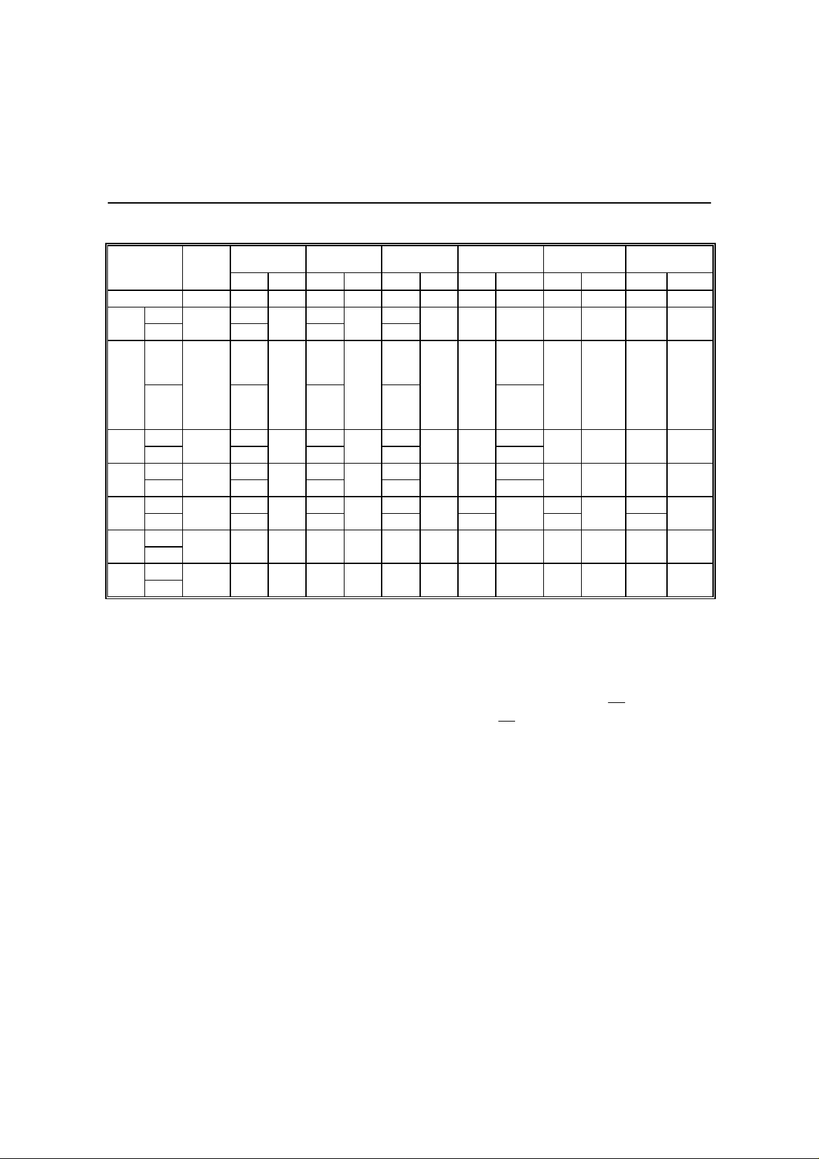
PARAMETER SYM. DESCRIPTION -90 -120 -150 UNIT
JEDEC Standard
t
AVAV
t
AVWL
t
WLAX
t
DVWH
t
WHDX
t
GHWL
t
ELWL
t
WHEH
t
WLWH
t
WHWL
t
WHWH1
t
WHWH2
t
WHWH3
Notes:
1. Not 100% tested.
2. Does not include pre-programming time.
3. This timing is for Temporary Sector Unprotect operation.
These timings are for Sector Protect and/or Sector Unprotect operations.
t
WC
t
AS
t
AH
t
DS
t
DH
t
OES
t
OEH
t
GHWL
t
CS
t
CH
t
WP
t
WPH
t
WHWH1
t
WHWH2
t
WHWH3
t
VCS
t
VIDR
t
OESP
t
RP
t
RSP
t
BUSY
t
VLHT
t
WPP1
t
WPP2
t
CSP
Write Cycle Time
Address Setup Time
Address Hold Time
Data Setup Time
Data Hold Time
Output Enable Setup Time
Output Enable Read
Hold Time
Read Recover Time Before Write
Setup Time
CE
Hold Time
CE
Write Pulse Width
Write Pulse Width High
Byte Programming Operation
Sector Erase Operation
Chip Erase Operation
Vcc Setup Time
Rise Time to VID
Setup Time to WE Active
OE
RESET
RESET
Programming/Erase Valid to RY/BY Delay
Voltage Transition Time
Sector Protect Write Pulse Width
Sector Unprotect Write Pulse Width
Setup Time to WE Active
CE
(1)
(1)
(1,3)
Pulse Width
Setup Time
(1)
Toggle &
(2)
(2)
( 3)
(1, 4)
Data
(1, 3, 4)
(4)
(1, 4)
Polling
(4)
(1)
(1)
Min.
Min.
Min.
Min.
Min.
Min.
Min.
Min.
Min.
Min.
Min.
Min.
Min.
Typ.
Max.
Typ.
Max.
Typ.
Max.
Min.
Min.
Min.
Min.
Min.
Min. 40
Min. 4
Min. 100 100 100 mS
Min. 350 350 350 mS
Min. 4
90 120 150
0
45
45
10
45
20
16
400
0.26
12
2.0
90
50
500 500 500 nS
500 500 500 nS
0
50
50
0
0
0
0
0
0
10
0
0
0
0
0
0
50
20
16
400
0.26
12
2.0
90
50
4
4
4
4
50
4
4
0
50
50
0
0
0
10
0
0
0
50
20
16
400
0.26
12
2.0
90
50
4
4
60
4
4
nS
nS
nS
nS
nS
nS
nS
nS
nS
nS
nS
nS
nS
S
µ
S
µ
sec
sec
mS
mS
S
µ
nS
mS
nS
- 24 -
Page 25

BRIGHT BM29F400T/BM29F400B
Microelectronics
Inc.
SWITCHING WAVEFORMS
WAVEFORM INPUT OUTPUT
Must Be Steady Will Be Steady
Address
CE
OE
May Change
from H to L
May Change
from L to H
Don't Care,
Any Change
Permitted
Does Not
Apply
Will Be Change
from H to L
Will Be Change
from L to H
Change,
State Unknown
Center Line is
High impedance
Off State
RC
t
Address Stable
ACC
t
HZ
OE
t
OEH
t
t
DF
t
OH
WE
Outputs
High Z
CE
t
Output Vaild
t
High Z
Figure 8. AC Waveforms for Read Operations
A Winbond Company Publication Release Date: December 1999
- 25 - Revision A2
Page 26

BRIGHT BM29F400T/BM29F400B
Microelectronics
Inc.
Switching Waveforms, continued
Data Polling
Address
CE
OE
WE
Data
5.0V
V
CC
5555H
WC
t
t
CS
GHWL
t
WP
t
A0H
PA
AS
t
WPH
t
DH
t
DS
t
GND
Figure 9. AC Waveforms Program Operations
Notes:
1. PA is address of the memory location to be programmed.
2. PD is data to be programmed at BYTE address.
3.
is the output of the complement of the data written to the device.
DQ7
4. DOUT is the output of the data written to the device.
5. Figure indicates last two bus cycles of four bus cycle sequence.
6. These waveforms are for 16-bit mode.
AS
Address
t
5555H
AH
t
2AAAH
5555H
PA
AH
t
WHWH1
t
PD
DQ7
OUT
D
5555H
2AAAH
SA
CE
GHWL
t
OE
WP
t
VCC
5.0V
GND
WE
Data
CS
t
VCS
t
WPH
t
DH
t
AAH
DS
t
55H
80H
AAH
Figure 10. AC Waveforms Chip/Sector Erase Operations
Notes:
1. SA is the sector address for Sector Erase. Address = X = Don't Care for Chip Erase.
2. These waveforms are for 16-bit mode.
- 26 -
55H
10H/30H
Page 27

BRIGHT BM29F400T/BM29F400B
Microelectronics
Inc.
Switching Waveforms, continued
CH
t
VCC
CE
OE
WE
DQ7
Data
DQ0-DQ6
5.0V
GND
Figure 11. AC Waveforms for
OEH
t
CE
t
t
Data
OE
t
DQ7 DQ7=Valid Data
WHWH 1 or 2
DQ0-DQ6=Invalid
Polling during Internal Algorithm Operations
Note: DQ7 = Valid Data (The device has completed the internal program or erase operation.)
CE
OEH
OE
t
t
OE
OH
t
DQ0-DQ7
Valid Data
DF
t
High
Z
OES
t
WE
Data
Data
(DQ0-DQ7)
DQ6=Toggle
DQ6=Toggle
OE
t
DQ6=
Stop Toggling
DQ0-DQ7
Valid
5.0V
V
CC
GND
Figure 12 AC Waveforms for Toggle Bit during Internal Algorithm Operation
Note: DQ6 stops toggling (The device has completed the internal program or erase operation.)
A Winbond Company Publication Release Date: December 1999
- 27 - Revision A2
Page 28

BRIGHT BM29F400T/BM29F400B
Microelectronics
Inc.
Switching Waveforms, continued
CE
Vcc
GND
WE
BY/RY
5.0V
RY/BY
RESET
The rising edge of the last WE signal
Entire programming
or erase operations
t
BUSY
Figure 13. RY/BY Timing Diagram During Program/Erase Operation
PWH
RP
Ready
t
Vcc
Data
5.0V
GND
Figure 14.
RESET
- 28 -
Vaild Data
Timing Diagram
Page 29

BRIGHT BM29F400T/BM29F400B
Microelectronics
Inc.
Switching Waveforms, continued
tWC
Address
Address Stable
CE
OE
BYTE
Data
(DQ0-DQ7)
Data
(DQ8-DQ14)
DQ15/A-1
tAVFL
Figure 15.
tELFL
tOE
tCE
Data Output
on DQ0-DQ7
ACC
t
Data
Outputon
DQ8-DQ14
tFLQZ
Data
Outputon
DQ15
Timing Diagram for Read Operation
BYTE
High Z
tACC
Data Output
on DQ0-DQ7
Address
Input
tDF
tOH
High Z
High Z
High Z
CE
WE
The falling edge of the last WE signal
BYTE
t
SET
Figure 16.
( )
t
AS
Timing Diagram for Write Operation
BYTE
t
HOLD
( )
tAH
A Winbond Company Publication Release Date: December 1999
- 29 - Revision A2
Page 30

BRIGHT BM29F400T/BM29F400B
Microelectronics
Inc.
Start
RESET = V
Perform Erase or
Program Operations
RESET = V
Temporary Sector
Unprotect Completed
Figure 17. Temporary Sector Unprotect Algorithm
Notes:
1. All protected sector groups unprotected.
2. All previously protected sector groups are protected again.
12V
RESET
(Note 1)
(Note 2)
ID
IH
5V
CE
WE
RY/BY
t
VIDR
t
RSP
Program or Erase Command Sequence
Figure 18. Temporary Unprotect Timing Diagram
- 30 -
Page 31

BRIGHT BM29F400T/BM29F400B
Microelectronics
Inc.
AC CHARACTERISTICS
Programming/Erase Operations
PARAMETER SYM. DESCRIPTION
JEDEC
t
AVAV
t
tAS Address Setup Time Min. 0 0 0 nS
AVEL
t
tAH Address Hold Time Min. 45 50 50 nS
ELAX
t
tDS Data Setup Time Min. 45 50 50 nS
DVEH
t
EHDX
t
t
Hold Time
t
t
GHWL
t
tWS
WLEL
t
tWH
EHWH
t
tCP
ELEH
t
t
EHEL
t
WHWH1
Max. 400 400 400 mS
t
WHWH2
Max. 12 12 12 sec
t
WHWH3
Max. 90 90 90 sec
t
t
t
t
t
t
t
Notes
:
1. Not 100% tested.
2. Does not include pre-programming time.
3. This timing is for Sector Unprotect operation.
4. Output Driver Disable Time.
Standard
tWC Write Cycle Time
tDH Data Hold Time Min. 0 0 0 nS
OES
OEH
GHWL
CPH
t
t
t
WHWH1
WHWH2
WHWH3
VCS
VIDR
VLHT
WPP1
WPP2
OESP
CSP
(1)
Min. 90 120 150 nS
Output Enable Setup Time
Output Enable Read
Read Recover Time Before Write Min. 0 0 0 nS
WE Setup Time
Hold Time
WE
Pulse Width
CE
Vcc Setup Time
Rise Time to VID
Voltage Transition Time
Sector Protect Write Pulse Width
Sector Unprotect Write Pulse Width
Pulse Width High
CE
Byte Programming Operation Typ. 16 16 16 mS
Sector Erase Operation
Chip Erase Operation
(1,3)
(1,3)
Setup Time toWEActive
OE
Setup Time toWEActive
OE
(1)
Min. 0 0 0 nS
(1)
Min. 0 0 0 nS
Toggle and
(2)
Min. 50 50 50 mS
Min. 500 500 500 nS
Data
(2)
Typ. 0.26 0.26 0.26 sec
Typ. 2.0 2.0 2.0 sec
(1,3)
Min. 4 4 4 mS
(4)
(1, 3)
(1, 4)
Polling
(4)
(1)
-90 -120 -150 Unit
Min. 10 10 10 nS
Min. 0 0 0 nS
Min. 0 0 0 nS
Min. 45 50 50 nS
Min. 20 20 20 nS
Min. 100 100 100 mS
Min. 10 10 10 mS
Min. 4 4 4 mS
Min. 4 4 4 nS
A Winbond Company Publication Release Date: December 1999
- 31 - Revision A2
Page 32

BRIGHT BM29F400T/BM29F400B
Microelectronics
Inc.
Switching Waveforms, continued
Data Polling
Address
CE
5555H
t
WC
t
GHWL
PA PA
t
AH
t
AS
OE
t
WP
WE
t
CS
t
WPH
t
D
Data
t
DS
5.0V
Vcc
GND
Figure 19. Alternate CE Controlled Program Operation Timings
Notes:
1. PA is address of the memory location to be programmed.
2. PD is data to be programmed at
3.
is the output of the complement of the data written to the device.
DQ7
BYTE
address.
4. DOUT is the output of the data written to the device.
5. Figure indicates last two bus cycles of four bus cycle sequence.
6. These waveforms are for the x16 mode.
t
WHWH1
OUT
DDQ7PDA0H
- 32 -
Page 33

BRIGHT BM29F400T/BM29F400B
Microelectronics
Inc.
Erase and Programming Performance
PARAMETER LIMITS
MIN. TYP. MAX. UNIT
Sector Erase Time 0.33 15 sec
Chip Erase Time 2.4 120 sec
Byte Programming Time 16 400
Chip Programming Time 8 200 sec
Erase/Program Cycles 10,000 100,000 cycles
Latch Up Characteristics
PARAMETER MIN. MAX.
Input Voltage with respect to Vss on all I/O
pins
Vcc Current -100 mA + 100 mA
Note: Includes all pins except Vcc. Test conditions: Vcc = 5.0V, one pin at a time.
-1.0V
Vcc + 1.0V
µ
S
CAPACITANCE
TSOP Pin
PARAMETER SYMBOL TEST SETUP TYP. MAX. UNIT
Input Capacitance
Output Capacitance
Control Pin Capacitance
Notes:
1. Sampled, not 100% tested.
2. Test conditions TA = 25°, f = 1.0 MHz.
Data Retention
PARAMETER TEST CONDITIONS MIN. UNIT
Minimum Pattern Data Retention Time
Minimum Pattern Data Retention Time
CIN
C
C
OUT
IN2
VIN = 0 6 7.5 pF
OUT
V
= 0 8.5 12 pF
VIN = 0 8 10 pF
150°
125°
10 Years
20 Years
A Winbond Company Publication Release Date: December 1999
- 33 - Revision A2
Page 34

BRIGHT BM29F400T/BM29F400B
S)
TEMPERATURE
Microelectronics
Inc.
ORDERING INFORMATION
PART NO. ACCESS
TIME
(n
29F400T-90TC
29F400T-12TC
29F400B-90TC
29F400B-12TC
Notes:
1. Winbond reserves the right to make changes to its products without prior notice.
2. Purchasers are responsible for performing appropriate quality assurance testing on products intended for use in
applications where personal injury might occur as a consequence of product failure.
3. Typical Program/Erase Cycle is 100,000.
90
120
90
120
POWER
SUPPLY
CURRENT
MAX. (mA)
60
60
60
60
BOOT
BLOCK
Top
Top
Bottom
Bottom
PACKAGE CYCLING
(MIN.)
48-pin TSOP
48-pin TSOP
48-pin TSOP
48-pin TSOP
10,000
10,000
10,000
10,000
0°C−70°C
0°C−70°C
0°C−70°C
0°C−70°C
RANGE
- 34 -
Page 35

BRIGHT BM29F400T/BM29F400B
Microelectronics
Inc.
APPENDIX A:
Compatibility to AMD's AMD29F400B:
The device is essentially fully functional compatible to the AMD29F400B except for three issues:
1. During Erase Suspend
2. DQ2 Status Flag
3. Command Address Subset
During Erase Suspend, the device can only read data in the memory-- not Program or execute an
Auto Command like the AMD29400B. Also, the DQ2 Flag is not available. This flag is used to
determine during multiple or single sector erase whether a sector has been selected for erase. DQ2
can only be used during and embedded sector erase operation or during erase suspend.
In the AMD device, commands do not require address pin A15, A14, A13, A12, A11 to be forced
during the command sequence. This makes their device slighly easier to inadvertently create a
command and cause a program, erase or malfunction. The advantage of reducing the address to a
subset is to simplify the hardware interface in systems where control signals are limited in number.
The 29F400B reduces the interface requirement by 4 signals. However if the full address is supplied
(i.e.2AAAH and 5555H) by the host system, there will be no incompatibility using either device.
A Winbond Company Publication Release Date: December 1999
- 35 - Revision A2
Page 36

BRIGHT BM29F400T/BM29F400B
Microelectronics
Inc.
PACKAGE DIMENSIONS
TSOP48
48-pin Standard Thin Small Outline Package (measured in millimeters)
0.95
1
Pin 1 I.D.
48
1.05
1.20
MAX
24
0.25MM(0.0098)BSC
18.30
18.50
19.80
20.20
11.90
12.10
25
0.08
0.20
0.10
0
5
.050
.070
0.21
0.05
0.15
0.50 BSC
- 36 -
Page 37

BRIGHT BM29F400T/BM29F400B
Microelectronics
Inc.
VERSION HISTORY
VERSION DATE PAGE DESCRIPTION
A1 May 1999 - Initial Issued
A2 Dec. 1999 1, 3, 34, 35, 37 Remove PSOP package
21, 35 Remove industrial specifications
23 Change AC Testing Input level from 0.45V/2.4V to
0V/3V and Input/Output Reference level to 1.5V
Headquarters
No. 4, Creation Rd. III,
Science-Based Industrial Park,
Hsinchu, Taiwan
TEL: 886-3-5770066
FAX: 886-3-5796096
http://www.winbond.com.tw/
Voice & Fax-on-demand: 886-2-27197006
Taipei Office
11F, No. 115, Sec. 3, Min-Sheng East Rd.,
Taipei, Taiwan
TEL: 886-2-27190505
FAX: 886-2-27197502
Note: All data and specifications are subject to change without notice.
Winbond Electronics (H.K.) Ltd.
Rm. 803, World Trade Square, Tower II,
123 Hoi Bun Rd., Kwun Tong,
Kowloon, Hong Kong
TEL: 852-27513100
FAX: 852-27552064
Winbond Electronics North America Corp.
Winbond Memory Lab.
Winbond Microelectronics Corp.
Winbond Systems Lab.
2727 N. First Street, San Jose,
CA 95134, U.S.A.
TEL: 408-9436666
FAX: 408-5441798
A Winbond Company Publication Release Date: December 1999
- 37 - Revision A2
 Loading...