

Page 1

DISCRETE SEMICONDUCTORS
DATA SH EET
BLX94C
UHF power transistor
Product specification
1996 Feb 06
Page 2

Philips Semiconductors Product specification
UHF power transistor BLX94C
FEATURES
• Withstands full load mismatch
• Emitter ballasting resistors for an optimum temperature
profile
• Gold metallization ensures excellent reliability.
APPLICATIONS
• Transmitting applications in the UHF range with a
nominal supply voltage up to 28 V.
PINNING - SOT122A
PIN SYMBOL DESCRIPTION
1 c collector
2 e emitter
3 b base
4 e emitter
QUICK REFERENCE DATA
RF performance at T
=25°C in a common emitter test circuit.
h
DESCRIPTION
NPN silicon planar epitaxial transistor primarily intended
for class-A, B or C operation. The transistor is
encapsulated in a 4-lead SOT122A stud envelope with a
ceramic cap.
handbook, halfpage
4
c
31
b
2
MAM229
e
Fig.1 Simplified outline and symbol.
MODE OF
OPERATION
f
(MHz)
V
(V)
CE
P
(W)
L
G
p
(dB)
η
(%)
C
CW, class-B 470 28 25 >6.5 >55
WARNING
Product and environmental safety - toxic materials
This product contains beryllium oxide. The product is entirely safe provided that the BeO disc is not damaged.
All persons who handle, use or dispose of this product should be aware of its nature and of the necessary safety
precautions. After use, dispose of as chemical or special waste according to the regulations applying at the location of
the user. It must never be thrown out with the general or domestic waste.
1996 Feb 06 2
Page 3
Philips Semiconductors Product specification
UHF power transistor BLX94C
LIMITING VALUES
In accordance with the Absolute Maximum Rating System (IEC 134).
SYMBOL PARAMETER CONDITIONS MIN. MAX. UNIT
V
CESM
V
CEO
V
EBO
I
C
I
C(AV)
I
CM
P
tot
T
stg
T
j
THERMAL CHARACTERISTICS
collector-emitter voltage (peak value) VBE=0 − 65 V
collector-emitter voltage open base − 30 V
emitter-base voltage open collector − 4V
collector current (DC) − 2.5 A
average collector current − 2.5 A
peak collector current f > 1 MHz − 6A
total power dissipation ≤ Tmb=25°C − 60 W
storage temperature −65 +150 °C
operating junction temperature − 200 °C
SYMBOL PARAMETER CONDITIONS VALUE UNIT
R
th j-mb
thermal resistance from junction to
P
=20W;Tmb=82°C; Th=70°C 4 K/W
tot
mounting base (DC dissipation)
R
th j-mb
thermal resistance from junction to
P
=20W;Tmb=82°C; Th=70°C 2.7 K/W
tot
mounting base (RF dissipation)
R
th mb-h
thermal resistance from mounting base
P
=20W;Tmb=82°C; Th=70°C 0.6 K/W
tot
to heatsink
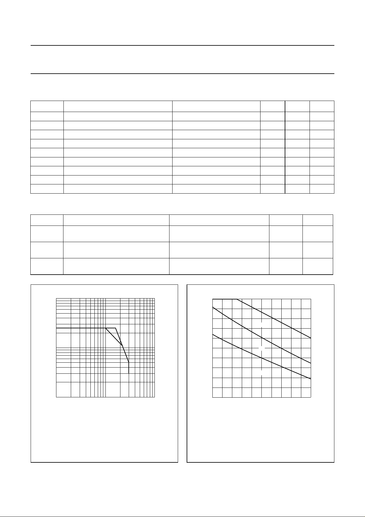
10
handbook, halfpage
I
C
(A)
1
−1
10
11010
(1)(2)
VCE (V)
MBH096
2
60
handbook, halfpage
P
tot
(W)
50
40
30
20
10
0 100
(3)
(2)
(1)
50 Th (
MBH097
o
C)
(1) Tmb=25°C.
(2) Th=70°C.
Fig.2 DC SOAR.
1996 Feb 06 3
(1) Continuous DC operation.
(2) Continuous RF operation.
(3) Short-time operation during mismatch.
Fig.3 Power derating curves.
Page 4
Philips Semiconductors Product specification
UHF power transistor BLX94C
CHARACTERISTICS
T
=25°C unless otherwise specified.
j
SYMBOL PARAMETER CONDITIONS MIN. TYP. MAX. UNIT
V
(BR)CES
V
(BR)CEO
V
(BR)EBO
V
CEsat
I
CES
E
SBR
h
FE
f
T
C
c
C
re
C
c-s
collector-emitter breakdown voltage VBE= 0; IC=25mA 65 −−V
collector-emitter breakdown voltage open base; IC= 100 mA 30 −−V
emitter-base breakdown voltage open collector; IE=10mA 4 −−V
collector-emitter saturation voltage IC= 4 A; IB= 0.8 A; note 1 − 1.5 − V
collector cut-off current VBE= 0; VCE=30V −−10 mA
second breakdown energy open base; L = 25 mH; f = 50 Hz 3 −−mJ
=10Ω; L = 25 mH; f = 50 Hz 3 −−mJ
R
BE
DC current gain VCE=5V; IC= 1.5 A; note 1 15 50 −
transition frequency VCB= 28 V; IE= −1.5 A;
− 1.1 − f
T
f = 500 MHz; note 1
VCB= 28 V; IE= −4A;
− 0.75 − f
T
f = 500 MHz; note 1
collector capacitance VCB= 28 V; IE=ie= 0; f = 1 MHz − 33 − pF
feedback capacitance VCE= 28 V; IC= 20 mA; f = 1 MHz; − 18 − pF
collector-stud capacitance − 1.2 − pF
Note
1. Measured under pulsed conditions: t
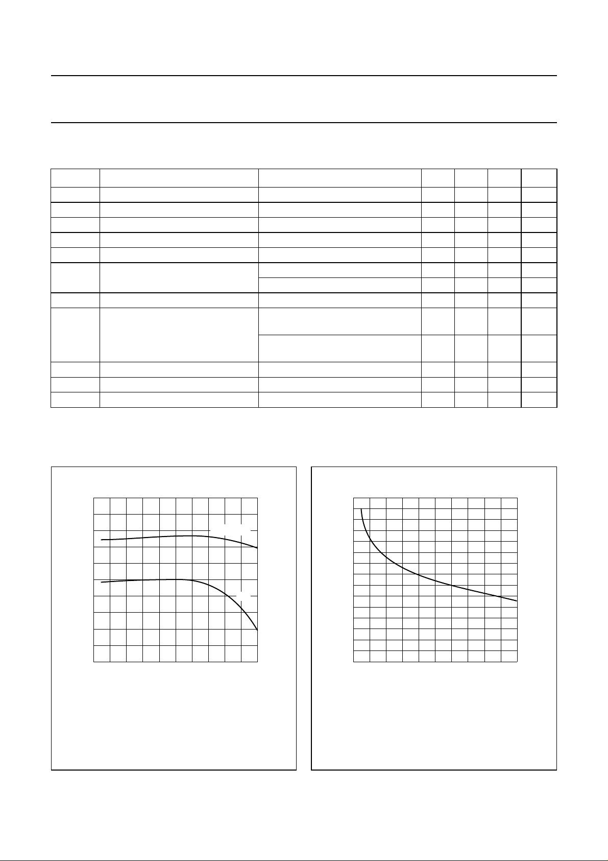
100
handbook, halfpage
h
FE
50
0
04
Measured under pulsed conditions; tp≤ 200 µs; δ≤0.02;Tj=25°C.
(1) VCE=25V.
(2) VCE=5V.
2I
≤ 200 µs; δ≤0.02.
p
MBH099
VCE = 25 V
5 V
(A)
C
75
handbook, halfpage
C
c
(pF)
50
25
0
040
IE=ie= 0; f = 1 MHz; Tj=25°C.
MBH098
20 VCB (V)
Fig.4 DC current gain as a function of collector
current; typical values.
1996 Feb 06 4
Fig.5 Collector capacitance as a function of
collector-base voltage; typical values.
Page 5

Philips Semiconductors Product specification
UHF power transistor BLX94C
1,5
handbook, full pagewidth
f
T
(GHz)
1
0.5
0
0
VCB= 28 V; Tj=25°.
−1 −2
−3I
E
Fig.6 Transmission frequency as a function of emitter current; typical values.
(A)
MBH106
−4
1996 Feb 06 5
Page 6

Philips Semiconductors Product specification
UHF power transistor BLX94C
APPLICATION INFORMATION
RF performance at T
=25°C in a common emitter, class-B test circuit.
h
MODE OF OPERATION
CW, class-B 470 28 25 <5.6
10
handbook, halfpage
G
p
(dB)
5
0
040
VCE=28V.
ICQ= 200 mA.
f = 470 MHz.
f
(MHz)
G
p
η
20 PL (W)
MBH101
V
(V)
CE
100
(%)
50
0
P
L
(W)
handbook, halfpage
η
P
S
(W)
typ. 4.7
40
P
L
(W)
30
20
10
0
024 8
VCE=28V.
Th=25°C.
f = 470 MHz.
G
p
(dB)
>6.5
typ. 7.25
I
C
(A)
<1.62
typ. 1.54
6
MBH100
PS (W)
η
C
(%)
>55
typ. 58
Fig.7 Power gain and efficiency as functions of
load power; typical values.
1996 Feb 06 6
Fig.8 Load power as a function of source power;
typical values.
Page 7

Philips Semiconductors Product specification
UHF power transistor BLX94C
handbook, full pagewidth
input
ZS = 50 Ω
C2
C1
L1
T.U.T.
+V
L3
C5
R2
L5
CC
R1
C4C3
L2
C7
L4
C8
C6
output
ZL = 50 Ω
MBH107
Fig.9 Class-B test circuit at f = 470 MHz.
List of components (see Figs 9 and 10)
COMPONENT DESCRIPTION VALUE DIMENSIONS
CATALOGUE
No.
C1, C2, C8 film dielectric trimmer capacitor 2 to 9 pF 2222 809 09002
C3, C4 chip capacitor 15 pF
C5 feed through capacitor 100 pF
C6 polyester capacitor 33 nF
C6 chip capacitor 22 nF, 63 V
C7 film dielectric trimmer capacitor 2 to 18 pF 2222 809 09003
L1 stripline; note 1 length 41.1 mm
width 5 mm
L2 13 turns enamelled 0.5 mm copper
wire
int. diameter 4 mm
close wound
L3 2 turns 1 mm copper wire int. diameter 4 mm
winding pitch 1.5 mm
leads 2 x 5 mm
L4 stripline; note 1 length 52.7 mm
width 5 mm
L5 Ferroxcube choke coil 750 Ω; ± 20% 4312 020 36640
R1 carbon resistor 1 Ω
R2 carbon resistor 10 Ω
Note
1. The striplines are on double-clad PCB with PTFE fibre-glass dielectric (ε
1996 Feb 06 7
= 2.74); thickness 1.45 mm.
r
Page 8

Philips Semiconductors Product specification
UHF power transistor BLX94C
handbook, full pagewidth
input
50 Ω
C1
C2
146
52.741.1
rivet (4x)
47
L2
R1
L1
C4
C3
C7
L4
L3
C5
C6
R2
L5
C8
V
CC
output
50 Ω
MBH108
Dimensions in mm.
The components are located on one side of the copper-clad PTFE microfibre-glass board, the other side is unetched and serves as a ground plane.
Earth connections from the component side to the ground plane are made by through metallization.
Fig.10 Component layout and printed-circuit board for 470 MHz class-B test circuit.
1996 Feb 06 8
Page 9

Philips Semiconductors Product specification
UHF power transistor BLX94C
30
handbook, halfpage
P
L
(W)
20
10
1 10 VSWR
VCE= 28 V; f = 470 MHz; R
th mb-h
= 0.6 K/W.
Fig.11 Load power as a function of VSWR.
Th = 50
MBH102
o
C
o
70
o
90
handbook, halfpage
C
C
2
10
3
ri, x
i
(Ω)
2
1
r
i
0
−1
−2
100 500
VCE= 28 V; PL=25W;
=25°C; Class-B operation.
T
h
300 f (MHz)
MBH103
x
i
Fig.12 Input impedance as a function of frequency
(series components); typical values.
8
handbook, halfpage
RL, X
L
(Ω)
X
L
6
R
L
4
100 500
VCE= 28 V; PL=25W;
=25°C; Class-B operation.
T
h
300 f (MHz)
MBH104
Fig.13 Load impedance as a function of frequency
(series components); typical values.
24
handbook, halfpage
G
p
(dB)
20
16
12
8
4
0
100 500
VCE= 28 V; PL=25W;
=25°C; Class-B operation.
T
h
300 f (MHz)
Fig.14 Power gain as a function of frequency;
typical values.
MBH105
1996 Feb 06 9
Page 10

Philips Semiconductors Product specification
UHF power transistor BLX94C
PACKAGE OUTLINE
5.9
4
5.5
7.6 max
27.6
24.9
handbook, full pagewidth
27.6
24.9
3.0
Dimensions in mm.
Torque on nut: min. 0.75 Nm; max. 0.85 Nm.
Mounting hole to have no burrs at either end.
De-burring must leave surface flat; do not chamfer or countersink either end of hole.
When locking is required an adhesive is preferred instead of a lock washer.
2
(4x)
8.8
min
5
(4x)
31
8.5
MSA246
1.52
6.35
3.3
8-32 UNC
1.6
max
12.0
11.0
3.25
2.80
5.6 max
0.14
metal
BeO
ceramic
Fig.15 SOT122A.
1996 Feb 06 10
Page 11

Philips Semiconductors Product specification
UHF power transistor BLX94C
DEFINITIONS
Data Sheet Status
Objective specification This data sheet contains target or goal specifications for product development.
Preliminary specification This data sheet contains preliminary data; supplementary data may be published later.
Product specification This data sheet contains final product specifications.
Limiting values
Limiting values given are in accordance with the Absolute Maximum Rating System (IEC 134). Stress above one or
more of the limiting values may cause permanent damage to the device. These are stress ratings only and operation
of the device at these or at any other conditions above those given in the Characteristics sections of the specification
is not implied. Exposure to limiting values for extended periods may affect device reliability.
Application information
Where application information is given, it is advisory and does not form part of the specification.
LIFE SUPPORT APPLICATIONS
These products are not designed for use in life support appliances, devices, or systems where malfunction of these
products can reasonably be expected to result in personal injury. Philips customers using or selling these products for
use in such applications do so at their own risk and agree to fully indemnify Philips for any damages resulting from such
improper use or sale.
1996 Feb 06 11
 Loading...