

Page 1

DISCRETE SEMICONDUCTORS
DATA SH EET
BLW96
HF/VHF power transistor
Product specification
August 1986
Page 2
Philips Semiconductors Product specification
HF/VHF power transistor BLW96
DESCRIPTION
N-P-N silicon planar epitaxial
transistor intended for use in class-A,
AB and B operated high power
industrial and military transmitting
conditions. Transistors are supplied
in matched h
groups.
FE
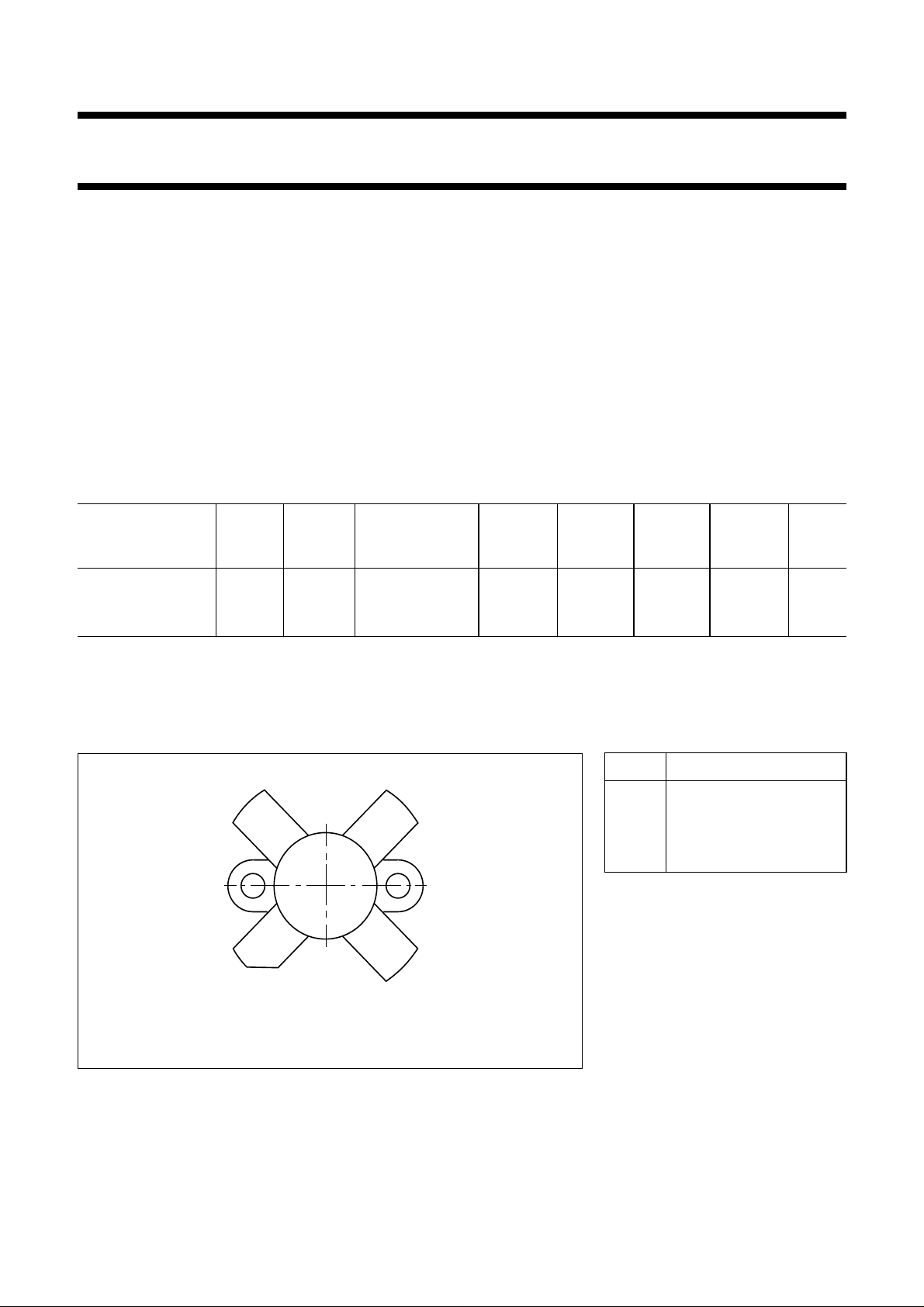
The transistor has a1⁄2" flange
envelope with a ceramic cap. All
leads are isolated from the flange.
equipment in the h.f. and v.h.f. band.
The transistor presents excellent
performance as a linear amplifier in
s.s.b. applications. It is resistance
stabilized and is guaranteed to
withstand severe load mismatch
QUICK REFERENCE DATA
R.F. performance up to T
=25°C
h
I
MODE OF
OPERATION
s.s.b. (class-AB) 50 1,6 − 28 25 − 200 (P.E.P.) > 13,5 > 40
V
CE
V
f
MHz
P
W
L
G
p
dB
%
η
(1)
d
dB
3
d
dB
5
<−30 <−30 0,1
c.w. (class-B) 50 108 200 typ. 6,5 typ. 67 −−(6)
s.s.b. (class-A) 40 28 50 (P.E.P.) typ. 19 − typ. −40 <−40 (4)
Note
1. η
at 200 W P.E.P.
dt
C(ZS)
(IC)
A
PIN CONFIGURATION
PINNING - SOT121B.
PIN DESCRIPTION
handbook, halfpage
43
1 collector
2 emitter
3 base
4 emitter
21
MLA876
Fig.1 Simplified outline. SOT121B.
PRODUCT SAFETY This device incorporates beryllium oxide, the dust of which is toxic. The device is entirely
safe provided that the BeO disc is not damaged.
August 1986 2
Page 3
Philips Semiconductors Product specification
HF/VHF power transistor BLW96
RATINGS
Limiting values in accordance with the Absolute Maximum System (IEC 134)
Collector-emitter voltage (V
peak value V
Collector-emitter voltage (open base) V
Emitter-base voltage (open collector) V
Collector current (average) I
Collector current (peak value); f > 1 MHz I
R.F. power dissipation (f > 1 MHz); T
Storage temperature T
Operating junction temperature T
BE
=0)
CESM
CEO
EBO
C(AV)
CM
=45°CP
mb
rf
stg
j
max. 110 V
max. 55 V
max. 4 V
max. 12 A
max. 40 A
max. 340 W
−65 to + 150 °C
max. 200 °C
2
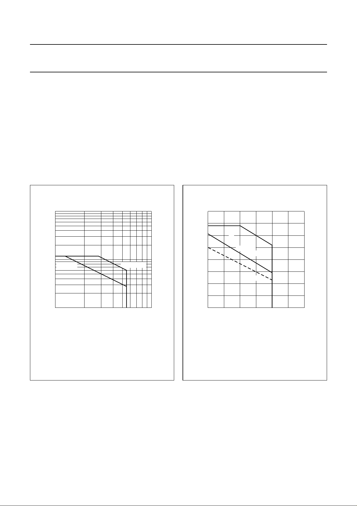
10
handbook, halfpage
I
C
(A)
10
Th = 70 °C
1
10 10
Fig.2 D.C. SOAR.
MGP685
Tmb = 45 °C
VCE (V)
400
handbook, halfpage
P
tot
(W)
300
200
100
2
0
0 50 100 150
I Continuous d.c. operation
II Continuous r.f. operation; f >1 MHz
III Short-time operation during mismatch; f > 1 MHz
ΙΙΙ
derate by
1.58 W/K
ΙΙ
Ι
1.35 W/K
MGP686
Th (°C)
Fig.3 Power/temperature derating curves.
THERMAL RESISTANCE
(dissipation = 150 W; T
= 100 °C, i.e. Th=70°C)
mb
From junction to mounting base (d.c. dissipation) R
From junction to mounting base (r.f. dissipation) R
From mounting base to heatsink R
August 1986 3
th j-mb(dc)
th j-mb(rf)
th mb-h
= 0,63 K/W
= 0,45 K/W
= 0,2 K/W
Page 4

Philips Semiconductors Product specification
HF/VHF power transistor BLW96
CHARACTERISTICS
T
=25°C
j
Collector-emitter breakdown voltage
V
=0;IC=50mA V
BE
Collector-emitter breakdown voltage
open base; IC= 200 mA V
Emitter-base breakdown voltage
open collector; IE=20mA V
Collector cut-off current
VBE=0;VCE=55V I
Second breakdown energy; L = 25 mH; f = 50 Hz
open base E
R
=10Ω E
BE
D.C. current gain
(1)
IC= 7 A; VCE=5 V h
(BR)CES
(BR)CEO
(BR)EBO
CES
SBO
SBR
FE
> 110 V
> 55 V
> 4V
< 10 mA
> 20 mJ
> 20 mJ
typ.
15 to3050
D.C. current gain ratio of matched devices
(1)
IC= 7 A; VCE=5V h
Collector-emitter saturation voltage
(1)
IC= 20 A; IB = 4 A V
Transition frequency at f = 100 MHz
(2)
−IE= 7 A; VCB= 45 V f
= 20 A; VCB= 45 V f
−I
E
Collector capacitance at f = 1 MHz
IE=Ie= 0; VCB=50V
Feedback capacitance at f = 1 MHz C
I
= 150 mA; VCE=50V C
C
Collecting-flange capacitance C
Notes
1. Measured under pulse conditions: t
≤ 300 µs; δ≤0,02.
p
2. Measured under pulse conditions: tp≤ 50 µs; δ≤0,01.
FE1/hFE2
CEsat
T
T
c
re
cf
≤ 1,2
typ. 1,9 V
typ. 235 MHz
typ. 245 MHz
typ. 280 pF
typ. 170 pF
typ. 4,4 pF
August 1986 4
Page 5

Philips Semiconductors Product specification
HF/VHF power transistor BLW96
10
handbook, halfpage
−I
E
(A)
1
−1
10
−2
10
MGP687
Th = 70 °C
25 °C
VBE (mV)
Fig.4 Typical values; VCE= 40 V.
50
handbook, halfpage
h
FE
40
30
20
10
1250500 1000750
0
010
VCE = 45 V
20
MGP688
15 V
5 V
(A)
30
I
C
Fig.5 Typical values; Tj=25°C.
300
handbook, halfpage
f
T
(MHz)
200
100
0
0 102030
VCB = 45 V
15 V
5 V
MGP689
−IE (A)
Fig.6 Typical values; f = 100 MHz; Tj=25°C.
August 1986 5
1000
handbook, halfpage
C
c
(pF)
750
500
250
0
0 255075
Fig.7 IE=Ie= 0; f = 1 MHz; Tj=25°C.
MGP690
typ
VCB (V)
Page 6

Philips Semiconductors Product specification
HF/VHF power transistor BLW96
APPLICATION INFORMATION
R.F. performance in s.s.b. class-AB operation (linear power amplifier)
V
= 50 V; Th=25°C; f1= 28,000 MHz; f2 = 28,001 MHz
CE
OUTPUT POWER G
p
ηdt (%) IC(A) d
(1)
3
W dB at 200 W (P.E.P.) dB dB A
25 to 200 (P.E.P.) > 13,5 > 40 < 5,0 <−30 < −30 0,1
(1)
d
5
I
C(ZS)
L3
C10
C11
C12 C13
+V
CC
handbook, full pagewidth
50 Ω
C1
C2
L1 R1
C4
C3
temperature
compensated bias
(Ri < 0.1 Ω)
L4
T.U.T.
L2
R2
C5
C6
C7
C8
C9
Fig.8 Test circuit; s.s.b. class-AB.
List of components:
C1 = C4 = C10 = C14 = 100 pF film dielectric trimmer
C2 = 27 pF ceramic capacitor (500 V)
C3 = 270 pF polysterene capacitor (630 V)
C5 = C7 = C8 = 220 nF multilayer ceramic chip capacitor
(2)
C6 = 27 pF multilayer ceramic chip capacitor (500 V; ATC
)
C9 = 47 µF/63 V electrolytic capacitor
(2)
)
(2)
) in parallel
(2)
) in parallel
C11 = 2 × 36 pF multilayer ceramic chip capacitors (500 V; ATC
C12 = 2 × 43 pF multilayer ceramic chip capacitors (500 V; ATC
C13 = 43 pF multilayer ceramic chip capacitor (500 V; ATC
L1 = 88 nH; 3 turns Cu wire (1,0 mm); int. dia. 9,0 mm; length 6,1 mm; leads 2 × 5 mm
L2 = Ferroxcube wide-band h.f. choke, grade 3B (cat. no. 4312 020 36640)
L3 = 150 nH; 5 turns Cu wire (2,0 mm); int. dia. 10,0 mm; length 18,7 mm; leads 2 × 5 mm
L4 = 197 nH; 5 turns Cu wire (2,0 mm); int. dia. 12,0 mm; length 18,6 mm; leads 2 × 5 mm
R1 = 0,66 Ω; parallel connection of 5 × 3,3 Ω metal film resistors (PR37; ± 5%; 1,6 W each)
R2 = 27 Ω carbon resistor (± 5%; 0,5 W)
50 Ω
C14
MGP691
Notes
1. Stated intermodulation distortion figures are referred to the according level of either of the equal amplified tones.
Relative to the according peak envelope powers these figures should be increased by 6 dB.
2. ATC means American Technical Ceramics.
August 1986 6
Page 7

Philips Semiconductors Product specification
HF/VHF power transistor BLW96
−25
handbook, halfpage
d3, d
5
(dB)
−35
−45
0 100 200 300
VCE= 50 V; I
= 28,001 MHz; Th=25°C; typical values.
f
2
d
3
d
5
= 0,1 A; f1= 28,000 MHz;
C(ZS)
MGP692
P.E.P. (W)
Fig.9 Intermodulation distortion as a function of
output power.
(1)
100
handbook, halfpage
η
dt
(%)
G
75
50
25
0
0 100
VCE= 50 V; I
= 28,001 MHz; Th=25°C; typical values.
f
2
p
η
dt
= 0,1 A; f1= 28,000 MHz;
C(ZS)
200
MGP693
P.E.P. (W)
Fig.10 Double-tone efficiency and power gain as a
function of output power.
300
20
15
10
5
0
G
(dB)
p
Ruggedness
The BLW96 is capable of withstanding full load mismatch
(VSWR = 50 through all phases) up to 150 W (P.E.P.) or a
load mismatch (VSWR = 5 through all phases) up to
200 W (P.E.P.) under the following conditions:
VCE= 45 V; f = 28 MHz; Th=70°C; R
th mb-h
= 0,2 K/W.
August 1986 7
Page 8

Philips Semiconductors Product specification
HF/VHF power transistor BLW96
30
handbook, halfpage
G
p
(dB)
20
10
0
11010
VCE= 50 V; I
=25°C; ZL=5Ω; neutralizing capacitor: 47 pF
T
h
= 0,1 A; PL= 200 W (P.E.P.);
C(ZS)
f (MHz)
Fig.11 Power gain as a function of frequency.
MGP694
2
r
i
i
f (MHz)
MGP695
2
4
ndbook, halfpage
r
, −x
i
i
(Ω)
3
2
1
0
11010
VCE= 50 V; I
=25°C; ZL=5Ω; neutralizing capacitor: 47 pF
T
h
r
i
−x
i
= 0,1 A; PL= 200 W (P.E.P.);
C(ZS)
−x
Fig.12 Input impedance (series components) as a
function of frequency.
Figs 11 and 12 are typical curves and hold for one
transistor of a push-pull amplifier with cross-neutralization
in s.s.b. class-AB operation.
August 1986 8
Page 9

Philips Semiconductors Product specification
HF/VHF power transistor BLW96
R.F. performance in c.w. operation (unneutralized common-emitter class-B circuit)
T
= 25 °C
h
f (MHz) V
(V) PL(W) PS(W) Gp(dB) IC (A) η (%)
CE
108 50 200 typ. 45 typ. 6,5 typ. 6 typ. 67
PS (W)
MGP696
10
handbook, halfpage
G
p
(dB)
7.5
5
2.5
0
0 100 200 300
G
p
η
400
handbook, halfpage
P
L
(W)
300
200
100
0
0 255075
typ
PL (W)
MGP697
100
η
(%)
75
50
25
0
Fig.13 VCE= 50 V; f = 108 MHz; Th=25°C.
Fig.14 VCE= 50 V; f = 108 MHz; Th=25°C;
typical values.
August 1986 9
Page 10

Philips Semiconductors Product specification
HF/VHF power transistor BLW96
handbook, halfpage
1
ri, x
i
(Ω)
0.5
0
−0.5
Typical values; VCE= 50 V; PL= 200 W; Th=25°C;
class-B operation
r
i
x
i
25 125
75
f (MHz)
Fig.15 Input impedance (series components).
MGP698
handbook, halfpage
6
RL, X
L
(Ω)
R
4
2
0
25 125
Typical values; VCE= 50 V; PL= 200 W; Th=25°C;
class-B operation
L
X
L
75
f (MHz)
Fig.16 Load impedance (series components).
MGP699
20
handbook, halfpage
G
p
(dB)
10
0
25 125
Typical values; VCE= 50 V; PL= 200 W; Th=25°C;
class-B operation
75
Fig.17
MGP700
f (MHz)
August 1986 10
Page 11

Philips Semiconductors Product specification
HF/VHF power transistor BLW96
R.F. performance in s.s.b. class-A operation (linear power amplifier)
V
= 40 V; Th=25°C; f1= 28,000 MHz; f2 = 28,001 MHz
CE
OUTPUT POWER
W
G
dB
p
I
C
A
d
3
dB
(1)
typ. 50 (P.E.P.) typ. 19 4 typ. −40 < −40
d
5
dB
(1)
C8
C9
C10
50 Ω
MGP701
handbook, full pagewidth
50 Ω
C1
+V
BB
C2
L4
L1
L2
C3
C4
R1
T.U.T.
C5
C6
L3
C7
+V
CC
Fig.18 Test circuit; s.s.b. class-A.
List of components:
C1 = C2 = 10 to 780 pF film dielectric trimmer
C3 = 220 nF polyester capacitor (100 V)
C4 = 100 µF/4 V electrolytic capacitor
C5 = 2 × 330 nF polyester capacitors (100 V) in parallel
C6 = 47 µF/63 V electrolytic capacitor
C7 = C10 = 2 × 82 pF ceramic capacitors (500 V) in parallel
C8 = C9 = 10 to 150 pF air dielectric trimmer
L1 = 45 nH; 2 turns enamelled Cu wire (1,6 mm); int. dia. 8,0 mm; length 4,0 mm; leads 2 × 3 mm
L2 = Ferroxcube wide-band h.f. choke, grade 3B (cat. no. 4312 020 36640)
L3 = 110 nH; 4 turns enamelled Cu wire (2,0 mm); int. dia. 10,0 mm; length 8,0 mm; leads 2 × 2mm
L4 = 210 nH; 5 turns enamelled Cu wire (2,0 mm); int. dia. 12,0 mm; length 10,0 mm; leads 2 × 2 mm
R1 = 27 Ω carbon resistor (± 5%; 0,5 W)
Note
1. Stated intermodulation distortion figures are referred to the according level of either of the equal amplified tones.
Relative to the according peak envelope powers these figures should be increased by 6 dB.
August 1986 11
Page 12

Philips Semiconductors Product specification
HF/VHF power transistor BLW96
−30
handbook, full pagewidth
d
3
(dB)
−40
−50
−60
020 80
IC = 3 A 4 A
40 60
Fig.19 Third order intermodulation distortion as a function of output power.
Th=25°C; f1= 28,000 MHz; f2= 28,001 MHz.
5 A
P.E.P. (W)
(1)
Typical values; VCE=40V;
MGP702
100
August 1986 12
Page 13

Philips Semiconductors Product specification
HF/VHF power transistor BLW96
PACKAGE OUTLINE
Flanged ceramic package; 2 mounting holes; 4 leads SOT121B
D
A
F
H
43
α
12
H
q
U
1
L
C
B
b
p
w
M
C
2
A
U
U
2
w
M
AB
1
D
3
1
c
Q
0 5 10 mm
scale
DIMENSIONS (millimetre dimensions are derived from the original inch dimensions)
5.82
5.56
c
Db
12.83
12.86
0.16
0.10
0.006
0.004
IEC JEDEC EIAJ
12.59
0.506
0.496
12.57
0.505
0.495
F
D
1
2.67
28.45
2.41
0.105
0.095
7.93
25.52
6.32
1.120
0.312
1.005
0.249
REFERENCES
0.130
0.120
UNIT
inches
A
7.27
mm
6.17
0.229
0.286
0.219
0.243
OUTLINE
VERSION
SOT121B 97-06-28
pH
3.30
3.05
Q
4.45
3.91
0.175
0.154
q
18.42
0.725
U
1
24.90
24.63
0.98
0.97
U
6.48
6.22
0.255
0.245
2
w1w
U
3
12.32
0.51
12.06
0.485
0.02
0.475
EUROPEAN
PROJECTION
August 1986 13
2
1.02
0.04
ISSUE DATE
αL
45°
Page 14

Philips Semiconductors Product specification
HF/VHF power transistor BLW96
DEFINITIONS
Data Sheet Status
Objective specification This data sheet contains target or goal specifications for product development.
Preliminary specification This data sheet contains preliminary data; supplementary data may be published later.
Product specification This data sheet contains final product specifications.
Limiting values
Limiting values given are in accordance with the Absolute Maximum Rating System (IEC 134). Stress above one or
more of the limiting values may cause permanent damage to the device. These are stress ratings only and operation
of the device at these or at any other conditions above those given in the Characteristics sections of the specification
is not implied. Exposure to limiting values for extended periods may affect device reliability.
Application information
Where application information is given, it is advisory and does not form part of the specification.
LIFE SUPPORT APPLICATIONS
These products are not designed for use in life support appliances, devices, or systems where malfunction of these
products can reasonably be expected to result in personal injury. Philips customers using or selling these products for
use in such applications do so at their own risk and agree to fully indemnify Philips for any damages resulting from such
improper use or sale.
August 1986 14
 Loading...