

Page 1

DISCRETE SEMICONDUCTORS
DATA SH EET
BLW77
HF/VHF power transistor
Product specification
August 1986
Page 2
Philips Semiconductors Product specification
HF/VHF power transistor BLW77
DESCRIPTION
N-P-N silicon planar epitaxial
transistor intended for use in class-AB
or class-B operated high power
transmitters in the h.f. and v.h.f.
mismatch conditions. Transistors are
delivered in matched h
groups.
FE
The transistor has a1⁄2" flange
envelope with a ceramic cap. All
leads are isolated from the flange.
bands. The transistor presents
excellent performance as a linear
amplifier in the h.f. band. It is
resistance stabilized and is
guaranteed to withstand severe load
QUICK REFERENCE DATA
R.F. performance up to T
MODE OF OPERATION V
s.s.b. (class-AB) 28 0,1 1,6 − 28 15 − 130
= 25 °C
h
V
CE
I
C(ZS)
A
f
MHz
P
W
L
G
p
dB
> 12 > 37,5
%
η
(1)
<−30
(P.E.P.)
c.w. (class-B) 28 − 87,5 130 typ. 7,5 typ. 75 −
Note
1. At 130 W P.E.P.
d
dB
3
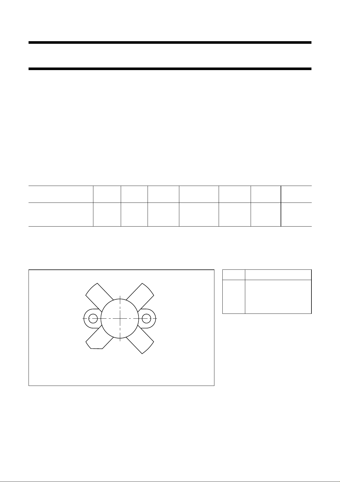
PIN CONFIGURATION
PINNING - SOT121B.
PIN DESCRIPTION
handbook, halfpage
43
1 collector
2 emitter
3 base
4 emitter
21
MLA876
Fig.1 Simplified outline. SOT121B.
PRODUCT SAFETY This device incorporates beryllium oxide, the dust of which is toxic. The device is entirely
safe provided that the BeO disc is not damaged.
August 1986 2
Page 3
Philips Semiconductors Product specification
HF/VHF power transistor BLW77
RATINGS
Limiting values in accordance with the Absolute Maximum System (IEC 134)
Collector-emitter voltage (V
peak value V
Collector-emitter voltage (open base) V
Emitter-base voltage (open collector) V
Collector current (average) I
Collector current (peak value); f > 1 MHz I
R.F. power dissipation (f > 1 MHz;); T
Storage temperature T
Operating junction temperature T
BE
= 0)
CESM
CEO
EBO
C(AV)
CM
= 25 °CP
mb
rf
stg
j
max. 70 V
max. 35 V
max. 4 V
max. 12 A
max. 30 A
max. 245 W
−65 to + 150 °C
max. 200 °C
2
10
handbook, halfpage
I
C
(A)
10
1
11010
Th = 70 °C
Fig.2 D.C. SOAR.
Tmb = 25 °C
VCE (V)
MGP521
2
300
handbook, halfpage
P
rf
(W)
200
100
0
0
I Continuous d.c. operation
II Continuous r.f. operation
III Short-time operation during mismatch
ΙΙΙ
ΙΙ
Ι
derate by 1.11 W/K
derate by 0.82 W/K
50 100
Th (°C)
MGP522
Fig.3 R.F. power dissipation; VCE≤ 28 V; f ≥ 1 MHz.
THERMAL RESISTANCE
(dissipation = 100 W; T
=90°C, i.e. Th=70°C)
mb
From junction to mounting base (d.c. dissipation) R
From junction to mounting base (r.f. dissipation) R
From mounting base to heatsink R
August 1986 3
th j-mb(dc)
th j-mb(rf)
th mb-h
= 1,03 K/W
= 0,71 K/W
= 0,2 K/W
Page 4
Philips Semiconductors Product specification
HF/VHF power transistor BLW77
CHARACTERISTICS
T
=25°C unless otherwise specified
j
Collector-emitter breakdown voltage
V
= 0; IC= 50 mA V
BE
Collector-emitter breakdown voltage
open base; IC= 100 mA V
Emitter-base breakdown voltage
open collector; IE= 20 mA V
Collector cut-off current
VBE= 0; VCE= 35 V I
D.C. current gain
(1)
IC= 7 A; VCE=5 V h
D.C. current gain ratio of matched devices
(1)
IC= 7 A; VCE=5 V h
Collector-emitter saturation voltage
(1)
IC= 20 A; IB=4 A V
Transition frequency at f = 100 MHz
(2)
−IE= 7 A; VCB= 28 V f
−I
= 20 A; VCB= 28 V f
E
Collector capacitance at f = 1 MHz
I
= 0; VCB= 28 V C
E=Ie
Feedback capacitance at f = 1 MHz
IC= 100 mA; VCE= 28 V C
Collector-flange capacitance C
(BR) CES
(BR) CEO
(BR)EBO
CES
FE
FE1/hFE2
CEsat
T
T
c
re
cf
> 70 V
> 35 V
> 4V
< 20 mA
15 to 80
< 1,2
typ. 2 V
typ. 320 MHz
typ. 300 MHz
typ. 255 pF
typ. 175 pF
typ. 3 pF
Notes
1. Measured under pulse conditions: t
≤ 300 µs; δ≤0,02.
p
2. Measured under pulse conditions: tp≤ 50 µs; δ≤0,01.
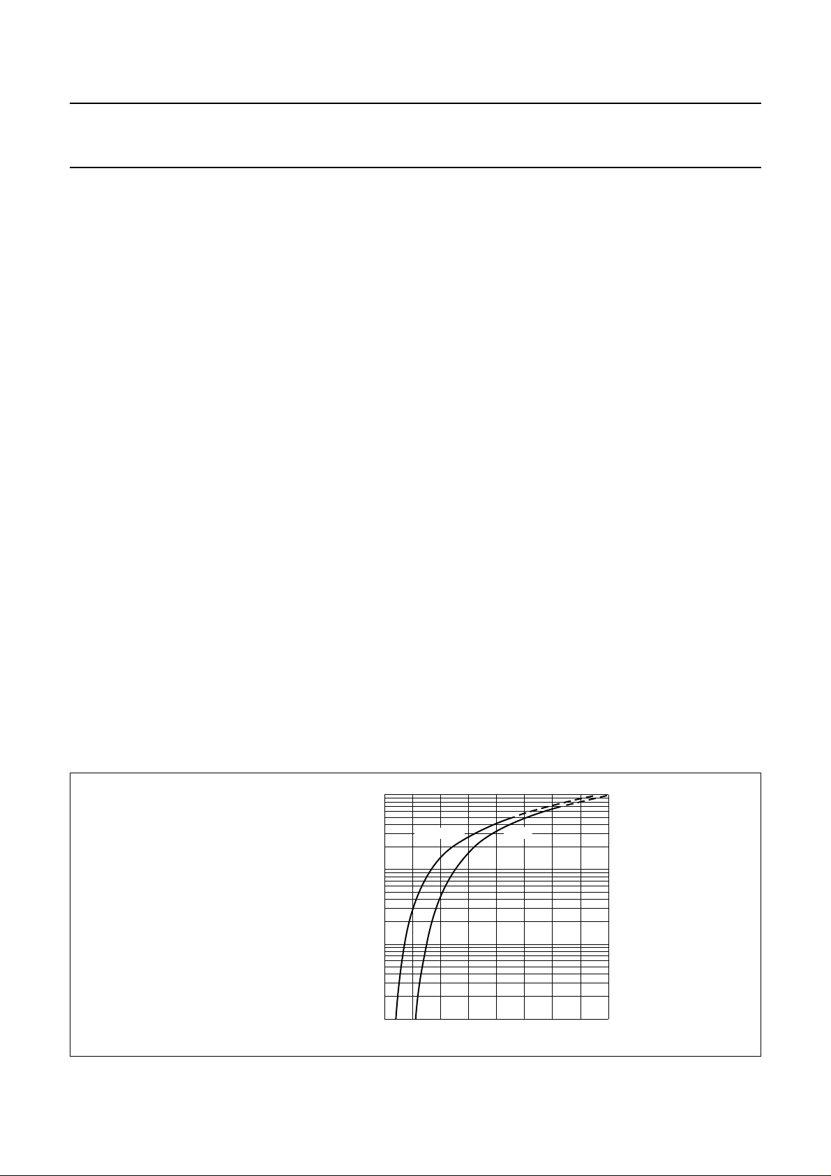
10
handbook, halfpage
I
C
(A)
1
−1
10
−2
10
Fig.4 Typical values; VCE= 20 V.
August 1986 4
Th = 70 °C
25 °C
VBE (V)
MGP523
1.50.5 1
Page 5
Philips Semiconductors Product specification
HF/VHF power transistor BLW77
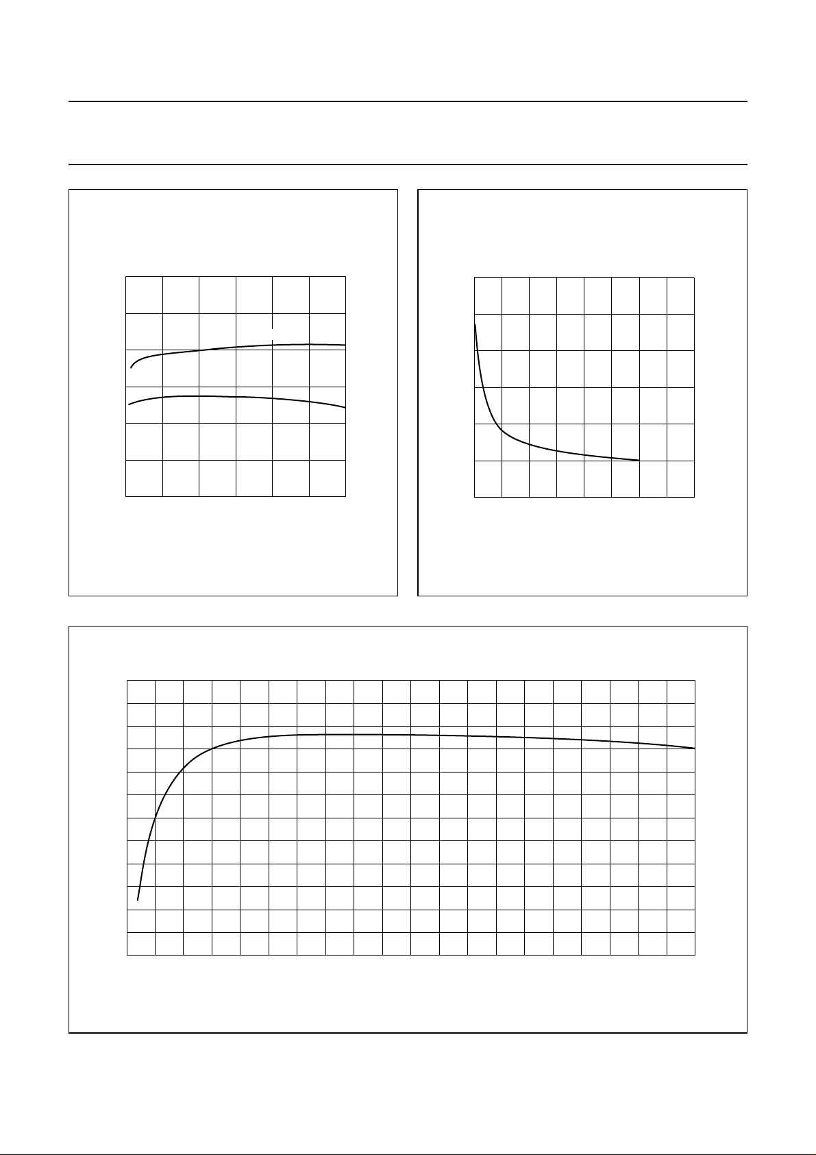
75
handbook, halfpage
h
FE
50
25
0
0 10 20 30
VCE = 28 V
5 V
IC (A)
Fig.5 Typical values; Tj=25°C.
MGP524
1500
handbook, halfpage
C
c
(pF)
1000
500
0
0
Fig.6 IE=Ie= 0; f = 1 MHz; Tj= 25 °C.
typ
20 40
VCB (V)
MGP525
400
handbook, full pagewidth
f
T
(MHz)
200
0
05 15
Fig.7 VCB= 28 V; f = 100 MHz; Tj=25°C.
August 1986 5
MGP526
typ
10
−IE (A)
20
Page 6

Philips Semiconductors Product specification
HF/VHF power transistor BLW77
APPLICATION INFORMATION
R.F. performance in s.s.b. class-AB operation (linear power amplifier)
V
= 28 V; Th= 25 °C; f1= 28,000 MHz; f2= 28,001 MHz
CE
OUTPUT POWER G
15 to 130 (P.E.P.) > 12 > 37,5 < 6,2 <−30 <−30 0,1
handbook, full pagewidth
50 Ω
p
ηdt(%) IC(A) d
3
d
5
I
C(ZS)
W dB at 130 W P.E.P. dB dB A
C1
C13
C2
C3
BD443
L1
R3
C5
R1 R4
R6
C7
BD228
C6
L5
T.U.T.
C8
+V
CC
L3
C9
C10
L4
C11
R7
L2
C14
C12
50 Ω
C15
C4 R2 R5
MGP527
Fig.8 Test circuit; s.s.b. class-AB.
August 1986 6
Page 7

Philips Semiconductors Product specification
HF/VHF power transistor BLW77
List of components:
C1 = 27 pF ceramic capacitor (500 V)
C2 = 100 pF air dielectric trimmer (single insulated rotor type)
C3 = 180 pF polystyrene capacitor
C4 = C6 = C9 = 100 nF polyester capacitor
C5 = 100 pF air dielectric trimmer (single non-insulated rotor type)
C7 = C8 = 3,9 nF ceramic capacitor
C10 = 2,2 µF moulded metallized polyester capacitor
C11 = 2 × 180 pF polysterene capacitors in parallel
C12 = 3 × 56 pF and 33 pF ceramic capacitors in parallel (500 V)
C13 = 4 × 56 pF and 68 pF ceramic capacitors in parallel (500 V)
C14 = 360 pF air dielectric trimmer (single insulated rotor type)
C15 = 360 pF air dielectric trimmer (single non-insulated rotor type)
L1 = 88 nH; 3 turns Cu wire (1,0 mm); int. dia. 9,0 mm; length 6,1 mm; leads 2 × 7 mm
L2 = L4 = Ferroxcube wide-band h.f. choke, grade 3B (cat. no. 4312 020 36640)
L3 = L5 = 80 nH; 2,5 turns closely wound enamelled Cu wire (1,6 mm); int. dia. 10,0 mm; leads 2 × 7mm
R1 = 470 Ω wirewound resistor (5,5 W)
R2 = 4,7 Ω wirewound potentiometer (3 W)
R3 = 0,55 Ω; parallel connection of 4 × 2,2 Ω carbon resistors (± 5%; 0,5 W each)
R4 = 45 Ω; parallel connection of 4 × 180 Ω wirewound resistors (5,5 W each)
R5 = 56 Ω (± 5%) carbon resistor (0,5 W)
R6 = 27 Ω (± 5%) carbon resistor (0,5 W)
R7 = 4,7 Ω (± 5%) carbon resistor (0,5 W)
August 1986 7
Page 8

Philips Semiconductors Product specification
HF/VHF power transistor BLW77
−20
handbook, halfpage
d3, d
5
(dB)
d
3
−40
−60
0
VCE= 28 V; I
= 28,001 MHz; Th= 25 °C; typical values.
f
2
d
5
= 100 mA; f1= 28,000 MHz;
C(ZS)
10050
MGP528
P.E.P. (W)
150
Fig.9 Intermodulation distortion as a function of
output power.
(1.)
1. Stated intermodulation distortion figures are referred
to the according level of either of the equal amplified
tones. Relative to the according peak envelope
powers these figures should be increased by 6 dB.
η
dt
G
p
P.E.P. (W)
MGP529
60
handbook, halfpage
η
dt
(%)
40
20
0
0 50 100 150
VCE= 28 V; I
= 28,001 MHz; Th= 25 °C; typical values.
f
2
= 100 mA; f1= 28,000 MHz;
C(ZS)
Fig.10 Double-tone efficiency and power gain as a
function of output power.
30
(dB)
20
10
0
G
p
August 1986 8
Page 9

Philips Semiconductors Product specification
HF/VHF power transistor BLW77
40
handbook, halfpage
G
p
(dB)
30
20
10
0
11010
VCE= 28 V; I
= 25 °C; ZL= 2,5 Ω.
T
h
= 100 mA; PL= 130 W;
C(ZS)
f (MHz)
Fig.11 Power gain as a function of frequency.
MGP530
2
5
handbook, halfpage
r
i
(Ω)
2.5
0
11010
VCE= 28 V; I
= 25 °C; ZL= 2,5 Ω.
T
h
= 100 mA; PL= 130 W;
C(ZS)
x
r
MGP531
i
i
f (MHz)
Fig.12 Input impedance (series components) as a
function of frequency.
1
x
i
(Ω)
0
−1
−2
−3
2
Figs 11 and 12 are typical curves and hold for an
unneutralized amplifier in s.s.b. class-AB operation.
August 1986 9
Page 10

Philips Semiconductors Product specification
HF/VHF power transistor BLW77
30
handbook, halfpage
G
p
(dB)
20
10
0
11010
VCE= 28 V; I
= 2,5Ω; neutralizing capacitor: 150 pF.
Z
L
= 100 mA; PL= 130 W; Th=25°C;
C(ZS)
f (MHz)
Fig.13 Power gain as a function of frequency.
MGP533
2
7.5
handbook, halfpage
r
i
(Ω)
5
2.5
0
11010
VCE= 28 V; I
= 2,5 Ω; neutralizing capacitor: 150 pF.
Z
L
= 100 mA; PL= 130 W; Th=25°C;
C(ZS)
x
r
MGP534
i
i
f (MHz)
Fig.14 Input impedance (series components) as a
function of frequency.
0
x
i
(Ω)
−1
−2
−3
2
13 and 14 are typical curves and hold for a push-pull
amplifier with cross-neutralization in s.s.b class-AB
operation.
August 1986 10
Page 11

Philips Semiconductors Product specification
HF/VHF power transistor BLW77
VSWR
MGP532
Th =
50 °C
70 °C
90 °C
250
handbook, halfpage
P
Lnom
(W P.E.P.)
(VSWR = 1)
200
150
100
11010
The graph shows the permissible output power under nominal
conditions (VSWR = 1) as a function of the expected VSWR during
short-time mismatch conditions with heatsink temperatures as
parameter.
Fig.15 R.F. SOAR; s.s.b. class-AB operation;
f1= 28,000 MHz; f2= 28,001 MHz;
VCE= 28 V; R
th mb-h
= 0,2 K/W.
2
August 1986 11
Page 12

Philips Semiconductors Product specification
HF/VHF power transistor BLW77
R.F. performance in c.w. operation (unneutralized common-emitter class-B circuit); Th=25°C
f (MHz) V
(V) PL(W) PS(W) Gp(dB) IC(A) η (%) zi(Ω) YL(mS)
CE
87,5 28 130 typ. 23,2 typ. 7,5 typ. 6,2 typ. 75 0,62 + j0,73 273 − j42
handbook, full pagewidth
50 Ω
C1
C2
L1
C3 C4
L5
L2
L3
T.U.T.
L4
C5
R1
+V
CC
L8
C7ab
L6
C6
R2
L7
C8
C9
50 Ω
C10
MGP535
Fig.16 Test circuit; c.w. class-B.
List of components:
C1 = 4 to 40 pF film dielectric trimmer (cat. no. 2222 809 07008)
C2 = C9 = C10 = 7 to 100 pF film dielectric trimmer (cat. no. 2222 809 07015)
C3 = C8 = 22 pF ceramic capacitor (500 V)
C4 = 4 × 82 pF ceramic capacitors in parallel (500 V)
C5 = 390 pF polystyrene capacitor
C6 = 220 nF polyester capacitor
C7a = 2 × 10 pF ceramic capacitors in parallel (500 V)
C7b = 2 × 8,2 pF ceramic capacitors in parallel (500 V)
L1 = 25 nH; 2 turns Cu wire (1,6 mm); int. dia. 5,0 mm; length 4,6 mm; leads 2 × 5 mm
L2 = L5 = 2,4 nH; strip (12 mm × 6 mm); tap for L4 and L6 at 5 mm from transistor
L3 = L7 = Ferroxcube wide-band h.f. choke, grade 3B (cat. no. 4312 020 36640)
L4 = 100 nH; 7 turns closely wound enamelled Cu wire (0,5 mm); int. dia. 3 mm; leads 2 × 5 mm
L6 = 46 nH; 2 turns Cu wire (2,0 mm); int. dia. 9,0 mm; length 6,0 mm; leads 2 × 5 mm
L8 = 44 nH; 2 turns Cu wire (2,0 mm); int. dia. 9,0 mm; length 6,7 mm; leads 2 × 5 mm
L2 and L5 are strips on a double Cu-clad printed-circuit board with epoxy fibre-glass dielectric.
R1 = 10 Ω (± 10%) carbon resistor
R2 = 10 Ω (± 10%) carbon resistor
Component layout and printed-circuit board for 87,5 MHz test circuit are shown in Fig.17.
August 1986 12
Page 13

Philips Semiconductors Product specification
HF/VHF power transistor BLW77
116
handbook, full pagewidth
65
L7
+V
CC
C8
C9
C10
MGP536
C5
L8
R2
C6
C7a
C7b
C1
C2
C3
L3
R1
L4
L1
L2 L5
C4
rivet
L6
strip
Fig.17 Component layout and printed-circuit board for 87,5 MHz test circuit.
The circuit and the components are situated on one side of the epoxy fibre-glass board, the other side being fully
metallized to serve as earth. Earth connections are made by means of hollow rivets, whilst under the emitter leads Cu
straps are used for a direct contact between upper and lower sheets.
August 1986 13
Page 14

Philips Semiconductors Product specification
HF/VHF power transistor BLW77
250
handbook, halfpage
P
L
(W)
200
150
100
50
0
0255075
typ
Fig.18 VCE= 28 V; f = 87,5 MHz; Th=25°C.
175
handbook, halfpage
PS (W)
MGP537
MGP539
10
handbook, halfpage
G
p
(dB)
5
0
0 100 200 300
η
G
p
PL (W)
Fig.19 VCE= 28 V; f = 87,5 MHz; Th=25°C;
typical values.
MGP538
100
η
(%)
50
0
P
Lnom
(W)
(VSWR = 1)
125
Th =
50 °C
70 °C
75
11010
The graph shows the permissible output power under
nominal conditions (VSWR = 1) as a function of the
expected VSWR during short-time mismatch
conditions with heatsink temperatures as parameter.
VSWR
90 °C
2
Fig.20 R.F. SOAR; c.w. class-B operation;
f = 87,5 MHz; VCE= 28 V;
R
th mb-h
= 0,2 K/W.
August 1986 14
Page 15

Philips Semiconductors Product specification
HF/VHF power transistor BLW77
handbook, halfpage
2
ri, x
i
(Ω)
0
−2
0 100 200
r
i
x
i
f (MHz)
MGP540
Fig.21 VCE= 28 V; PL=130 W; Th=25°C; typical
values.
handbook, halfpage
5
R
L
(Ω)
0
−5
−10
0 100 200
R
L
C
L
f (MHz)
MGP541
Fig.22 VCE= 28 V; PL=130 W; Th=25°C; typical
values.
0.5
C
(nF)
0
−0.5
−1
L
20
handbook, halfpage
G
p
(dB)
10
0
0 50 100 150
typ
MGP542
f (MHz)
Fig.23 VCE= 28 V; PL=130 W; Th=25°C.
August 1986 15
Page 16

Philips Semiconductors Product specification
HF/VHF power transistor BLW77
PACKAGE OUTLINE
Flanged ceramic package; 2 mounting holes; 4 leads SOT121B
D
A
F
H
43
α
12
H
q
U
1
L
C
B
b
p
w
M
C
2
A
U
U
2
w
M
AB
1
D
3
1
c
Q
0 5 10 mm
scale
DIMENSIONS (millimetre dimensions are derived from the original inch dimensions)
5.82
5.56
c
Db
12.83
12.86
0.16
0.10
0.006
0.004
IEC JEDEC EIAJ
12.59
0.506
0.496
12.57
0.505
0.495
F
D
1
2.67
28.45
2.41
25.52
1.120
0.105
0.095
0.312
1.005
0.249
REFERENCES
7.93
6.32
0.130
0.120
UNIT
inches
A
7.27
mm
6.17
0.229
0.286
0.219
0.243
OUTLINE
VERSION
SOT121B 97-06-28
pH
3.30
3.05
Q
4.45
3.91
0.175
0.154
q
18.42
0.725
U
1
24.90
24.63
0.98
0.97
U
2
6.48
6.22
0.255
0.245
w1w
U
3
12.32
0.51
12.06
0.485
0.02
0.475
EUROPEAN
PROJECTION
August 1986 16
2
1.02
0.04
ISSUE DATE
αL
45°
Page 17

Philips Semiconductors Product specification
HF/VHF power transistor BLW77
DEFINITIONS
Data Sheet Status
Objective specification This data sheet contains target or goal specifications for product development.
Preliminary specification This data sheet contains preliminary data; supplementary data may be published later.
Product specification This data sheet contains final product specifications.
Limiting values
Limiting values given are in accordance with the Absolute Maximum Rating System (IEC 134). Stress above one or
more of the limiting values may cause permanent damage to the device. These are stress ratings only and operation
of the device at these or at any other conditions above those given in the Characteristics sections of the specification
is not implied. Exposure to limiting values for extended periods may affect device reliability.
Application information
Where application information is given, it is advisory and does not form part of the specification.
LIFE SUPPORT APPLICATIONS
These products are not designed for use in life support appliances, devices, or systems where malfunction of these
products can reasonably be expected to result in personal injury. Philips customers using or selling these products for
use in such applications do so at their own risk and agree to fully indemnify Philips for any damages resulting from such
improper use or sale.
August 1986 17
 Loading...