

Page 1

DISCRETE SEMICONDUCTORS
DATA SH EET
BLW60C
VHF power transistor
Product specification
March 1993
Page 2
Philips Semiconductors Product specification
VHF power transistor BLW60C
DESCRIPTION
N-P-N silicon planar epitaxial
transistor intended for use in class-A,
B and C operated mobile, industrial
and military transmitters with a
Matched h
request.
It has a 3/8" capstan envelope with a
ceramic cap. All leads are isolated
from the stud.
groups are available on
FE
nominal supply voltage of 12,5 V. The
transistor is resistance stabilized and
is guaranteed to withstand severe
load mismatch conditions with a
supply over-voltage to 16,5 V.
QUICK REFERENCE DATA
R.F. performance up to T
MODE OF OPERATION
=25°C
h
V
CC
VfMHz
P
W
L
G
L
dB
%
η
z
i
Ω
Z
L
Ω
d
dB
3
c.w. (class-B) 12,5 175 45 > 5,0 > 75 1,2 + j1,4 2,6 − j1,2 −
s.s.b. (class-AB) 12,5 1,6-28 3-30 (P.E.P.) typ. 19,5 typ. 35 −−typ. −33
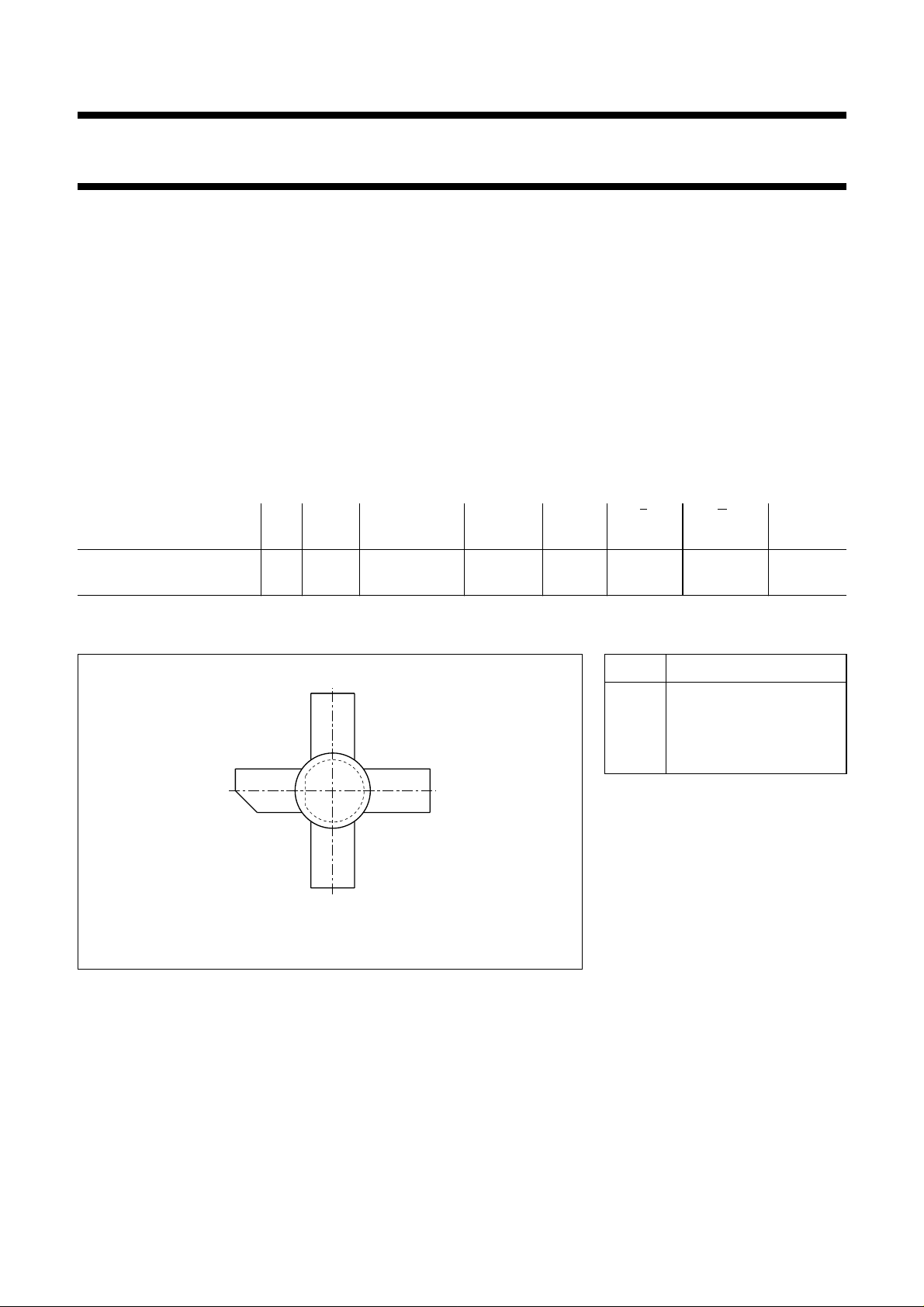
PIN CONFIGURATION
PINNING - SOT120A.
PIN DESCRIPTION
handbook, halfpage
4
1 collector
2 emitter
3 base
31
4 emitter
2
MSB056
Fig.1 Simplified outline. SOT120A.
PRODUCT SAFETY This device incorporates beryllium oxide, the dust of which is toxic. The device is entirely
safe provided that the BeO disc is not damaged.
March 1993 2
Page 3

Philips Semiconductors Product specification
VHF power transistor BLW60C
RATINGS
Limiting values in accordance with the Absolute Maximum System (IEC 134)
Collector-emitter voltage (V
peak value V
Collector-emitter voltage (open base) V
Emitter-base voltage (open collector) V
Collector current (average) I
Collector current (peak value); f > 1 MHz I
R.F. power dissipation (f > 1 MHz); T
Storage temperature T
Operating junction temperature T
BE
=0)
CESM
CEO
EBO
C(AV)
CM
= 25 °CP
mb
rf
stg
j
max. 36 V
max. 16 V
max. 4 V
max. 9 A
max. 22 A
max. 100 W
−65 to+ 150 °C
max. 200 °C
CE
(V)
MGP479
2
150
handbook, halfpage
P
rf
(W)
100
50
0
0
I Continuous d.c. operation
II Continuous r.f. operation
III Short-time operation during mismatch
Fig.3 R.F. power dissipation; VCE≤ 16,5 V; f > MHz.
2
10
handbook, halfpage
I
C
(A)
10
1
11010
Th = 70 °C
Fig.2 D.C. SOAR.
Tmb = 25 °C
V
THERMAL RESISTANCE
(dissipation = 40 W; T
=88°C, i.e. Th=70°C)
mb
From junction to mounting base (d.c. dissipation) R
From junction to mounting base (r.f. dissipation) R
From mounting base to heatsink R
ΙΙΙ
ΙΙ
Ι
50
th j-mb(dc)
th j-mb(rf)
th mb-h
derate by 0.52 W/K
0.38 W/K
Th (°C)
= 2,8 K/W
= 2,05 K/W
= 0,45 K/W
MGP480
100
March 1993 3
Page 4

Philips Semiconductors Product specification
VHF power transistor BLW60C
CHARACTERISTICS
T
=25°C
j
Breakdown voltage
Collector-emitter voltage
=0;IC=50mA V
V
BE
(BR)CES
Collector-emitter voltage
open base; I
= 100 mA V
C
(BR)CEO
Emitter-base voltage
open collector; IE=25mA V
(BR)EBO
Collector cut-off current
=0;VCE=15V I
V
BE
CES
Transient energy
L = 25 mH; f = 50 Hz
open base E > 8ms
−VBE= 1,5 V; RBE=33Ω E > 8ms
D.C. current gain
IC= 4 A; VCE=5V h
D.C. current gain ratio of matched devices
IC= 4 A; VCE=5V h
Collector-emitter saturation voltage
IC= 12,5 A; IB= 2,5 A V
Transition frequency at f = 100 MHz
IC= 4 A; VCE= 12,5 V f
I
= 12,5 A; VCE= 12,5 V f
C
(1)
FE
(1)
FE1/hFE2
(1)
CEsat
(1)
T
T
Collector capacitance at f = 1 MHz
= 0; VCB=15V C
I
E=Ie
c
> 36 V
> 16 V
> 4V
< 25 mA
typ 50
10 to 80
< 1,2
typ 1,5 V
typ 650 MHz
typ 600 MHz
typ 120 pF
< 160 pF
Feedback capacitance at f = 1 MHz
I
= 200 mA; VCE=15V C
C
Collector-stud capacitance
Note
1. Measured under pulse conditions: t
≤ 200 µs; δ≤0,02.
p
March 1993 4
re
C
cs
typ 80 pF
typ 2 pF
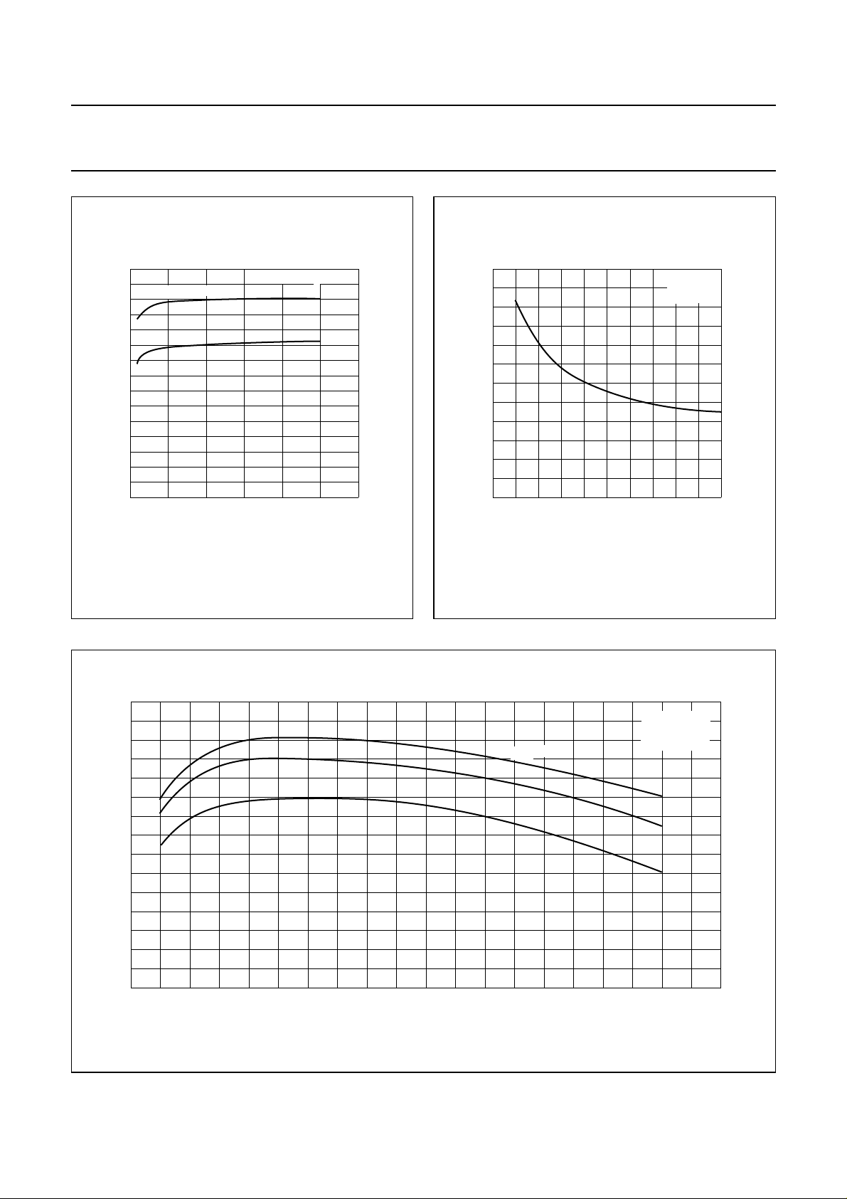
Page 5
Philips Semiconductors Product specification
VHF power transistor BLW60C
75
handbook, halfpage
h
FE
50
25
0
0 5 10 15
typical values Tj = 25 °C
VCE = 12.5 V
5 V
MGP481
IC (A)
Fig.4 DC current gain as a function of collector
current.
300
handbook, halfpage
C
c
(pF)
200
100
0
01020
typ
IE = Ie = 0
f = 1 MHz
VCB (V)
Fig.5 Collector capacitance as a function of
collector-base voltage.
MGP482
750
handbook, full pagewidth
f
T
(MHz)
500
250
0
0510
VCE = 12.5 V
10 V
5 V
15
Fig.6 Transition frequency as a function of collector current.
typical values
f = 100 MHz
Tj = 25 °C
IC (A)
MGP483
20
March 1993 5
Page 6

Philips Semiconductors Product specification
VHF power transistor BLW60C
APPLICATION INFORMATION
R.F. performance in c.w. operation (unneutralized common-emitter class-B circuit); T
=25°C
h
f (MHz) V
(V) PL (W) PS (W) Gp(dB) IC(A) η (%) zi(Ω) ZL(Ω)
CC
175 12,5 45 < 14,2 > 5,0 < 4,8 > 75 1,2 + j1,4 2,6 − j1,2
175 13,5 45 − typ. 6,0 − typ. 75 −−
Test circuit for 175 MHz
handbook, full pagewidth
C6a
R2
MGP484
C6b
C7
50 Ω
C8
50 Ω
C1
C2
+V
L7
L6
C5
L8
CC
C3a
L1
L2
R1
T.U.T.
L4
C3b
L3
L5
C4
Fig.7 Class-B test circuit at f = 175 MHz.
List of components:
C1 = 2,5 to 20 pF film dielectric trimmer (cat. no. 2222 809 07004)
C2 = C8 = 4 to 40 pF film dielectric trimmer (cat. no. 2222 809 07008)
C3a = C3b = 47 pF ceramic capacitor (500 V)
C4 = 120 pF ceramic capacitor
C5 = 100 nF polyester capacitor
C6a = C6b = 8,2 pF ceramic capacitor (500 V)
C7 = 5 to 60 pF film dielectric trimmer (cat. no. 2222 809 07011)
L1 = 1 turn Cu wire (1,6 mm); int. dia. 9,0 mm; leads 2 × 5mm
L2 = 100 nH; 7 turns closely wound enamelled Cu wire (0,5 mm); int. dia. 3 mm; leads 2 × 5 mm
L3 = L8 = Ferroxcube wide-band h.f. choke, grade 3B (cat. no. 4312 020 36640)
L4 = L5 = strip (12 mm × 6 mm); taps for C3a and C3b at 5 mm from transistor
L6 = 2 turns enamelled Cu wire (1,6 mm); int. dia. 5,0 mm; length 6,0 mm; leads 2 × 5 mm
L7 = 2 turns enamelled Cu wire (1,6 mm); int. dia. 4,5 mm; length 6,0 mm; leads 2 × 5 mm
L4 and L5 are strips on a double Cu-clad printed-circuit board with epoxy fibre-glass dielectric, thickness 1/16".
R1 = 10 Ω (±10%) carbon resistor
R2 = 4,7 Ω (±5%) carbon resistor
Component layout and printed-circuit board for 175 MHz test circuit: Fig.8.
March 1993 6
Page 7

Philips Semiconductors Product specification
VHF power transistor BLW60C
150
handbook, full pagewidth
72
1888MJK
C1 C2
L8L3
R1
C3a
L2
L1
L4 L5
C3b
C4
C5
L6
C6a
L7
C6b
C7
R2
+V
CC
C8
1888MJK
rivet
MGP485
The circuit and the components are situated on one side of the epoxy fibre-glass board, the other side being fully metallized to serve
as earth. Earth connections are made by means of hollow rivets, whilst under the emitter leads Cu straps are used for a direct contact
between upper and lower sheets.
Fig.8 Component layout and printed-circuit board for 175 MHz class-B test circuit.
March 1993 7
Page 8

Philips Semiconductors Product specification
VHF power transistor BLW60C
100
handbook, halfpage
handbook, halfpage
P
Lnom
VSWR = 1
typical values
f = 175 MHz
P
L
(W)
75
50
25
0
010 30
50
(W)
40
30
1 1.1 1.2 1.3
VCC = 12.5 V
VCC = 13.5 V
Th = 25 °C
Th = 70 °C
Fig.9
20
VSWR =
5
10
20
50
PS (W)
P
P
Snom
V
CC
V
CCnom
MGP486
MGP488
S
MGP487
10
handbook, halfpage
G
p
(dB)
5
0
10 30 50
typical values
f = 175 MHz
Th = 25 °C
η
G
p
VCC = 12.5 V
VCC = 13.5 V
PL (W)
100
η
(%)
50
0
Fig.10
Conditions for R.F. SOAR
f = 175 MHz
Th=70°C
R
V
PS=P
= 0,45 K/W
th mb-h
= 12,5 V or 13,5 V
CCnom
Snom
at V
and VSWR = 1
CCnom
measured in circuit of Fig.7.
The transistor has been developed for use with
unstabilized supply voltages. As the output power and
drive power increase with the supply voltage, the nominal
output power must be derated in accordance with the
graph for safe operation at supply voltages other than the
nominal. The graph shows the permissible output power
under nominal conditions (VSWR = 1), as a function of the
expected supply over-voltage ratio with VSWR as
parameter.
The graph applies to the situation in which the drive
(PS/P
) increases linearly with supply over-voltage
Snom
ratio.
Fig.11
March 1993 8
Page 9

Philips Semiconductors Product specification
VHF power transistor BLW60C
handbook, halfpage
2
ri, x
i
(Ω)
0
−2
−4
0 100 200
Typical values; VCE= 12,5 V; PL=45W;
class-B operation; T
h
=25°C.
r
i
x
i
f (MHz)
Fig.12 Input impedance (series components).
MGP489
4
handbook, halfpage
RL, X
L
(Ω)
R
2
0
−2
0 100 200
Typical values; VCE= 12,5 V; PL=45W;
class-B operation; T
=25°C.
h
L
X
L
f (MHz)
Fig.13 Load impedance (series components).
MGP490
20
handbook, halfpage
G
p
(dB)
10
0
0 100 200
Typical values; VCE= 12,5 V; PL=45W;
class-B operation; T
=25°C.
h
f (MHz)
MGP491
Fig.14
March 1993 9
Page 10

Philips Semiconductors Product specification
VHF power transistor BLW60C
R.F. performance in s.s.b. class-AB operation
VCE= 12,5 V; Thup to 25 °C; R
f1= 28,000 MHz; f2= 28,001 MHz
th mb-h
≤ 0,45 K/W
OUTPUT POWER
W
G
dB
p
η
dt
%
dB
d
3
(1)
dB
d
5
(1)
I
C(ZS)
mA
3 to 30 (P.E.P.) typ 19,5 typ 35 typ −33 typ −36 25
Note
1. Stated intermodulation distortion figures are referred to the according level of either of the equal amplified tones.
Relative to the according peak envelope powers these figures should be increased by 6 dB.
handbook, full pagewidth
RS =
50 Ω
R4
R3
TR1
C1
C2
C16
C15
C3
R5
TR2
R6
L1
C4
+VB = 12.5 V
bias
T.U.T.
R1L2
C5
C9
C7
C8
R2
L4
C6
L3 C12
C10
C11
C13 C14
L5
RL =
50 Ω
+VB = 12.5 V
MGP492
Fig.15 S.S.B. class-AB test circuit.
March 1993 10
Page 11

Philips Semiconductors Product specification
VHF power transistor BLW60C
List of components:
TR1 = TR2 = BD137
C1 = 100 pF air dielectric trimmer (single insulated rotor type)
C2 = 27 pF ceramic capacitor
C3 = 180 pF ceramic capacitor
C4 = 100 pF air dielectric trimmer (single non-insulated rotor type)
C5 = C7 = 3,9 nF polyester capacitor
C6 = 2 × 270 pF polystyrene capacitors in parallel
C8 = C15 = C16 = 100 nF polyester capacitor
C9 = 2,2 µF moulded metallized polyester capacitor
C10 = 2 × 385 pF film dielectric trimmer
C11 = 68 pF ceramic capacitor
C12 = 2 x 82 pF ceramic capacitors in parallel
C13 = 47 pF ceramic capacitor
C14 = 385 pF film dielectric trimmer
L1 = 88 nH; 3 turns Cu wire (1,0 mm); int. dia. 9 mm; length 6,1 mm; leads 2 × 5 mm
L2 = L5 = Ferroxcube choke coil (cat. no. 4312 020 36640)
L3 = 68 nH; 3 turns enamelled Cu wire (1,6 mm); int. dia. 8 mm; length 8,3 mm; leads 2 × 5 mm
L4 = 96 nH; 3 turns enamelled Cu wire (1,6 mm); int. dia. 10 mm; length 7,6 mm; leads 2 × 5 mm
R1 = 27 Ω (± 5%) carbon resistor
R2 = 4,7 Ω (±5%) carbon resistor
R3 = 1,5 kΩ (±5%) carbon resistor
R4 = 10 Ω wirewound potentiometer (3 W)
R5 = 47 Ω wirewound resistor (5,5 W)
R6 = 150 Ω (±5%) carbon resistor
Measuring conditions for Figs 16 and 17:
V
= 12,5 V
CC
f
= 28,000 MHz
1
f
= 28,001 MHz
2
=25°C
T
h
R
I
C(ZS)
th mb-h
=25mA
≤ 0,45 ° K/W
typical values
March 1993 11
Measuring conditions for Figs 18 and 19:
V
= 13,5 V
CC
f
= 28,000 MHz
1
f
= 28,001 MHz
2
=25°C
T
h
R
I
C(ZS)
th mb-h
≤ 0,45 ° K/W
=25mA
typical values
Page 12

Philips Semiconductors Product specification
VHF power transistor BLW60C
−20
handbook, halfpage
d3, d
5
(dB)
−40
−60
02040
intermodulation distortion versus
output power *
Fig.16
d
d
P.E.P. (W)
3
5
MGP493
40
handbook, halfpage
double-tone efficiency versus
output power
η
dt
(%)
20
0
02040
MGP494
typ
P.E.P. (W)
Fig.17
−20
handbook, halfpage
d3, d
intermodulation distortion versus
output power *
5
(dB)
−40
−60
02040
Fig.18
P.E.P. (W)
MGP495
d
3
d
5
40
handbook, halfpage
double-tone efficiency versus
output power
η
dt
(%)
20
0
02040
typ
P.E.P. (W)
Fig.19
MGP496
* Stated intermodulation distortion figures are referred to the according level of either of the equal amplified tones.
Relative to the according peak envelope powers these figures should be increased by 6 dB.
March 1993 12
Page 13

Philips Semiconductors Product specification
VHF power transistor BLW60C
f (MHz)
MGP497
2
10
handbook, halfpage
r
i
(Ω)
7.5
5
2.5
0
11010
input impedance (series components)
versus frequency
30
handbook, halfpage
G
p
(dB)
20
10
11010
Fig.20
S.S.B. class-AB operation
Conditions for Figs 20 and 21:
V
= 12,5 V VCC= 13,5 V
CC
= 30 W (P.E.P.) PL= 35 W (P.E.P.)
P
L
T
=25°CT
h
R
I
C(ZS)
Z
≤ 0,45 K/W R
th mb-h
=25mA I
= 1,9 Ω ZL= 1,9 Ω
L
=25°C
h
≤ 0,45 K/W
th mb-h
=25mA
C(ZS)
The typical curves (both conditions) hold for an unneutralized amplifier.
Fig.21
x
i
r
i
f (MHz)
MGP498
5
x
i
(Ω)
2.5
0
−2.5
−5
2
March 1993 13
Page 14

Philips Semiconductors Product specification
VHF power transistor BLW60C
PACKAGE OUTLINE
Studded ceramic package; 4 leads SOT120A
D
A
Q
c
D
N
1
N
N
3
L
H
1
1
D
2
H
b
4
A
w
A
M
1
X
3
2
M
M
1
detail X
W
0 5 10 mm
scale
DIMENSIONS (millimetre dimensions are derived from the original inch dimensions)
5.90
5.48
c
Db
9.73
0.18
9.47
0.14
0.383
0.007
0.373
0.004
IEC JEDEC EIAJ
D
1
8.39
8.12
0.330
0.320
D
2
9.66
9.39
0.380
0.370
27.44
9.00
25.78
8.00
1.080
0.354
1.015
0.315
REFERENCES
L
MH
3.41
2.92
0.134
0.065
0.115
0.055
UNIT
mm
inches
A W
5.97
4.74
0.232
0.283
0.216
0.248
OUTLINE
VERSION
SOT120A
March 1993 14
M
1.66
1.39
8-32
UNC
w
0.38
0.015
1
ISSUE DATE
97-06-28
N
N
1
12.83
11.17
0.505
0.440
1
1.60
0.00
0.063
0.000
N
3.31
2.54
0.130
0.100
3
Q
4.35
3.98
0.171
0.157
EUROPEAN
PROJECTION
Page 15

Philips Semiconductors Product specification
VHF power transistor BLW60C
DEFINITIONS
Data Sheet Status
Objective specification This data sheet contains target or goal specifications for product development.
Preliminary specification This data sheet contains preliminary data; supplementary data may be published later.
Product specification This data sheet contains final product specifications.
Limiting values
Limiting values given are in accordance with the Absolute Maximum Rating System (IEC 134). Stress above one or
more of the limiting values may cause permanent damage to the device. These are stress ratings only and operation
of the device at these or at any other conditions above those given in the Characteristics sections of the specification
is not implied. Exposure to limiting values for extended periods may affect device reliability.
Application information
Where application information is given, it is advisory and does not form part of the specification.
LIFE SUPPORT APPLICATIONS
These products are not designed for use in life support appliances, devices, or systems where malfunction of these
products can reasonably be expected to result in personal injury. Philips customers using or selling these products for
use in such applications do so at their own risk and agree to fully indemnify Philips for any damages resulting from such
improper use or sale.
March 1993 15
 Loading...