

Page 1

DISCRETE SEMICONDUCTORS
DATA SH EET
BLW33
UHF linear power transistor
Product specification
August 1986
Page 2

Philips Semiconductors Product specification
UHF linear power transistor BLW33
DESCRIPTION
N-P-N silicon planar epitaxial
transistor primarily intended for use in
linear u.h.f. amplifiers for television
transmitters and transposers. The
excellent d.c. dissipation
properties for class-A operation are
area. The combination of optimum
thermal design and the application of
gold sandwich metallization
realizes excellent reliability
properties.
1
The transistor has a
⁄4" capstan
envelope with ceramic cap.
obtained by means of diffused emitter
ballasting resistors and a multi-base
structure, providing an optimum
temperature profile on the crystal
QUICK REFERENCE DATA
R.F. performance
MODE OF OPERATION f
vision
MHz
V
CE
V
I
C
mA
T
°C
h
(1)
d
im
P
dB
o sync
W
(1)
G
dB
p
class-A; linear amplifier 860 25 300 70 −60 > 1,0 > 10,0
860 25 300 25 −60 typ. 1,15 typ. 10,5
Note
1. Three-tone test method (vision carrier −8 dB, sound carrier −7 dB, sideband signal−16 dB), zero dB corresponds to
peak sync level.
PIN CONFIGURATION
PINNING - SOT122A.
PIN DESCRIPTION
1 collector
2 emitter
Top view
4
31
2
MBK187
3 base
4 emitter
handbook, halfpage
Fig.1 Simplified outline. SOT122A.
PRODUCT SAFETY This device incorporates beryllium oxide, the dust of which is toxic. The device is entirely
safe provided that the BeO disc is not damaged.
August 1986 2
Page 3
Philips Semiconductors Product specification
UHF linear power transistor BLW33
RATINGS
Limiting values in accordance with the Absolute Maximum System (IEC 134)
Collector-emitter voltage
(peak value); V
open base V
Emitter-base voltage (open collector) V
Collector current
d.c. or average I
(peak value); f > 1 MHz I
Total power dissipation up to T
Storage temperature T
Operating junction temperature T
=0 V
BE
=25°CP
mb
CESM
CEO
EBO
C
CM
tot
stg
j
max. 50 V
max. 30 V
max. 4 V
max. 1,25 A
max. 1,9 A
max. 19,3 W
−65 to +150 °C
max. 200 °C
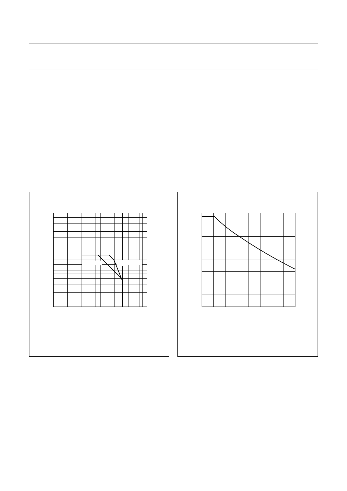
10
handbook, halfpage
I
C
(A)
(1)
1
−1
10
11010
(1) Second breakdown limit (independent of temperature).
Th = 70 °C
Tmb = 25 °C
VCE (V)
Fig.2 D.C. SOAR.
THERMAL RESISTANCE (see Fig.4)
MGP442
2
20
handbook, halfpage
P
tot
(W)
15
10
5
0
0 50 100
Th (°C)
Fig.3 Power derating curve vs. temperature.
MGP443
From junction to mounting base
(dissipation = 7,5 W; Tmb= 74,5 °C; i.e. Th=70°C) R
From mounting base to heatsink R
August 1986 3
th j-mb
th mb-h
= 10,1 K/W
= 0,6 K/W
Page 4

Philips Semiconductors Product specification
UHF linear power transistor BLW33
15
handbook, full pagewidth
R
th j-h
(K/W)
10
5
0 5 10 15 20
100 °C
125 °C
Th = 125 °C
150 °C
100 °C
75 °C
50 °C
25 °C
Tj = 200 °C
175 °C
0 °C
P
MGP444
(W)
tot
Fig.4 Maximum thermal resistance from junction to heatsink as a function of power dissipation, with heatsink
and junction temperature as parameters. (R
th mb-h
= 0,6 K/W.)
25
Example
Nominal class-A operation: V
Fig.4 shows: R
Typical device: R
T
T
th j-h
j
th j-h
j
= 25 V; IC= 300 mA; Th=70°C.
CE
max. 10,7 K/W
max. 150 °C
typ. 8,25 K/W
typ. 132 °C
August 1986 4
Page 5

Philips Semiconductors Product specification
UHF linear power transistor BLW33
CHARACTERISTICS
T
=25°C unless otherwise specified
j
Collector-emitter breakdown voltage
V
= 0; IC= 4 mA V
BE
open base; I
= 30 mA V
C
(BR)CES
(BR)CEO
Emitter-base breakdown voltage
open collector; I
= 2 mA V
E
(BR)EBO
Collector cut-off current
VBE= 0; VCE= 30 V I
= 0; VCE= 30 V; Tj= 175 °CI
V
BE
CES
CES
D.C. current gain
I
= 300 mA; VCE= 25 V h
C
FE
> 50 V
> 30 V
> 4V
< 1,0 mA
< 2,5 mA
>
typ.2040
IC= 300 mA; VCE= 25 V; Tj= 175 °Ch
Collector-emitter saturation voltage
(1)
IC= 600 mA; IB= 60 mA V
Transition frequency at f = 500 MHz
(2)
−IE= 300 mA; VCB= 25 V f
−I
= 600 mA; VCB= 25 V f
E
FE
CEsat
T
T
< 120
typ. 450 mV
typ. 3,4 GHz
typ. 3,1 GHz
Collector capacitance at f = 1 MHz
I
= 0; VCB= 25 V C
E=Ie
c
typ. 6,6 pF
Feedback capacitance at f = 1 MHz
IC= 20 mA; VCE= 25 V C
Collector-stud capacitance C
re
cs
typ. 3,5 pF
typ. 1,2 pF
Notes
1. Measured under pulse conditions: t
≤ 300 µs; δ≤0,02.
p
2. Measured under pulse conditions: tp≤ 50 µs; δ≤0,01.
August 1986 5
Page 6

Philips Semiconductors Product specification
UHF linear power transistor BLW33
50
handbook, halfpage
h
FE
25
0
0 0.5 1 1.5
MGP445
VCE = 25 V
5 V
IC (A)
Fig.5 Typical values; Tj=25°C.
25
handbook, halfpage
C
c
(pF)
20
15
10
5
0
0102030
Fig.6 IE=Ie= 0; f = 1 MHz; Tj=25°C.
MGP446
typ
VCB (V)
handbook, full pagewidth
4
f
T
(GHz)
3
2
1
0
0 0.5
typ
Fig.7 VCB= 25 V; f = 500 MHz; Tj=25°C.
MGP447
1
−IE (A)
1.5
August 1986 6
Page 7

Philips Semiconductors Product specification
UHF linear power transistor BLW33
APPLICATION INFORMATION
f
(MHz) VCE(V) IC(mA) Th(°C) dim(dB)
vision
(1)
P
o sync
(W)
(1)
GP (dB)
860 25 300 70 −60 > 1,0 > 10
860 25 300 70 −60 typ. 1,07 typ. 10,5
860 25 300 25 −60 typ. 1,15 typ. 10,5
Note
1. Three-tone test method (vision carrier −8 dB, sound carrier −7 dB, sideband signal −16 dB), zero dB corresponds to
peak sync level.
handbook, full pagewidth
50 Ω
C1 C3
L1 L2 L3
C9C2C10 C11
+V
Fig.8 Test circuit at f
BB
T.U.T.
L5
C4L4
C5 C8
L6
+V
C12 C13 C14 C15
CC
= 860 MHz.
vision
C6
L8C7L7
50 Ω
MGP448
List of components:
C1 = C3 = 2 to 18 pF film dielectric trimmer (cat. no. 2222 809 05003)
C2 = C6 = C8 = 1 to 3,5 pF film dielectric trimmer (cat. no. 2222 809 05001) placed 24 mm, 8 mm
and 46 mm respectively from transistor edge
C4 = C5 = 4,3 pF multilayer ceramic chip capacitor (ATC 100A-4R3-C-PX-50)
C7 = 1,8 to 10 pF film dielectric trimmer (cat. no. 2222 809 05002)
C9 = C12 = 1 nF chip capacitor
C10 = 100 nF polyester capacitor
C11 = C13 = 470 nF polyester capacitor
C14 = 10 nF polyester capacitor
C15 = 3,3 µF/40 F solid aluminium electrolytic capacitor
L1 = stripline (5,2 mm × 4,5 mm)
L2 = stripline (13,2 mm × 4,5 mm)
L3 = stripline (15,0 mm × 4,5 mm)
L4 = micro choke 0,47 µH (cat. no. 4322 057 04770)
L5 = stripline (see Fig.9 printed-circuit board layout)
L6 = 4 turns closely wound enamelled Cu wire (1,0 mm); int. dia. 5,5 mm; leads 2 × 4 mm
L7 = stripline (37,0 mm × 4,5 mm)
L8 = stripline (13,5 mm × 4,5 mm)
August 1986 7
Page 8

Philips Semiconductors Product specification
UHF linear power transistor BLW33
L1; L2; L3; L5; L7 and L8 are striplines on a double Cu-clad printed-circuit board with PTFE fibre-glass dielectric
(εr= 2,74); thickness 1/16".
For bias circuit see Fig.10.
handbook, full pagewidth
L1
C1 C3
C11
L2
C2
C10
114.5
46
+V
CC
C14
C15
C13
L7
L8
C7
C8
+V
BB
C9
L4
C4
L3
C5
C12
L6
L5
C6
MGP449
Fig.9 Component layout and printed-circuit board for 860 MHz test circuit.
The circuit and the components are situated on one side of the PTFE fibre-glass board, the other side being fully
metallized to serve as earth. Earth connections are made by means of hollow rivets, whilst under the emitter leads Cu
straps are used for a direct contact between upper and lower sheets.
August 1986 8
Page 9

Philips Semiconductors Product specification
UHF linear power transistor BLW33
D2
R1
D1
R2
C2C1
R3
C3
R5R4
C4
R6
TR1
Fig.10 Bias circuit for class-A amplifier at
f
= 860 MHz.
vision
−50
handbook, full pagewidth
d
im
(dB)
R7
R8
R9
MGP437
+V
+V
+V
List of components:
s
C1 = 100 pF ceramic capacitor
C2 = C3 = 100 nF polyester capacitor
CC
C4 = 10 µF/25 V solid aluminium electrolytic capacitor
R1 = 150 Ω carbon resistor (0,25 W)
R2 = 100 Ω preset potentiometer (0,1 W)
R3 = 82 Ω carbon resistor (0,25 W)
BB
R4 = R5 = 2,2 kΩ carbon resistor (0,25 W)
R6 = 6 Ω; parallel connection of 2 × 12 Ω
carbon resistors (0,5 W each)
R7 = R8 = 820 Ω carbon resistor (0,25 W)
0
R9 = 33 Ω carbon resistor (0,25 W)
D1 = BZY88-C3V3
D2 = BY206
TR1 = BD136
MGP450
30
d
cm
d
im
(%)
−55
−60
−65
01 3
Fig.11 Intermodulation distortion (dim)
(1.)
and cross-modulation distortion (dcm)
Typical values; VCE= 25 V; IC= 300 mA; f
d
cm
2
(2.)
as a function of output power.
= 860 MHz; − − − Th=25°C; Th=70°C.
vision
P
o sync
(W)
20
10
0
4
Information for wideband application from 470 to 860 MHz available on request.
1. Three-tone test method (vision carrier −8 dB, sound carrier −7 dB, sideband signal −16 dB), zero dB corresponds to
peak sync level.
Intermodulation distortion of input signal ≤−75 dB.
2. Two-tone test method (vision carrier 0 dB, sound carrier −7 dB), zero dB corresponds to peak sync level.
Cross-modulation distortion (d
) is the voltage variation (%) of sound carrier when vision carrier is switched from
cm
0 dB to −20 dB.
August 1986 9
Page 10

Philips Semiconductors Product specification
UHF linear power transistor BLW33
handbook, halfpage
5
ri, x
i
(Ω)
0
−5
−10
−15
10 10
Typical values; VCE= 25 V;
= 300 mA; Th=70°C.
I
C
r
i
x
i
2
f (MHz)
Fig.12 Input impedance (series components).
MGP451
f (MHz)
MGP452
3
10
50
handbook, halfpage
RL, X
L
(Ω)
25
3
10
0
10 10
Typical values; VCE= 25 V;
= 300 mA; Th=70°C.
I
C
R
L
X
L
2
Fig.13 Load impedance (series components).
35
handbook, halfpage
G
p
(dB)
25
15
5
10 10
Typical values; VCE= 25 V;
= 300 mA; Th=70°C.
I
C
2
Fig.14
f (MHz)
MGP453
Ruggedness
The BLW33 is capable of withstanding a load mismatch
(VSWR = 50 through all phases) under the following
conditions:
f = 860 MHz; VCE= 25 V; IC= 300 mA;
Th=70°C and PL= 2 W.
3
10
August 1986 10
Page 11

Philips Semiconductors Product specification
UHF linear power transistor BLW33
PACKAGE OUTLINE
Studded ceramic package; 4 leads SOT122A
D
A
Q
N
1
N
N
3
L
H
D
1
D
2
H
b
4
ceramic
BeO
metal
A
w
X
c
A
M
1
M
M
1
detail X
W
α
3
1
2
0 5 10 mm
scale
DIMENSIONS (millimetre dimensions are derived from the original inch dimensions)
UNIT
mm
OUTLINE
VERSION
SOT122A
A
5.97
4.74
b
5.85
5.58
D
6.48
6.22
D
1
2
27.56
7.24
25.78
6.93
REFERENCES
cM
D
0.18
7.50
0.14
7.23
IEC JEDEC EIAJ
L
H
9.91
3.18
9.14
2.66
August 1986 11
N
M
1
1.66
1.39
NN
11.82
11.04
1
max.
1.02
Q
3
3.38
3.86
2.74
2.92
EUROPEAN
PROJECTION
W
8-32
UNC
ISSUE DATE
w
1
0.381
97-04-18
α
90°
Page 12

Philips Semiconductors Product specification
UHF linear power transistor BLW33
DEFINITIONS
Data Sheet Status
Objective specification This data sheet contains target or goal specifications for product development.
Preliminary specification This data sheet contains preliminary data; supplementary data may be published later.
Product specification This data sheet contains final product specifications.
Limiting values
Limiting values given are in accordance with the Absolute Maximum Rating System (IEC 134). Stress above one or
more of the limiting values may cause permanent damage to the device. These are stress ratings only and operation
of the device at these or at any other conditions above those given in the Characteristics sections of the specification
is not implied. Exposure to limiting values for extended periods may affect device reliability.
Application information
Where application information is given, it is advisory and does not form part of the specification.
LIFE SUPPORT APPLICATIONS
These products are not designed for use in life support appliances, devices, or systems where malfunction of these
products can reasonably be expected to result in personal injury. Philips customers using or selling these products for
use in such applications do so at their own risk and agree to fully indemnify Philips for any damages resulting from such
improper use or sale.
August 1986 12
 Loading...