

Page 1

DISCRETE SEMICONDUCTORS
DATA SH EET
BLV98CE
UHF power transistor
Product specification
March 1993
Page 2
Philips Semiconductors Product specification
UHF power transistor BLV98CE
FEATURES
• Internal input matching to achieve high power gain
• Implanted ballasting resistors an for optimum
temperature profile
• Gold metallization ensures excellent reliability
QUICK REFERENCE DATA
RF performance up to T
=25°C in a common emitter class-AB circuit.
h
MODE OF OPERATION f (MHz) V
c.w. class-AB 960 24 15 > 7.5 > 50
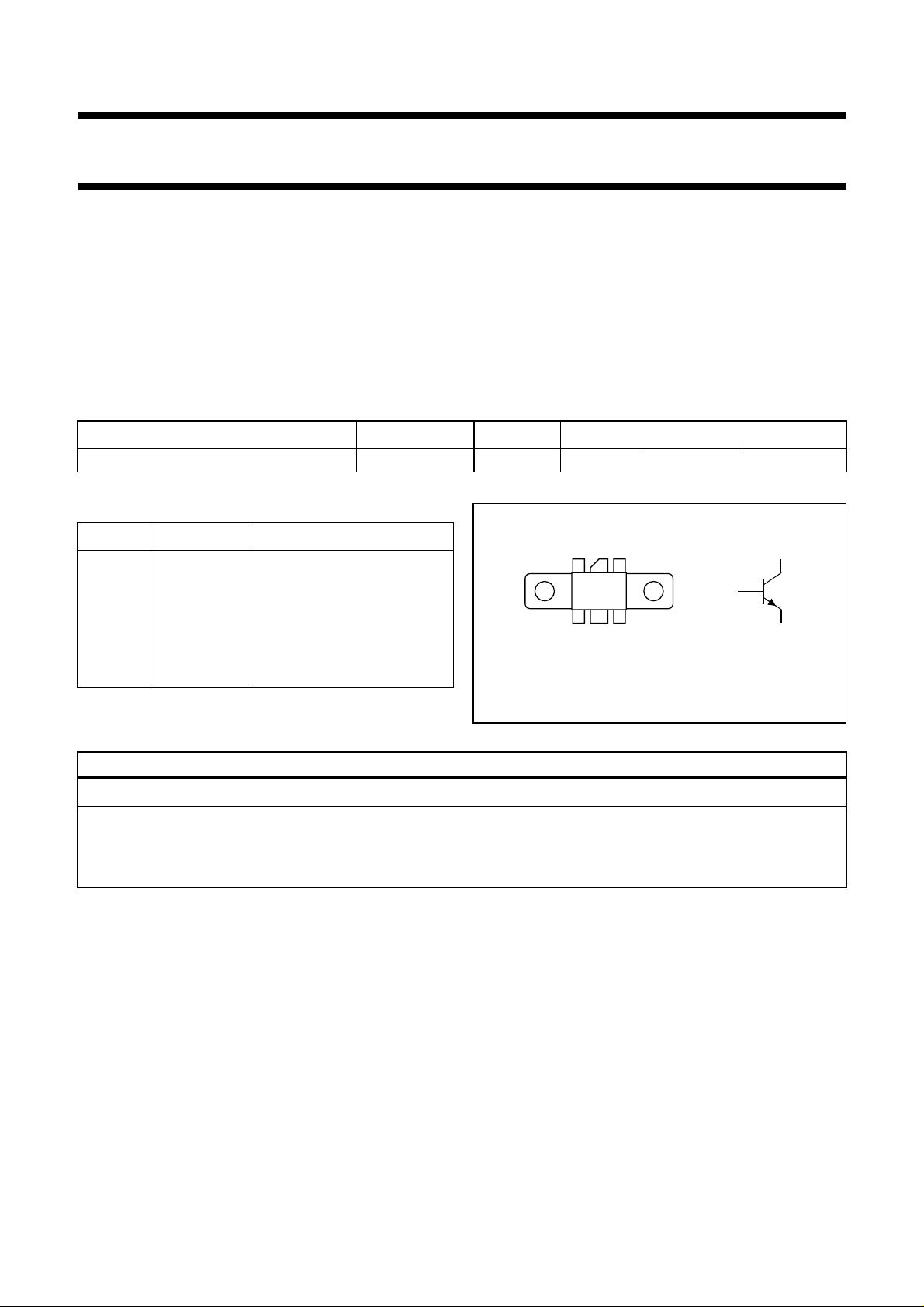
PINNING - SOT171A
PIN SYMBOL DESCRIPTION
1 e emitter
2 e emitter
3 b base
4 c collector
5 e emitter
6 e emitter
DESCRIPTION
NPN silicon planar epitaxial transistor in an SOT-171
envelope, intended for common emitter, class-AB
operation in radio transmitters for the 960 MHz
communications band. The transistor has a 6-lead flange
envelope, with a ceramic cap. All leads are isolated from
the flange.
(V) PL(W) GP(dB) ηc(%)
CE
handbook, halfpage
Top view
12345
6
b
MAM141
c
e
Fig.1 Simplified outline and symbol.
WARNING
Product and environmental safety - toxic materials
This product contains beryllium oxide. The product is entirely safe provided that the BeO disc is not damaged.
All persons who handle, use or dispose of this product should be aware of its nature and of the necessary safety
precautions. After use, dispose of as chemical or special waste according to the regulations applying at the location of
the user. It must never be thrown out with the general or domestic waste.
March 1993 2
Page 3
Philips Semiconductors Product specification
UHF power transistor BLV98CE
LIMITING VALUES
Limiting values in accordance with the Absolute Maximum System (IEC 134)
SYMBOL PARAMETER CONDITIONS MIN. MAX. UNIT
V
CBO
V
CEO
V
EBO
I
C
I
CM
P
tot
T
stg
T
j
THERMAL RESISTANCE
collector base voltage open emitter − 50 V
collector emitter voltage open base − 27 V
emitter base voltage open collector − 3.5 V
collector current DC or average − 1.5 A
collector current peak value
− 4.5 A
f > 1 MHz
total power dissipation f > 1 MHz
− 40 W
Tmb=25°C
storage temperature −65 150 °C
operating junction temperature − 200 °C
SYMBOL PARAMETER CONDITIONS TYP. MAX. UNIT
R
thj-mb
R
th mb-h
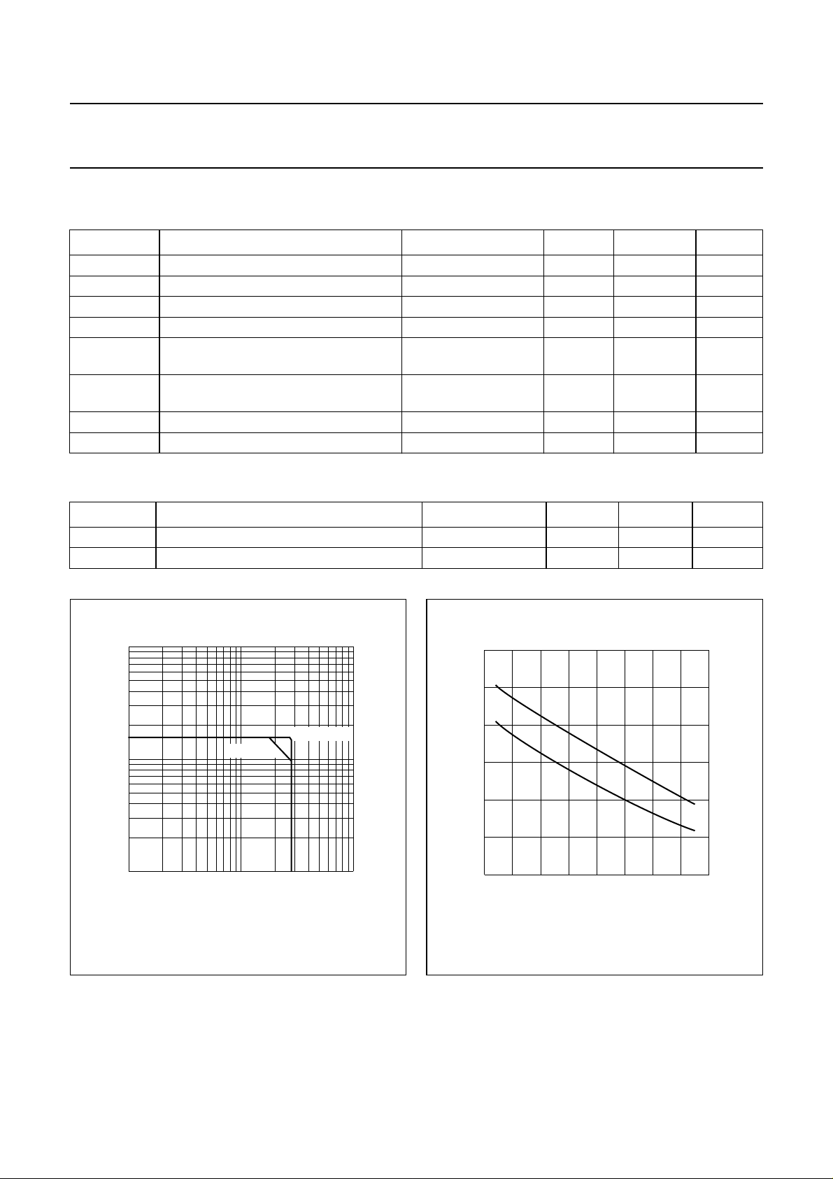
10
handbook, halfpage
I
C
(A)
1
−1
10
from junction to mounting base (RF) − 4.4 K/W
from mounting base to heatsink − 0.4 K/W
MDA449
Tmb = 25 °C
Th = 70 °C
110
V
(V)
CE
2
10
60
handbook, halfpage
P
tot
(W)
40
20
0
0
(1) DC or RF operation
(2) short-term operation during mismatch
40
(2)
(1)
80 160120
MDA450
Th (°C)
Fig.2 DC SOAR.
March 1993 3
Fig.3 Power/temperature derating.
Page 4
Philips Semiconductors Product specification
UHF power transistor BLV98CE
CHARACTERISTICS
at T
=25°C unless otherwise stated.
j
SYMBOL PARAMETER CONDITIONS MIN. TYP. MAX. UNIT
V
(BR)CBO
V
(BR)CEO
V
(BR)EBO
I
CES
h
FE
C
c
C
re
C
cf
collector-base breakdown voltage open emitter
IC= 25 mA
collector-emitter breakdown voltage open base
IC= 50 mA
emitter-base breakdown voltage open collector
IE= 5 mA
collector leakage current VBE=0
VCE= 27 V
DC current gain IC=1 A
VCE= 20 V
collector capacitance at f = 1 MHz IE=Ie=0
VCB= 24 V
feedback capacitance at f = 1 MHz IC=0
VCE= 24 V
collector-flange capacitance − 2 − pF
50 −−V
27 −−V
3.5 −−V
−− 5mA
15 −−
− 23 − pF
− 14 − pF
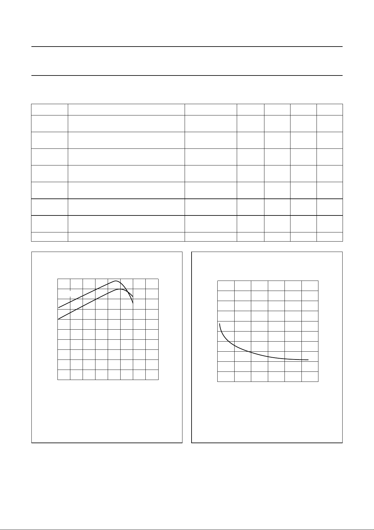
100
handbook, halfpage
h
FE
V
CE
80
60
40
20
0
012
= 24 V
20 V
MDA451
3
IC (A)
Fig.4 DC current gain as a function of collector
current; typical values.
100
handbook, halfpage
C
c
(pF)
80
60
40
20
4
0
010
20 30
MDA452
V
(V)
CB
Fig.5 Output capacitance as a function of VCB;
typical values.
March 1993 4
Page 5

Philips Semiconductors Product specification
UHF power transistor BLV98CE
APPLICATION INFORMATION
RF performance in a common emitter test circuit.
T
=25°C, R
h
= 0.4 K/W unless otherwise specified.
th mb-h
MODE OF OPERATION f (MHz) V
c.w. class-AB 960 24 30 15 > 7.5
10
handbook, halfpage
G
p
(dB)
8
6
4
2
0
025
510
G
p
η
15
20
MDA453
PL (W)
(V) I
CE
100
η
(%)
80
60
40
20
0
(mA) PL(W) GP(dB) ηc(%)
C(ZS)
typ. 8.5
30
handbook, halfpage
P
L
(W)
20
10
0
0
2
486
> 50
typ. 55
MDA454
PS (W)
Fig.6 Power gain and efficiency as a function of
load power; typical values.
March 1993 5
Fig.7 Load power as a function of input power;
typical values.
Ruggedness in class-AB operation
The BLV98CE is capable of withstanding a load mismatch
corresponding to VSWR = 50 through all phases, under
the following conditions: VCE= 24 V, I
C(ZS)
= 30 mA,
f = 960 MHz at rated output power.
Page 6

Philips Semiconductors Product specification
UHF power transistor BLV98CE
handbook, full pagewidth
50 Ω
input
R1
V
B
C7
L1 L2 L3
C1
L6
C2
C6 C8
L5
D.U.T.
C5
L4 L9
C3 C4 C12
C11 C14
L10
R2
L8
L7
L11 L12 L13
C13 C15 C16
C17
V
CC
C10C9
50 Ω
output
MDA455
Fig.8 Test circuit BLV98CE class-AB.
March 1993 6
Page 7

Philips Semiconductors Product specification
UHF power transistor BLV98CE
List of components (Fig.8)
DESIGNATION DESCRIPTION VALUE DIMENSIONS CATALOGUE NO.
C1, C6, C7,
C8,C17
C2, C3, C15,
C16
C4, C5 multilayer ceramic chip capacitor
C9 35 V solid aluminium capacitor 2.2 µF 2222 128 50228
C10 multilayer ceramic chip capacitor 3 × 100 nF
C11, C12 multilayer ceramic chip capacitor
C13, C14 multilayer ceramic chip capacitor
L1, L13 microstrip
L2, L12 microstrip
L3 microstrip
L4 microstrip
L5 3 turns enamelled 0.8 mm copper wire int. dia. 3 mm
L6, L8 grade 3B ferroxcube wide-band RF
L7 4 turns enamelled 0.8 mm copper wire int. dia. 4 mm
L9 microstrip
L10 microstrip
L11 microstrip
R1, R2 0.4 W metal film resistor 10 Ω 2322 151 71009
multilayer ceramic chip capacitor 330 pF
film dielectric trimmer 1.4 to 5.5 pF 2222 809 09001
4.3 pF
note 1
in parallel
5.6 pF
note 1
5.1 pF
note 2
50 Ω 9.0 × 2.4 mm
note 3
50 Ω 23.0 × 2.4 mm
note 3
50 Ω 16.0 × 2.4 mm
note 3
43 Ω 3.0 × 3.0 mm
note 3
length 5 mm
leads 2 × 5mm
4312 020 36642
choke
length 5 mm
leads 2 × 5mm
43 Ω 3.5 × 3.0 mm
note 3
43 Ω 11.0 × 3.0 mm
note 3
50 Ω 4.5 × 2.4 mm
note 3
Notes
1. ATC capacitor type 100A or capacitor of the same quality.
2. ATC capacitor type 100B or capacitor of the same quality.
3. The microstrips are on a double copper-clad PCB with PTFE fibre-glass dielectric (ε
March 1993 7
= 2.2); thickness1⁄32 inch.
r
Page 8

Philips Semiconductors Product specification
UHF power transistor BLV98CE
handbook, full pagewidth
122 mm
copper straps copper straps
rivetsrivets
rivets
M2
copper straps copper straps
M3
C7 L6
L8
rivets
rivetsrivets
70 mm
R1
C6
C1
L1
The circuit and components are located on one side of the PTFE fibre-glass board, the other
side being fully metallized, to serve as an earth. Earth connections are made by fixing screws,
hollow rivets and copper straps around the board and under the emitters, to provide a direct
contact between the component side and the ground plane.
L2 L3
C3C3 C16
C4
L4
L9
C5 C12 C13
Fig.9 Printed circuit board and component layout for 960 MHz test circuit.
March 1993 8
C8
C11
L10
R2
C10
L7L5
C15
C9
L12L11 L13
C17
MDA456
Page 9

Philips Semiconductors Product specification
UHF power transistor BLV98CE
Z
(Ω)
6
i
4
2
0
800
850
x
i
r
i
900 1000
950
f (MHz)
handbook, halfpage
Fig.10 Input impedance; series components;
VCE= 24 V; PL= 15 W;
R
= 0.4 K/W; typical values.
th mb-h
MDA457
Z
(Ω)
6
X
850
L
R
L
900 1000
950
f (MHz)
L
4
2
0
800
handbook, halfpage
Fig.11 Load impedance; series components;
VCE= 24 V; PL= 15 W; R
th mb-h
typical values.
MDA458
= 0.4 K/W;
950
MDA459
f (MHz)
1000
10
handbook, halfpage
G
p
(dB)
8
6
4
2
0
800 850 900
Fig.12 Power gain; class-AB operation;
VCE= 24 V; PL= 15 W; R
th mb-h
= 0.4 K/W;
typical values.
March 1993 9
Page 10

Philips Semiconductors Product specification
UHF power transistor BLV98CE
PACKAGE OUTLINE
Flanged ceramic package; 2 mounting holes; 6 leads SOT171A
D
A
F
D
1
U
1
q
H
1
b
1
2
H
U
2
Db
9.25
9.04
0.364
0.356
1
D
1
9.30
8.99
0.366
0.354
5.95
5.74
0.234
0.226
A
DIMENSIONS (millimetre dimensions are derived from the original inch dimensions)
UNIT
mm
inches
A
6.81
6.07
0.268
0.239
2.15
1.85
0.085
0.073
b
1
3.20
2.89
0.126
0.114
c
0.16
0.07
0.006
0.003
6
345
b
e
0 5 10 mm
E
E
1
6.00
5.70
0.236
0.224
e
3.58
0.140
C
w
M
C
2
p
w
M
3
scale
F
H
11.31
3.05
10.54
2.54
0.445
0.120
0.415
0.100
B
w
H
1
9.27
9.01
0.365
0.355
1
M
3.43
3.17
0.135
0.125
AB
p
c
E
1
Q
qw
18.42
U
24.90
24.63
0.980
0.970
1
6.00
5.70
0.236
0.224
Q
4.32
4.11
0.170
0.162
E
w
U
2
2
1
w
0.260.51 1.02
0.010.02 0.040.725
3
OUTLINE
VERSION
SOT171A 97-06-28
IEC JEDEC EIAJ
REFERENCES
EUROPEAN
PROJECTION
March 1993 10
ISSUE DATE
Page 11

Philips Semiconductors Product specification
UHF power transistor BLV98CE
DEFINITIONS
Data Sheet Status
Objective specification This data sheet contains target or goal specifications for product development.
Preliminary specification This data sheet contains preliminary data; supplementary data may be published later.
Product specification This data sheet contains final product specifications.
Limiting values
Limiting values given are in accordance with the Absolute Maximum Rating System (IEC 134). Stress above one or
more of the limiting values may cause permanent damage to the device. These are stress ratings only and operation
of the device at these or at any other conditions above those given in the Characteristics sections of the specification
is not implied. Exposure to limiting values for extended periods may affect device reliability.
Application information
Where application information is given, it is advisory and does not form part of the specification.
LIFE SUPPORT APPLICATIONS
These products are not designed for use in life support appliances, devices, or systems where malfunction of these
products can reasonably be expected to result in personal injury. Philips customers using or selling these products for
use in such applications do so at their own risk and agree to fully indemnify Philips for any damages resulting from such
improper use or sale.
March 1993 11
 Loading...